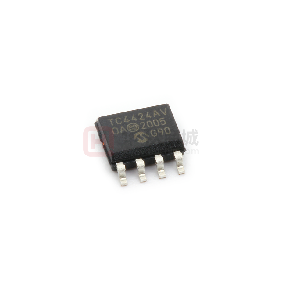
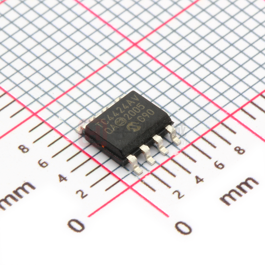
0
登录后你可以
  • 下载海量资料
  • 学习在线课程
  • 观看技术视频
  • 写文章/发帖/加入社区
创作中心
发布
  • 发文章

  • 发资料

  • 发帖

  • 提问

  • 发视频

创作活动
TC4424AVOA713

TC4424AVOA713

  • 厂商:

    ACTEL(微芯科技)

  • 封装:

    SOIC8_150MIL

  • 描述:

    3A双高速功率MOSFET驱动器

  • 数据手册
  • 价格&库存
TC4424AVOA713 数据手册
TC4423A/TC4424A/TC4425A 3A Dual High-Speed Power MOSFET Drivers Features General Description • High Peak Output Current: 4.5A (typical) • Wide Input Supply Voltage Operating Range: - 4.5V to 18V • High Capacitive Load Drive Capability: - 1800 pF in 12 ns • Short Delay Times: 40 ns (typical) • Matched Rise/Fall Times • Low Supply Current: - With Logic ‘1’ Input – 1.0 mA (maximum) - With Logic ‘0’ Input – 150 µA (maximum) • Low Output Impedance: 2.5Ω (typical) • Latch-Up Protected: Will Withstand 1.5A Reverse Current • Logic Input Will Withstand Negative Swing Up To 5V • Pin compatible with the TC4423/TC4424/TC4425 and TC4426A/TC4427A/TC4428A devices • Space-saving 8-Pin 150 mil body SOIC and 8-Pin 6x5 DFN Packages The TC4423A/TC4424A/TC4425A devices are a family of dual-output 3A buffers/MOSFET drivers. These devices are improved versions of the earlier TC4423/ TC4424/TC4425 dual-output 3A driver family. This improved version features higher peak output current drive capability, lower shoot-throught current, matched rise/fall times and propagation delay times. The TC4423A/TC4424A/TC4425A devices are pincompatible with the existing TC4423/TC4424/TC4425 family. An 8-pin SOIC package option has been added to the family. The 8-pin DFN package option offers increased power dissipation capability for driving heavier capacitive or resistive loads. The TC4423A/TC4424A/TC4425A MOSFET drivers can easily charge and discharge 1800 pF gate capacitance in under 20 ns, provide low enough impedances in both the on and off states to ensure the MOSFET’s intended state will not be affected, even by large transients. The TC4423A/TC4424A/TC4425A inputs may be driven directly from either TTL or CMOS (2.4V to 18V). In addition, the 300 mV of built-in hysteresis provides noise immunity and allows the device to be driven from slow rising or falling waveforms. Applications • • • • Switch Mode Power Supplies Pulse Transformer Drive Line Drivers Direct Drive of Small DC Motors The TC4423A/TC4424A/TC4425A dual-output 3A MOSFET driver family is offerd with a -40oC to +125oC temperature rating, making it useful in any wide temperature range application. Package Types 8-Pin PDIP/SOIC TC4423A TC4424A TC4425A NC IN A GND IN B 8 1 2 TC4423A 7 3 TC4424A 6 4 TC4425A 5 8-Pin 6x5 DFN (1) NC 1 IN A 2 GND 3 IN B 4 NC OUT A VDD OUT B TC4423A TC4424A TC4425A NC OUT A VDD OUT B NC OUT A VDD OUT B TC4423A TC4424A TC4425A 8 NC NC NC 7 OUT A OUT A OUT A 6 VDD VDD VDD 5 OUT B OUT B OUT B TC4423A TC4424A TC4425A 16-Pin SOIC (Wide) NC IN A NC GND GND NC IN B NC 1 16 2 15 3 4 5 6 7 8 TC4423A TC4424A TC4425A 14 13 12 11 10 9 NC OUT A OUT A VDD VDD OUT B OUT B NC NC OUT A OUT A VDD VDD OUT B OUT B NC NC OUT A OUT A VDD VDD OUT B OUT B NC Note 1: Exposed pad of the DFN package is electrically isolated. 2: Duplicate pins must both be connected for proper operation. © 2007 Microchip Technology Inc. DS21998B-page 1 TC4423A/TC4424A/TC4425A Functional Block Diagram(1) Inverting VDD 750 µA 300 mV Output Non-inverting Input Effective Input C = 20 pF (Each Input) GND 4.7V TC4423A Dual Inverting TC4424A Dual Non-inverting TC4425A Inverting / Non-inverting Note 1: Unused inputs should be grounded. DS21998B-page 2 © 2007 Microchip Technology Inc. TC4423A/TC4424A/TC4425A 1.0 ELECTRICAL CHARACTERISTICS † Notice: Stresses above those listed under "Maximum Ratings" may cause permanent damage to the device. This is a stress rating only and functional operation of the device at those or any other conditions above those indicated in the operational sections of this specification is not intended. Exposure to maximum rating conditions for extended periods may affect device reliability. Absolute Maximum Ratings † Supply Voltage ................................................................+20V Input Voltage, IN A or IN B .......... (VDD + 0.3V) to (GND – 5V) Package Power Dissipation (TA=50°C) 8L PDIP .......................................................................1.2W 8L SOIC.................................................................... 0.61W 16L SOIC.....................................................................1.1W 8L DFN .................................................................... Note 3 DC CHARACTERISTICS (NOTE 2) Electrical Specifications: Unless otherwise indicated, TA = +25°C, with 4.5V ≤ VDD ≤ 18V. Parameters Sym Min Typ Max Units Logic ‘1’, High Input Voltage VIH 2.4 1.5 — V Logic ‘0’, Low Input Voltage VIL — 1.3 0.8 V Input Current IIN –1 — 1 µA Input Voltage VIN -5 — VDD+0.3 V Conditions Input 0V ≤ VIN ≤ VDD Output High Output Voltage VOH VDD – 0.025 — — V DC Test Low Output Voltage VOL — — 0.025 V DC Test Output Resistance, High ROH — 2.2 3.0 Ω IOUT = 10 mA, VDD = 18V Output Resistance, Low ROL — 2.8 3.5 Ω IOUT = 10 mA, VDD = 18V Peak Output Current IPK — 4.5 — A 10V≤ VDD ≤18V (Note 2) Latch-Up Protection Withstand Reverse Current IREV — >1.5 — A Duty cycle ≤ 2%, t ≤ 300 µsec. Rise Time tR — 12 21 ns Figure 4-1, Figure 4-2, CL = 1800 pF Fall Time tF — 12 21 ns Figure 4-1, Figure 4-2, CL = 1800 pF Delay Time tD1 — 40 48 ns Figure 4-1, Figure 4-2, CL = 1800 pF Delay Time tD2 — 41 48 ns Figure 4-1, Figure 4-2, CL = 1800 pF VDD 4.5 — 18 V IS — 1.0 2.0 mA VIN = 3V (Both inputs) IS — 0.15 0.25 mA VIN = 0V (Both inputs) Switching Time (Note 1) Power Supply Supply Voltage Power Supply Current Note 1: 2: 3: Switching times ensured by design. Tested during characterization, not production tested. Package power dissipation is dependent on the copper pad area on the PCB. © 2007 Microchip Technology Inc. DS21998B-page 3 TC4423A/TC4424A/TC4425A DC CHARACTERISTICS (OVER OPERATING TEMPERATURE RANGE) Electrical Specifications: Unless otherwise indicated, operating temperature range with 4.5V ≤ VDD ≤ 18V. Parameters Sym Min Typ Max Units Logic ‘1’, High Input Voltage VIH 2.4 Logic ‘0’, Low Input Voltage VIL — Input Current IIN High Output Voltage Low Output Voltage Conditions — — V — 0.8 V –10 — +10 µA VOH VDD – 0.025 — — V VOL — — 0.025 V Output Resistance, High ROH — 3.1 6 Ω IOUT = 10 mA, VDD = 18V Output Resistance, Low ROL — 3.7 7 Ω IOUT = 10 mA, VDD = 18V Rise Time tR — 20 31 ns Figure 4-1, Figure 4-2, CL = 1800 pF Fall Time tF — 22 31 ns Figure 4-1, Figure 4-2, CL = 1800 pF Delay Time tD1 — 50 66 ns Figure 4-1, Figure 4-2, CL = 1800 pF Delay Time tD2 — 50 66 ns Figure 4-1, Figure 4-2, CL = 1800 pF IS — — 2.0 0.2 3.0 0.3 mA VIN = 3V (Both inputs) VIN = 0V (Both inputs) Input 0V ≤ VIN ≤ VDD Output Switching Time (Note 1) Power Supply Power Supply Current Note 1: Switching times ensured by design. TEMPERATURE CHARACTERISTICS Electrical Specifications: Unless otherwise noted, all parameters apply with 4.5V ≤ VDD ≤ 18V. Parameters Sym Min Typ Max Units Conditions Temperature Ranges Specified Temperature Range (V) TA –40 — +125 °C Maximum Junction Temperature TJ — — +150 °C Storage Temperature Range TA –65 — +150 °C Thermal Resistance, 8L-6x5 DFN θJA — 33.2 — °C/W Thermal Resistance, 8L-PDIP θJA — 84.6 — °C/W Thermal Resistance, 8L-SOIC θJA — 163 — °C/W Thermal Resistance, 16L-SOIC θJA — 90 — °C/W Package Thermal Resistances DS21998B-page 4 Typical four-layer board with vias to ground plane © 2007 Microchip Technology Inc. TC4423A/TC4424A/TC4425A 2.0 TYPICAL PERFORMANCE CURVES Note: The graphs and tables provided following this note are a statistical summary based on a limited number of samples and are provided for informational purposes only. The performance characteristics listed herein are not tested or guaranteed. In some graphs or tables, the data presented may be outside the specified operating range (e.g., outside specified power supply range) and therefore outside the warranted range. Note: Unless otherwise indicated, TA = +25°C with 4.5V
TC4424AVOA713 价格&库存

很抱歉,暂时无法提供与“TC4424AVOA713”相匹配的价格&库存,您可以联系我们找货

免费人工找货
TC4424AVOA713
  •  国内价格
  • 1+4.36151
  • 10+4.20901
  • 100+3.84301
  • 500+3.66001

库存:1836