TC7650
Chopper Stabilized Operational Amplifier
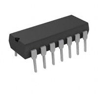
Package Type
Features
•
•
•
•
•
•
•
•
•
•
Low Input Offset Voltage: 0.7µV Typ
Low Input Offset Voltage Drift: 0.05V/°C Max
Low Input Bias Current: 10pA Max
High Impedance Differential CMOS Inputs: 1012
High Open Loop Voltage Gain: 120dB Min.
Low Input Noise Voltage: 2.0Vp-p
High Slew Rate: 2.5V/sec.
Low Power Operation: 20mW
Output Clamp Speeds Recovery Time
Compensated Internally for Stable Unity Gain
Operation
• Direct Replacement for ICL7650
• Available in 8-Pin Plastic DIP and 14-Pin Plastic
DIP Packages
Applications
•
•
•
•
•
Instrumentation
Medical Instrumentation
Embedded Control
Temperature Sensor Amplifier
Strain Gage Amplifier
Part
Number
Package
TC7650CPA
8-Pin PDIP
0°C to +70°C
5V
TC7650CPD 14-Pin PDIP
0°C to +70°C
5V
2001-2012 Microchip Technology Inc.
8 CB
CA 1
7 VDD
– INPUT 2
+ INPUT 3
VSS
TC7650CPA 6 OUTPUT
5 OUTPUT CLAMP
4
14-Pin DIP
CB
1
14 INT/EXT
CA
2
13 EXT CLK IN
NC
3
12 INT CLK OUT
– INPUT
4
+ INPUT
5
10 OUTPUT
NC
6
9 OUTPUT CLAMP
VSS
7
8 CRETN
TC7650CPD 11 VDD
NC = NO INTERNAL CONNECTION
Device Selection Table
Temperature
Range
8-Pin DIP
Max VOS
DS21463C-page 1
�TC7650
General Description
The TC7650 CMOS chopper stabilized operational
amplifier practically removes offset voltage error terms
from system error calculations. The 5V maximum VOS
specification, for example, represents a 15 times
improvement over the industry standard OP07E. The
50nV/°C offset drift specification is over 25 times lower
than the OP07E. The increased performance eliminates VOS trim procedures, periodic potentiometer
adjustment and the reliability problems caused by damaged trimmers.
The TC7650 performance advantages are achieved
without the additional manufacturing complexity and
cost incurred with laser or "zener zap" VOS trim techniques.
The TC7650 nulling scheme corrects both DC VOS
errors and VOS drift errors with temperature. A nulling
amplifier alternately corrects its own VOS errors and the
main amplifier VOS error. Offset nulling voltages are
stored on two user supplied external capacitors. The
capacitors connect to the internal amplifier VOS null
points. The main amplifier input signal is never
switched. Switching spikes are not present at the
TC7650 output.
The 14-pin dual-in-line package (DIP) has an external
oscillator input to drive the nulling circuitry for optimum
noise performance. Both the 8 and 14-pin DIPs have
an output voltage clamp circuit to minimize overload
recovery time.
Functional Block Diagram
Output
Clamp
14-Pin DIP Only
Output Clamp
Circuit
INT/EXT
EXT CLK IN
CLK OUT
Oscillator
Main
Amplifier
A
Inputs
B
Output
CB
NULL
Intermod
Compensation
B
B
B
A
CA
Null
Amplifier
TC7650
A
Null
*CRETN
* For 8-Pin DIP, connect to Vss
DS21463C-page 2
2001-2012 Microchip Technology Inc.
�TC7650
1.0
ELECTRICAL
CHARACTERISTICS
ABSOLUTE MAXIMUM RATINGS*
Total Supply Voltage (VDD to VSS) ....................... +18V
Input Voltage .................... (VDD +0.3V) to (VSS – 0.3V)
Storage Temperature Range.............. -65°C to +150°C
Voltage on Oscillator Control Pins...............VDD to VSS
Duration of Output Short Circuit .....................Indefinite
Current Into Any Pin............................................ 10mA
While Operating (Note 3)............................100µA
Package Power Dissipation (TA 70°C)
8-Pin Plastic DIP ....................................... 730mW
14-Pin Plastic DIP ..................................... 800mW
Operating Temperature Range
C Device .......................................... 0°C to +70°C
*Stresses above those listed under “Absolute Maximum
Ratings” may cause permanent damage to the device.
These are stress ratings only and functional operation of the
device at these or any other conditions above those indicated in the operation sections of the specifications is not
implied. Exposure to Absolute Maximum Rating conditions
for extended periods my affect device reliability.
TC7652 ELECTRICAL SPECIFICATIONS
Electrical Characteristics: VDD = +5V, VSS = -5V, CA = CB = 0.1F, TA = +25°C, unless otherwise indicated.
Symbol
Parameter
Min.
Typ
Max
Units
Test Conditions
Input
VOS
Input Offset Voltage
—
—
±0.7
±1.0
±5
—
—
V
VOS/T
Input Offset Voltage Average
Temperature Coefficient
—
0.01
0.05
V/°C
Offset Voltage vs. Time
—
100
—
nV/
month
IBIAS
Input Bias Current
—
—
—
1.5
35
100
10
150
400
pA
pA
pA
IOS
Input Offset Current
—
0.5
—
pA
eNP-P
Input Noise Voltage
—
2
—
VP-P
IN
Input Noise Current
—
0.01
—
pA/Hz
RIN
Input Resistance
—
1012
TA = +25°C
Over Operating Temp Range
Operating Temperature Range
TA = +25°C
0°C TA +70°C
-25°C TA +85°C
RS = 100, 0 to 10Hz
f = 10Hz
CMVR
Common Mode Voltage Range
-5
-5.2 to +2
+1.6
V
CMRR
Common Mode Rejection Ratio
120
130
—
dB
CMVR = -5V to +1.5V
RL = 10k
Output
A
Large Signal Voltage Gain
120
130
—
dB
VOUT
Output Voltage Swing (Note 2)
±4.7
—
±4.85
±4.95
—
—
V
V
Clamp ON Current
25
70
200
A
RL = 100k (Note 1)
Clamp OFF Current
—
1
—
pA
-4V < VOUT < +4V (Note 1)
RL = 10k
RL = 100k
Dynamic
BW
Unity Gain Bandwidth
—
2.0
—
MHz
SR
Slew Rate
—
2.5
—
V/sec
tR
Rise Time
—
0.2
—
sec
Overshoot
Unity Gain (+1)
CL = 50pF, RL = 10k
—
20
—
%
Internal Chopping Frequency
120
200
375
Hz
VDD, VSS
Operating Supply Range
4.5
—
16
V
IS
Supply Current
—
2
3.5
mA
No Load
PSRR
Power Supply Rejection Ratio
120
130
dB
VS = ±3V to ±8V
fCH
Pins 12–14 Open (DIP)
Supply
Note
1:
2:
3:
See "Output Clamp" discussion.
Output clamp not connected. See typical characteristics curves for output swing versus clamp current characteristics.
Limiting input current to 100A is recommended to avoid latch-up problems.
2001-2012 Microchip Technology Inc.
DS21463C-page 3
�TC7650
2.0
PIN DESCRIPTIONS
The descriptions of the pins are listed in Table 2-1.
TABLE 2-1:
PIN FUNCTION TABLE
Pin Number
Symbol
Description
8-pin DIP
14-pin DIP
1,8
2,1
CA, CB
Nulling capacitor pins
2
4
-INPUT
Inverting Input
3
5
+INPUT
4
7
VSS
5
9
OUTPUT
CLAMP
Output Voltage Clamp
6
10
OUTPUT
Output
7
11
VDD
Positive Power Supply
—
3,6
NC
No internal connection
—
8
—
12
CRETN
—
13
EXT CLK IN
—
14
INT/EXT
Non-inverting Input
Negative Power Supply
Capacitor current return pin
INT CLK OUT Internal Clock Output
External Clock Input
Select Internal or External Clock
3.0
DETAILED DESCRIPTION
After the nulling amplifier is zeroed, the main amplifier
is zeroed; the A switches open and B switches close.
3.1
Theory of Operation
The output voltage equation is:
Figure 3-1 shows the major elements of the TC7650.
There are two amplifiers (the main amplifier and the
nulling amplifier), and both have offset null capability.
The main amplifier is connected full-time from the input
to the output. The nulling amplifier, under the control of
the chopping frequency oscillator and clock circuit,
alternately nulls itself and the main amplifier. Two external capacitors provide the required storage of the nulling potentials and the necessary nulling loop time
constants. The nulling arrangement operates over the
full common mode and power supply ranges, and is
also independent of the output level, thus giving exceptionally high CMRR, PSRR and AVOL.
Careful balancing of the input switches minimizes
chopper frequency charge injection at the input terminals, and the feed forward type injection into the compensation capacitor that can cause output spikes in this
type of circuit.
The circuit's offset voltage compensation is easily
shown. With the nulling inputs shorted, a voltage
almost identical to the nulling amplifier offset voltage is
stored on CA. The effective offset voltage at the null
amplifier input is:
EQUATION 3-1:
1
V OSE = ------------------ V OSN
A +1
N
DS21463C-page 4
EQUATION 3-2:
VOUT = AMVOSM + (V+ - V-) + AN(V+ - V-) + AN VOSE
EQUATION 3-3:
V OSM + V OSN
+
V OUT = A M A N V – V + ------------------------------------------AN
As desired, the device offset voltages are reduced by
the high open loop gain of the nulling amplifier.
3.2
Output Stage/Loading
The output circuit is a high impedance stage (approximately 18k). With loads less than this, the chopper
amplifier behaves in some ways like a trans-conductance amplifier whose open-loop gain is proportional to
load resistance. For example, the open loop gain will
be 17dB lower with a 1k load than with a 10k load.
If the amplifier is used strictly for DC, the lower gain is
of little consequence, since the DC gain is typically
greater than 120dB, even with a 1k load. In wideband
applications, the best frequency response will be
achieved with a load resistor of 10k or higher. This
results in a smooth 6dB/octave response from 0.1Hz to
2MHz, with phase shifts of less than 10° in the transi-
2001-2012 Microchip Technology Inc.
�TC7650
tion region, where the main amplifier takes over from
the null amplifier. The clock frequency sets the transition region.
3.3
Intermodulation
Previous chopper stabilized amplifiers have suffered
from intermodulation effects between the chopper frequency and input signals. These arise because the
finite AC gain of the amplifier results in a small AC signal at the input. This is seen by the zeroing circuit as an
error signal, which is chopped and fed back, thus injectFIGURE 3-1:
ing sum and difference frequencies, and causing disturbances to the gain and phase versus frequency
characteristics near the chopping frequency. These
effects are substantially reduced in the TC7650 by
feeding the nulling circuit with a dynamic current corresponding to the compensation capacitor current in such
a way as to cancel that portion of the input signal due
to a finite AC gain. The intermodulation and gain/phase
disturbances are held to very low values, and can generally be ignored.
TC7650 CONTAINS A NULLING AND MAIN AMPLIFIER. OFFSET CORRECTION
VOLTAGES ARE STORED ON TWO EXTERNAL CAPACITORS.
V+
Main
+ Amplifier
Null
Gain = AM
Analog Input
V-
B
VOUT
TC7650
+
A
CB
B
Null
Null
Amplifier
A
CA
Gain = AN , Offset = VOSN
FIGURE 3-2:
VDD VSS
4
11
2
-
7
10
1
+
7
-
4
+
8
8
2
CB
VSS
1
CA
CB
14-PIN PACKAGE
3.4
6
TC7650
3
CA
8-PIN PACKAGE
Nulling Capacitor Connection
The offset voltage correction capacitors are connected
to CA and CB. The common capacitor connection is
made to VSS (Pin 4) on the 8-pin packages and to
capacitor return (CRETN, Pin 8) on the 14-pin packages.
The common connection should be made through a
separate PC trace or wire to avoid voltage drops. The
capacitors outside foil, if possible, should be connected
to CRETN or VSS.
2001-2012 Microchip Technology Inc.
Clock Operation
The internal oscillator is set for a 200Hz nominal chopping frequency on both the 8- and 14-pin DIPs. With the
14-pin DIP TC7650, the 200 Hz internal chopping frequency is available at the internal clock output (Pin 12).
A 400Hz nominal signal will be present at the external
clock input pin (Pin 13) with INT/EXT high or open. This
is the internal clock signal before a divide-by-two operation.
VDD
TC7650
5
3.5
NULLING CAPACITOR
CONNECTION
The 14-pin DIP device can be driven by an external
clock. The INT/EXT input (Pin 14) has an internal pullup and may be left open for internal clock operation. If
an external clock is used, INT/EXT must be tied to VSS
(Pin 7) to disable the internal clock. The external clock
signal is applied to the external clock input (Pin 13).
The external clock amplitude should swing between
VDD and ground for power supplies up to ±6V and
between V+ and V+ -6V for higher supply voltages.
At low frequencies the external clock duty cycle is not
critical, since an internal divide-by-two gives the
desired 50% switching duty cycle. The offset storage
correction capacitors are charged only when the external clock input is high. A 50% to 80% external clock
DS21463C-page 5
�TC7650
positive duty cycle is desired for frequencies above
500Hz to ensure transients settle before the internal
switches open.
The external clock input can also be used as a strobe
input. If a strobe signal is connected at the external
clock input so that it is LOW during the time an overload
signal is applied, neither capacitor will be charged. The
leakage currents at the capacitors pins are very low. At
25°C a typical TC7650 will drift less than 10V/sec.
3.6
FIGURE 3-5:
INVERTING AMPLIFIER WITH
OPTIONAL CLAMP
R2
Clamp
R1
Input
TC7650 C
+
C
Output Clamp
Chopper-stabilized systems can show long recovery
times from overloads. If the output is driven to either
supply rail, output saturation occurs. The inputs are no
longer held at a "virtual ground." The VOS null circuit
treats the differential signal as an offset and tries to correct it by charging the external capacitors. The nulling
circuit also saturates. Once the input signal returns to
normal, the response time is lengthened by the long
recovery time of the nulling amplifier and external
capacitors.
Through an external clamp connection, the TC7650
eliminates the overload recovery problem by reducing
the feedback network gain before the output voltage
reaches either supply rail.
FIGURE 3-3:
INTERNAL CLAMP CIRCUIT
Internal
Positive Clamp Bias ≈ V+ - VT ≈ V+ - 0.7
P-Channel
Output
Clamp Pin
N-Channel
FIGURE 3-4:
NON-INVERTING AMPLIFIER
WITH OPTIONAL CLAMP
0.1µF
* Connect To VSS
On 8-Pin DIP.
Input
C
+
*
R
Output
TC7650 C
R2
Clamp
R3
R3 + (R1/R2) ‡ 100 kΩ
For Full Clamp Effect
DS21463C-page 6
R1
–
* Connect To VR
On 8-Pin DIP.
Output
R *
(R1 R2) ‡ 100 kΩ
For Full Clamp
Effect
0.1 µ F 0.1 µ F
The output clamp circuit is shown in Figure 3-3, with
typical inverting and non-inverting circuit connections
shown in Figures 3-4 and 3-5. Output voltage versus
clamp circuit current characteristics are shown in the
typical operating curves. For the clamp to be fully effective, the impedance across the clamp output should be
greater than 100k.
3.7
Latch-Up Avoidance
Junction-isolated CMOS circuits inherently include a
parasitic 4-layer (p-n-p-n) structure which has characteristics similar to an SCR. Under certain circumstances this junction may be triggered into a lowimpedance state, resulting in excessive supply current.
To avoid this condition, no voltage greater than 0.3V
beyond the supply rails should be applied to any pin. In
general, the amplifier supplies must be established
either at the same time or before any input signals are
applied. If this is not possible, the drive circuits must
limit input current flow to under 0.1mA to avoid latchup.
3.8
Thermoelectric Potentials
Precision DC measurements are ultimately limited by
thermoelectric potentials developed in thermocouple
junctions of dissimilar metals, alloys, silicon, etc.
Unless all junctions are at the same temperature, thermoelectric voltages, typically around 0.1V/°C, but up
to tens of V/°C for some materials, will be generated.
In order to realize the benefits extremely-low offset voltages provide, it is essential to take special precautions
to avoid temperature gradients. All components should
be enclosed to eliminate air movement, especially
those caused by power dissipating elements in the system. Low thermoelectric co-efficient connections
should be used where possible and power supply voltages and power dissipation should be kept to a minimum. High impedance loads are preferable, and
separation from surrounding heat dissipating elements
is advised.
2001-2012 Microchip Technology Inc.
�TC7650
3.9
Pin Compatibility
On the 8-pin mini-DIP TC7650, the external null storage capacitors are connected to pins 1 and 8. On most
other operational amplifiers these are left open or are
used for offset potentiometer or compensation capacitor connections.
FIGURE 3-6:
INPUT GUARD CONNECTION
Inverting Amplifier
R2
R1
Input
-
For OP05 and OP07 operational amplifiers, the
replacement of the offset null potentiometer between
pins 1 and 8 by two capacitors from the pins to VSS will
convert the OP05/07 pin configurations for TC7650
operation. For LM108 devices, the compensation
capacitor is replaced by the external nulling capacitors.
The LM101/748/709 pinouts are modified similarly by
removing any circuit connections to Pin 5. On the
TC7650, Pin 5 is the output clamp connection.
R3*
Noninverting Amplifier
R2
Other operational amplifiers may use this pin as an offset or compensation point.
The minor modifications needed to retrofit a TC7650
into existing sockets operating at reduced power supply voltages make prototyping and circuit verification
straightforward.
3.10
Output
+
R3*
+
Output
R1
Input Guarding
High impedance, low leakage CMOS inputs allow the
TC7650 to make measurements of high-impedance
sources. Stray leakage paths can increase input currents and decrease input resistance unless inputs are
guarded. A guard is a conductive PC trace surrounding
the input terminals. The ring connects to a low impedance point at the same potential as the inputs. Stray
leakages are absorbed by the low impedance ring. The
equal potential between ring and inputs prevents input
leakage currents. Typical guard connections are shown
in Figure 3-6.
The 14-pin DIP configuration has been specifically
designed to ease input guarding. The pins adjacent to
the inputs are unused.
Input
NOTE: R3 =
Should Be Low
Impedence For
Optimum Guarding
R1 R2
R1 + R2
Follower
R3*
-
Input
+
Output
In applications requiring low leakage currents, boards
should be cleaned thoroughly and blown dry after soldering. Protective coatings will prevent future board
contamination.
3.11
Component Selection
The two required capacitors, CA and CB, have optimum
values, depending on the clock or chopping frequency.
For the preset internal clock, the correct value is 0.1F.
To maintain the same relationship between the chopping frequency and the nulling time constant, the
capacitor values should be scaled in proportion to the
external clock, if used. High quality film type capacitors
(such as Mylar) are preferred; ceramic or other lower
grade capacitors may be suitable in some applications.
For fast settling on initial turn-on, low dielectric absorption capacitors (such as polypropylene) should be
used. With ceramic capacitors, several seconds may
be required to settle to 1V.
2001-2012 Microchip Technology Inc.
DS21463C-page 7
�TC7650
TYPICAL CHARACTERISTICS
Note:
The graphs and tables provided following this note are a statistical summary based on a limited number of
samples and are provided for informational purposes only. The performance characteristics listed herein
are not tested or guaranteed. In some graphs or tables, the data presented may be outside the specified
operating range (e.g., outside specified power supply range) and therefore outside the warranted range.
Positive Clamp Current
vs. Output Voltage
Negative Clamp Current
vs. Output Voltage
1 mA
1 mA
0.1 mA
0.01 mA
0.01 mA
1m A
1m A
CLAMP CURRENT
CLAMP CURRENT
0.1 mA TA = +25˚C
VS = ±5V
0.1m A
0.01m A
1 nA
0.1 nA
0.01 nA
TA = +25˚C
VS = ±5V
0.1m A
0.01m A
1 nA
0.1 nA
0.01 nA
1 pA
4.0 4.1 4.2 4.3 4.4 4.5 4.6 4.7 4.8 4.9 5.0
OUTPUT VOLTAGE (V)
1 pA
-4.0 -4.1 -4.2 -4.3 -4.4 -4.5 -4.6 -4.7 -4.8 -4.9 -5.0
OUTPUT VOLTAGE (V)
Supply Current vs.
Supply Voltage
Gain/Phase vs. Frequency
3.0
2.6
30
225
20
180
135
10
GAIN
0
GAIN (dB)
SUPPLY CURRENT (mA)
TA = +25˚C
2.2
1.8
1.4
45
–10
–20
PHASE
-45
–40
-90
CLOSED-LOOP
GAIN = 20
–60
5
DS21463C-page 8
6
7
8 9 10 11 12 13 14 15
SUPPLY VOLTAGE (V)
0
–30
–50
1.0
90
1k
10k
100k
1M
FREQUENCY (Hz )
PHASE (deg)
4.0
-135
-180
10M
2001-2012 Microchip Technology Inc.
�TC7650
5.0
PACKAGING INFORMATION
5.1
Package Marking Information
Package marking information not available at this time.
5.2
Package Dimensions
Note:
For the most current package drawings, please see the Microchip Packaging Specification located
at http://www.microchip.com/packaging
8-Pin Plastic DIP
PIN 1
.260 (6.60)
.240 (6.10)
.045 (1.14)
.030 (0.76)
.070 (1.78)
.040 (1.02)
.310 (7.87)
.290 (7.37)
.400 (10.16)
.348 (8.84)
.200 (5.08)
.140 (3.56)
.040 (1.02)
.020 (0.51)
.150 (3.81)
.115 (2.92)
.110 (2.79)
.090 (2.29)
.015 (0.38)
.008 (0.20)
3˚MIN.
.400 (10.16)
.310 (7.87)
.022 (0.56)
.015 (0.38)
Dimensions: inches (mm)
Note:
For the most current package drawings, please see the Microchip Packaging Specification located
at http://www.microchip.com/packaging
14-Pin PDIP (Narrow)
PIN 1
.260 (6.60)
.240 (6.10)
.310 (7.87)
.290 (7.37)
.770 (19.56)
.745 (18.92)
.200 (5.08)
.140 (3.56)
.040 (1.02)
.020 (0.51)
.150 (3.81)
.115 (2.92)
.015 (0.38)
.008 (0.20)
3˚MIN.
.400 (10.16)
.310 (7.87)
.110 (2.79)
.090 (2.29)
.070 (1.78)
.045 (1.14)
.022 (0.56)
.015 (0.38)
Dimensions: inches (mm)
2001-2012 Microchip Technology Inc.
DS21463C-page 9
�TC7650
6.0
REVISION HISTORY
Revision C (December 2012)
Added a note to each package outline drawing.
DS21463C-page 10
2001-2012 Microchip Technology Inc.
�TC7650
SALES AND SUPPORT
Data Sheets
Products supported by a preliminary Data Sheet may have an errata sheet describing minor operational differences
and recommended workarounds. To determine if an errata sheet exists for a particular device, please contact one of
the following:
1.
2.
Your local Microchip sales office
The Microchip Worldwide Site (www.microchip.com)
Please specify which device, revision of silicon and Data Sheet (include Literature #) you are using.
New Customer Notification System
Register on our web site (www.microchip.com/cn) to receive the most current information on our products.
2001-2012 Microchip Technology Inc.
DS21463C-page 11
�TC7650
NOTES:
DS21463C-page 12
2001-2012 Microchip Technology Inc.
�Note the following details of the code protection feature on Microchip devices:
•
Microchip products meet the specification contained in their particular Microchip Data Sheet.
•
Microchip believes that its family of products is one of the most secure families of its kind on the market today, when used in the
intended manner and under normal conditions.
•
There are dishonest and possibly illegal methods used to breach the code protection feature. All of these methods, to our
knowledge, require using the Microchip products in a manner outside the operating specifications contained in Microchip’s Data
Sheets. Most likely, the person doing so is engaged in theft of intellectual property.
•
Microchip is willing to work with the customer who is concerned about the integrity of their code.
•
Neither Microchip nor any other semiconductor manufacturer can guarantee the security of their code. Code protection does not
mean that we are guaranteeing the product as “unbreakable.”
Code protection is constantly evolving. We at Microchip are committed to continuously improving the code protection features of our
products. Attempts to break Microchip’s code protection feature may be a violation of the Digital Millennium Copyright Act. If such acts
allow unauthorized access to your software or other copyrighted work, you may have a right to sue for relief under that Act.
Information contained in this publication regarding device
applications and the like is provided only for your convenience
and may be superseded by updates. It is your responsibility to
ensure that your application meets with your specifications.
MICROCHIP MAKES NO REPRESENTATIONS OR
WARRANTIES OF ANY KIND WHETHER EXPRESS OR
IMPLIED, WRITTEN OR ORAL, STATUTORY OR
OTHERWISE, RELATED TO THE INFORMATION,
INCLUDING BUT NOT LIMITED TO ITS CONDITION,
QUALITY, PERFORMANCE, MERCHANTABILITY OR
FITNESS FOR PURPOSE. Microchip disclaims all liability
arising from this information and its use. Use of Microchip
devices in life support and/or safety applications is entirely at
the buyer’s risk, and the buyer agrees to defend, indemnify and
hold harmless Microchip from any and all damages, claims,
suits, or expenses resulting from such use. No licenses are
conveyed, implicitly or otherwise, under any Microchip
intellectual property rights.
Trademarks
The Microchip name and logo, the Microchip logo, dsPIC,
FlashFlex, KEELOQ, KEELOQ logo, MPLAB, PIC, PICmicro,
PICSTART, PIC32 logo, rfPIC, SST, SST Logo, SuperFlash
and UNI/O are registered trademarks of Microchip Technology
Incorporated in the U.S.A. and other countries.
FilterLab, Hampshire, HI-TECH C, Linear Active Thermistor,
MTP, SEEVAL and The Embedded Control Solutions
Company are registered trademarks of Microchip Technology
Incorporated in the U.S.A.
Silicon Storage Technology is a registered trademark of
Microchip Technology Inc. in other countries.
Analog-for-the-Digital Age, Application Maestro, BodyCom,
chipKIT, chipKIT logo, CodeGuard, dsPICDEM,
dsPICDEM.net, dsPICworks, dsSPEAK, ECAN,
ECONOMONITOR, FanSense, HI-TIDE, In-Circuit Serial
Programming, ICSP, Mindi, MiWi, MPASM, MPF, MPLAB
Certified logo, MPLIB, MPLINK, mTouch, Omniscient Code
Generation, PICC, PICC-18, PICDEM, PICDEM.net, PICkit,
PICtail, REAL ICE, rfLAB, Select Mode, SQI, Serial Quad I/O,
Total Endurance, TSHARC, UniWinDriver, WiperLock, ZENA
and Z-Scale are trademarks of Microchip Technology
Incorporated in the U.S.A. and other countries.
SQTP is a service mark of Microchip Technology Incorporated
in the U.S.A.
GestIC and ULPP are registered trademarks of Microchip
Technology Germany II GmbH & Co. & KG, a subsidiary of
Microchip Technology Inc., in other countries.
All other trademarks mentioned herein are property of their
respective companies.
© 2001-2012, Microchip Technology Incorporated, Printed in
the U.S.A., All Rights Reserved.
Printed on recycled paper.
ISBN: 9781620768402
QUALITY MANAGEMENT SYSTEM
CERTIFIED BY DNV
== ISO/TS 16949 ==
2001-2012 Microchip Technology Inc.
Microchip received ISO/TS-16949:2009 certification for its worldwide
headquarters, design and wafer fabrication facilities in Chandler and
Tempe, Arizona; Gresham, Oregon and design centers in California
and India. The Company’s quality system processes and procedures
are for its PIC® MCUs and dsPIC® DSCs, KEELOQ® code hopping
devices, Serial EEPROMs, microperipherals, nonvolatile memory and
analog products. In addition, Microchip’s quality system for the design
and manufacture of development systems is ISO 9001:2000 certified.
DS21463C-page 13
�Worldwide Sales and Service
AMERICAS
ASIA/PACIFIC
ASIA/PACIFIC
EUROPE
Corporate Office
2355 West Chandler Blvd.
Chandler, AZ 85224-6199
Tel: 480-792-7200
Fax: 480-792-7277
Technical Support:
http://www.microchip.com/
support
Web Address:
www.microchip.com
Asia Pacific Office
Suites 3707-14, 37th Floor
Tower 6, The Gateway
Harbour City, Kowloon
Hong Kong
Tel: 852-2401-1200
Fax: 852-2401-3431
India - Bangalore
Tel: 91-80-3090-4444
Fax: 91-80-3090-4123
India - New Delhi
Tel: 91-11-4160-8631
Fax: 91-11-4160-8632
Austria - Wels
Tel: 43-7242-2244-39
Fax: 43-7242-2244-393
Denmark - Copenhagen
Tel: 45-4450-2828
Fax: 45-4485-2829
India - Pune
Tel: 91-20-2566-1512
Fax: 91-20-2566-1513
France - Paris
Tel: 33-1-69-53-63-20
Fax: 33-1-69-30-90-79
Japan - Osaka
Tel: 81-6-6152-7160
Fax: 81-6-6152-9310
Germany - Munich
Tel: 49-89-627-144-0
Fax: 49-89-627-144-44
Atlanta
Duluth, GA
Tel: 678-957-9614
Fax: 678-957-1455
Boston
Westborough, MA
Tel: 774-760-0087
Fax: 774-760-0088
Chicago
Itasca, IL
Tel: 630-285-0071
Fax: 630-285-0075
Cleveland
Independence, OH
Tel: 216-447-0464
Fax: 216-447-0643
Dallas
Addison, TX
Tel: 972-818-7423
Fax: 972-818-2924
Detroit
Farmington Hills, MI
Tel: 248-538-2250
Fax: 248-538-2260
Indianapolis
Noblesville, IN
Tel: 317-773-8323
Fax: 317-773-5453
Los Angeles
Mission Viejo, CA
Tel: 949-462-9523
Fax: 949-462-9608
Santa Clara
Santa Clara, CA
Tel: 408-961-6444
Fax: 408-961-6445
Toronto
Mississauga, Ontario,
Canada
Tel: 905-673-0699
Fax: 905-673-6509
Australia - Sydney
Tel: 61-2-9868-6733
Fax: 61-2-9868-6755
China - Beijing
Tel: 86-10-8569-7000
Fax: 86-10-8528-2104
China - Chengdu
Tel: 86-28-8665-5511
Fax: 86-28-8665-7889
China - Chongqing
Tel: 86-23-8980-9588
Fax: 86-23-8980-9500
Netherlands - Drunen
Tel: 31-416-690399
Fax: 31-416-690340
Korea - Daegu
Tel: 82-53-744-4301
Fax: 82-53-744-4302
Spain - Madrid
Tel: 34-91-708-08-90
Fax: 34-91-708-08-91
China - Hangzhou
Tel: 86-571-2819-3187
Fax: 86-571-2819-3189
Korea - Seoul
Tel: 82-2-554-7200
Fax: 82-2-558-5932 or
82-2-558-5934
China - Hong Kong SAR
Tel: 852-2943-5100
Fax: 852-2401-3431
Malaysia - Kuala Lumpur
Tel: 60-3-6201-9857
Fax: 60-3-6201-9859
China - Nanjing
Tel: 86-25-8473-2460
Fax: 86-25-8473-2470
Malaysia - Penang
Tel: 60-4-227-8870
Fax: 60-4-227-4068
China - Qingdao
Tel: 86-532-8502-7355
Fax: 86-532-8502-7205
Philippines - Manila
Tel: 63-2-634-9065
Fax: 63-2-634-9069
China - Shanghai
Tel: 86-21-5407-5533
Fax: 86-21-5407-5066
Singapore
Tel: 65-6334-8870
Fax: 65-6334-8850
China - Shenyang
Tel: 86-24-2334-2829
Fax: 86-24-2334-2393
Taiwan - Hsin Chu
Tel: 886-3-5778-366
Fax: 886-3-5770-955
China - Shenzhen
Tel: 86-755-8864-2200
Fax: 86-755-8203-1760
Taiwan - Kaohsiung
Tel: 886-7-213-7828
Fax: 886-7-330-9305
China - Wuhan
Tel: 86-27-5980-5300
Fax: 86-27-5980-5118
Taiwan - Taipei
Tel: 886-2-2508-8600
Fax: 886-2-2508-0102
China - Xian
Tel: 86-29-8833-7252
Fax: 86-29-8833-7256
Thailand - Bangkok
Tel: 66-2-694-1351
Fax: 66-2-694-1350
UK - Wokingham
Tel: 44-118-921-5869
Fax: 44-118-921-5820
China - Xiamen
Tel: 86-592-2388138
Fax: 86-592-2388130
China - Zhuhai
Tel: 86-756-3210040
Fax: 86-756-3210049
DS21463C-page 14
Italy - Milan
Tel: 39-0331-742611
Fax: 39-0331-466781
Japan - Tokyo
Tel: 81-3-6880- 3770
Fax: 81-3-6880-3771
11/29/12
2001-2012 Microchip Technology Inc.
�


 工商网监
湘ICP备2023018690号
工商网监
湘ICP备2023018690号
