UCS2113
USB Dual-Port Power Switch and Current Monitor
Features
Description
• Dual-Port Power Switches:
- 2.9V to 5.5V source voltage range
- 3.0A continuous current per VBUS port with
40 m On resistance per switch
- Independent port power switch enable pins
- DUAL fault ALERT# active drain output pins
- Constant Current or Trip mode current
limiting behaviors
- Undervoltage and overvoltage lockout
- Back-drive, back-voltage protection
- Auto-recovery fault handling with low test
current
- BOOST# logic output to increase DC-DC
converter output under large load conditions
• SMBus 2.0/I2C Mode Features:
- Eight programmable current limits assignable
to each power switch
- Other SMBus addresses available upon
request
- Block read and block write
• Self-Contained Current Monitoring (No External
Sense Resistor Required)
• Fully Programmable Per-Port Charge Rationing
and Behaviors
• Configurable Per-Port BC1.2 VBUS Discharge
Function
• Wide Operating Temperature Range:
- -40°C to +105°C
• UL Recognized and EN/IEC 60950-1 (CB)
Certified
The UCS2113 is a dual USB port power switch
configuration which can provide 3.0A continuous
current (3.4A maximum) per VBUS port with precision
overcurrent limiting (OCL), port power switch enables,
auto-recovery fault handling, undervoltage and
overvoltage lockout, back-drive protection and
back-voltage protection, and thermal protection.
The UCS2113 is well suited for both stand-alone and
applications having SMBus/I2C communications.
For applications with SMBus, the UCS2113 provides
per-port current monitoring and eight programmable
current limits per switch, ranging from 0.53A to 3.0A
continuous current (3.4A maximum). Per-port charge
rationing is also provided ranging from 3.8 mAh to
246.3 Ah.
In stand-alone mode, the UCS2113 provides eight
current limits for both switches, ranging from
0.53A + 0.53A to 3A + 3A total continuous current
(see Table 1-1).
Both power switches include an independent VBUS
discharge function and constant current mode current
limiting for BC1.2 applications.
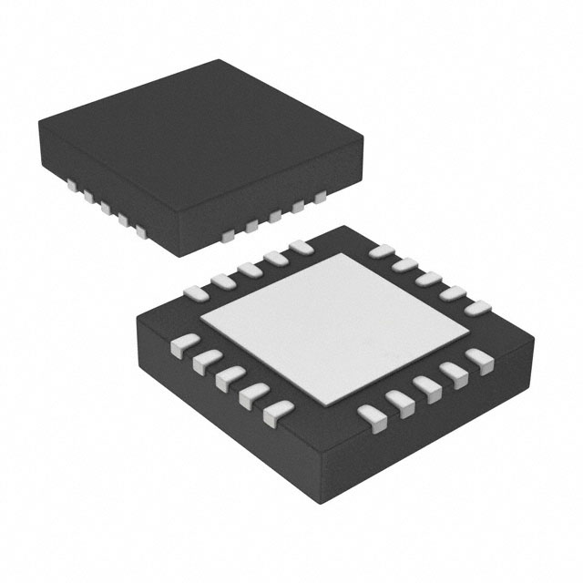
The UCS2113 is available in a 4x4 mm 20-pin QFN
package.
Package Type
ALERT#1
GND
SMDATA
SMCLK
ALERT#2
UCS2113
4 x 4 QFN*
20
19
18
17
16
PWR_EN1 1
15 PWR_EN2
GND 2
14 GND
EP
21
BOOST# 3
13 COMM_ILIM
7
8
9
10
VS
6
VS
11 VBUS2
VDD
VBUS1 5
VS
12 VBUS2
VS
VBUS1 4
* Includes Exposed Thermal Pad (EP); see Table 3-1.
2016 Microchip Technology Inc.
DS20005680A-page 1
�UCS2113
Block Diagram
VBUS
VS
Power
Switch 1
UVLO,
OVLO
VS
VBUS
Power
Switch 2
VBUS
discharge
PWR_EN1
Temp
BOOST#
VDD
Interface Logic
ALERT#1
Charger
Control,
Measurement,
OCL
PWR_EN2
ALERT#2
COMM_ILIM
SMCLK
GND
DS20005680A-page 2
SMDATA
2016 Microchip Technology Inc.
�UCS2113
1.0
ELECTRICAL
CHARACTERISTICS
Absolute Maximum Ratings †
Voltage on VDD, VS, and VBUS pins ...................................................................................................................-0.3 to 6V
Pull-Up Voltage (VPULLUP) ..................................................................................................................... -0.3 to VDD + 0.3
Port Power Switch Current ..................................................................................................................... Internally limited
Voltage on any Other Pin to Ground ...................................................................................................-0.3 to VDD + 0.3V
Current on any Other Pin ..................................................................................................................................... ±10 mA
Package Power Dissipation ........................................................................................................................ See Table 1-1
Operating Ambient Temperature Range .................................................................................................-40°C to +105°C
Storage Temperature Range ..................................................................................................................-55°C to +150°C
† Notice: Stresses above those listed under “Maximum Ratings” may cause permanent damage to the device. This is
a stress rating only and functional operation of the device at those or any other conditions above those indicated in the
operation listings of this specification is not implied. Exposure to maximum rating conditions for extended periods may
affect device reliability.
TABLE 1-1:
POWER DISSIPATION SUMMARY
Package
JC
JA
Derating Factor
Above +25°C
High K
(Note)
20-pin QFN
4x4 mm
6 °C/W
41 °C/W
24.4 mW/°C
2193 mW
1095 mW
729 mW
Low K
(Note)
20-pin QFN
4x4 mm
6 °C/W
60 °C/W
16.67 mW/°C
1498 mW
748 mW
498 mW
Board
Note:
TA < +25°C
TA = +70°C
TA = +85°C
Power Rating Power Rating Power Rating
A High-K board uses a thermal via design with the thermal landing soldered to the PCB ground plane with
0.3 mm (12 mil) diameter vias in a 3x3 matrix (9 total) at 0.5 mm (20 mil) pitch. The board is multilayer with
1-ounce internal power and ground planes and 2-ounce copper traces on top and bottom. A Low-K board
is a two-layer board without thermal via design with 2-ounce copper traces on the top and bottom.
TABLE 1-2:
ELECTRICAL SPECIFICATIONS
Electrical Characteristics: Unless otherwise specified, VDD = 4.5V to 5.5V, VS = 2.9V to 5.5V,
VPULLUP = 3V to 5.5V, TA = -40°C to 105°C. All typical values at VDD = VS = 5V, TA = 27°C.
Characteristic
Symbol
Min.
Typ.
Max.
Unit
Conditions
VDD
4.5
5
5.5
V
Supply Current in Active
(IDD_ACT + IS1_ACT + IS2_ACT)
IACTIVE
—
700
—
µA
Average current IBUS = 0 mA
Supply Current in Sleep
(IDD_SLEEP + IS1_SLEEP +
IS2_SLEEP)
ISLEEP
—
6
20
µA
Average current VPULLUP VDD
Power and Interrupts - DC
Supply Voltage
Power-On Reset
VDD Low Threshold
VDD_TH
—
4
4.3
V
VDD voltage increasing (Note 1)
VDD Low Hysteresis
VDD_TH_HYST
—
500
600
mV
VDD voltage decreasing (Note 1)
Note 1:
2:
3:
This parameter is characterized, not 100% tested.
This parameter is ensured by design and not 100% tested.
The current measurement full scale range maximum value is 3.4A. However, the UCS2113 cannot report values above
ILIM (if IBUS_R2MIN ILIM) or above IBUS_R2MIN (if IBUS_R2MIN > ILIM and ILIM 1.6A).
2016 Microchip Technology Inc.
DS20005680A-page 3
�UCS2113
TABLE 1-2:
ELECTRICAL SPECIFICATIONS (CONTINUED)
Electrical Characteristics: Unless otherwise specified, VDD = 4.5V to 5.5V, VS = 2.9V to 5.5V,
VPULLUP = 3V to 5.5V, TA = -40°C to 105°C. All typical values at VDD = VS = 5V, TA = 27°C.
Characteristic
Symbol
Min.
Typ.
Max.
Unit
Conditions
I/O Pins - SMCLK, SMDATA, PWR_EN, ALERT#, BOOST# - DC Parameters
Output Low Voltage
VOL
—
—
0.4
V
ISINK_IO = 8 mA
SMDATA, ALERT#, BOOST#
Input High Voltage
VIH
2.0
—
—
V
PWR_EN, SMDATA, SMCLK
Input Low Voltage
VIL
—
—
0.8
V
PWR_EN, SMDATA, SMCLK
Leakage Current
ILEAK
—
—
±5
µA
Powered or unpowered
VPULLUP VDD
TA < 85°C (Note 1)
ALERT# Pin Blanking Time
tBLANK
—
25
—
ms
Blanking time, coming out of
reset
ALERT# Pin Interrupt
Masking Time
tMASK
—
5
—
ms
BOOST# Pin Minimum
Assertion Time
tBOOST_MAT
—
1
—
s
BOOST# Pin Assertion
Current
IBOOST
—
1.9
—
A
Input Capacitance
CIN
—
5
—
pF
Clock Frequency
fSMB
10
—
400
kHz
tSP
—
—
50
ns
Interrupt Pins - AC Parameters
SMBus/I2C Timing
Spike Suppression
Bus Free Time Stop to Start
tBUF
1.3
—
—
µs
tSU:STA
0.6
—
—
µs
Start Hold Time
tHD:STA
0.6
—
—
µs
Stop Setup Time
tSU:STO
0.6
—
—
µs
Data Hold Time
tHD:DAT
0
—
—
µs
When transmitting to the master
Data Hold Time
tHD:DAT
0.3
—
—
µs
When receiving from the master
Data Setup Time
tSU:DAT
0.6
—
—
µs
Clock Low Period
tLOW
1.3
—
—
µs
Clock High Period
tHIGH
0.6
—
—
µs
Clock/Data Fall Time
tFALL
—
—
300
ns
Min. = 20+0.1CLOAD ns
(Note 1)
Clock/Data Rise Time
tRISE
—
—
300
ns
Min. = 20+0.1CLOAD ns
(Note 1)
Start Setup Time
Capacitive Load
Timeout
Idle Reset
Note 1:
2:
3:
CLOAD
—
—
400
pF
Per bus line (Note 1)
tTIMEOUT
25
—
35
ms
Disabled by default (Note 1)
tIDLE_RESET
350
—
—
µs
Disabled by default (Note 1)
This parameter is characterized, not 100% tested.
This parameter is ensured by design and not 100% tested.
The current measurement full scale range maximum value is 3.4A. However, the UCS2113 cannot report values above
ILIM (if IBUS_R2MIN ILIM) or above IBUS_R2MIN (if IBUS_R2MIN > ILIM and ILIM 1.6A).
DS20005680A-page 4
2016 Microchip Technology Inc.
�UCS2113
TABLE 1-2:
ELECTRICAL SPECIFICATIONS (CONTINUED)
Electrical Characteristics: Unless otherwise specified, VDD = 4.5V to 5.5V, VS = 2.9V to 5.5V,
VPULLUP = 3V to 5.5V, TA = -40°C to 105°C. All typical values at VDD = VS = 5V, TA = 27°C.
Characteristic
Symbol
Min.
Typ.
Max.
Unit
Conditions
Port Power Switch
Port Power Switch - DC Parameter
VS_OV
—
6
—
V
Note 2
VS Low Threshold
Overvoltage Lockout
VS_UVLO
—
2.5
—
V
Note 2
VS Low Hysteresis
VS_UVLO_HYST
—
100
—
mV
Note 2
On Resistance
RON_PSW
—
40
—
m
4.75V < VS < 5.25V
VS Leakage Current
ILEAK_VS
—
—
5
µA
Sleep state into VS pin on one
channel (Note 1)
Back-Voltage Protection
Threshold
VBV_TH
—
150
—
mV
VBUS > VS
VS > VS_UVLO
Leakage Current
ILKG_1
—
0
3
µA
VDD < VDD_TH,
Leakage current from VBUS pins
to the VDD and the VS pins
(Note 1)
ILKG_2
—
0
2
µA
VDD > VDD_TH,
Leakage current from VBUS pins
to the VS pins, when the power
switch is open
ILIM1
—
530
—
mA
ILIM Resistor = 0 or 47 k
(530 mA setting)
ILIM2
—
960
—
mA
ILIM Resistor = 10 k or 56 k
(960 mA setting)
ILIM3
—
1070
—
mA
ILIM Resistor = 12 k or 68 k
(1070 mA setting)
ILIM4
—
1280
—
mA
ILIM Resistor = 15 k or 82 k
(1280 mA setting)
ILIM5
—
1600
—
mA
ILIM Resistor = 18 k or 100 k
(1600 mA setting)
ILIM6
—
2130
—
mA
ILIM Resistor = 22 k or 120 k
(2130 mA setting)
ILIM7
2500
2670
2900
mA
ILIM Resistor = 27 k or 150 k
(2670 mA setting)
ILIM8
3000
3200
3400
mA
ILIM Resistor = 33 k or VDD
(3200 mA setting)
tPIN_WAKE
—
3
—
ms
SMBus Wake Time
tSMB_WAKE
—
4
—
ms
Idle Sleep Time
tIDLE_SLEEP
—
200
—
ms
First Thermal Shutdown
Stage Threshold
TTSD_LOW
—
120
—
°C
Die Temperature at which the
power switch will open if it is in
constant current mode
First Thermal Shutdown
Stage Hysteresis
TTSD_LOW_HYST
—
10
—
°C
Hysteresis for TTSD_LOW functionality. Temperature must drop
by this value before any of the
power switches can be closed.
Selectable Current Limits
Pin Wake Time
Note 1:
2:
3:
This parameter is characterized, not 100% tested.
This parameter is ensured by design and not 100% tested.
The current measurement full scale range maximum value is 3.4A. However, the UCS2113 cannot report values above
ILIM (if IBUS_R2MIN ILIM) or above IBUS_R2MIN (if IBUS_R2MIN > ILIM and ILIM 1.6A).
2016 Microchip Technology Inc.
DS20005680A-page 5
�UCS2113
TABLE 1-2:
ELECTRICAL SPECIFICATIONS (CONTINUED)
Electrical Characteristics: Unless otherwise specified, VDD = 4.5V to 5.5V, VS = 2.9V to 5.5V,
VPULLUP = 3V to 5.5V, TA = -40°C to 105°C. All typical values at VDD = VS = 5V, TA = 27°C.
Characteristic
Symbol
Min.
Typ.
Max.
Unit
Second Thermal Shutdown
Stage Threshold
TTSD_HIGH
—
135
—
°C
Die Temperature at which both
power switches will open
Second Thermal Shutdown
Stage Hysteresis
TTSD_HIGH_HYST
—
25
—
°C
Hysteresis for TTSD_HIGH
functionality. Temperature must
drop by this value before any of
the power switches can be
closed.
Auto-Recovery Test Current
ITEST
—
190
—
mA
Portable device attached,
VBUS= 0 V, Die temp < TTSD
Auto-Recovery Test Voltage
VTEST
—
750
—
mV
Portable device attached,
VBUS = 0 V before application,
Die temp < TTSD
Programmable, 250 - 1000 mV,
default listed
RDISCHARGE
—
100
—
Discharge Impedance
Conditions
Port Power Switch - AC Parameters
Turn-On Delay
tON_PSW
—
0.9
—
ms
PWR_EN active toggle to
switch on time, VBUS discharge
not active
Turn-Off Time
tOFF_PSW_INA
—
0.75
—
ms
PWR_EN inactive toggle to
switch off time
CBUS = 120 µF
Turn-Off Time
tOFF_PSW_ERR
—
1
—
ms
Over-current Error, VBUS Min
Error, or Discharge Error to
switch off
CBUS = 120 µF
Turn-Off Time
tOFF_PSW_ERR1
—
100
—
ns
TSD or Back-drive Error to
switch off
CBUS = 120 µF
tR_BUS
—
1.1
—
ms
Measured from 10% to 90% of
VBUS, CLOAD = 220 µF
ILIM = 1.0A
Soft Turn-On Rate
IBUS/t
—
100
—
mA/µs
Temperature Update Time
tDC_TEMP
—
200
—
ms
Short-Circuit Response Time
tSHORT_LIM
—
1.5
—
µs
Time from detection of short to
current limit applied.
No CBUS applied
Short-Circuit Detection Time
tSHORT
—
6
—
ms
Time from detection of short to
port power switch disconnect
and ALERT# pin assertion
tUL
—
7
—
ms
From PWR_EN edge transition
from inactive to active to begin
error recovery
VBUS Output Rise Time
Latched Mode Cycle Time
Note 1:
2:
3:
This parameter is characterized, not 100% tested.
This parameter is ensured by design and not 100% tested.
The current measurement full scale range maximum value is 3.4A. However, the UCS2113 cannot report values above
ILIM (if IBUS_R2MIN ILIM) or above IBUS_R2MIN (if IBUS_R2MIN > ILIM and ILIM 1.6A).
DS20005680A-page 6
2016 Microchip Technology Inc.
�UCS2113
TABLE 1-2:
ELECTRICAL SPECIFICATIONS (CONTINUED)
Electrical Characteristics: Unless otherwise specified, VDD = 4.5V to 5.5V, VS = 2.9V to 5.5V,
VPULLUP = 3V to 5.5V, TA = -40°C to 105°C. All typical values at VDD = VS = 5V, TA = 27°C.
Characteristic
Auto-Recovery Mode Cycle
Time
Auto-Recovery Delay
Discharge Time
Symbol
Min.
Typ.
Max.
Unit
Conditions
tCYCLE
—
25
—
ms
Time delay before error
condition check.
Programmable 15-50 ms,
default listed
tTST
—
20
—
ms
Portable device attached, VBUS
must be > VTEST after this time.
Programmable 10-25 ms,
default listed
tDISCHARGE
—
200
—
ms
Amount of time discharge
resistor applied.
Programmable 100-400 ms,
default listed
Port Power Switch Operation With Trip Mode Current Limiting
Region 2 Current
Keep-Out
IBUS_R2MIN_1
—
—
0.1
A
Note 2
Minimum VBUS
Allowed at Output
VBUS_MIN_1
2.0
—
—
V
Note 2
Port Power Switch Operation With Constant Current Limiting (Variable Slope)
Region 2 Current
Keep-Out
IBUS_R2MIN
—
—
2.13
A
Note 2
Minimum VBUS
Allowed at Output
VBUS_MIN
2.0
—
—
V
Note 2
IBUS_M
0
—
3400
mA
Range (Note 2 and Note 3)
IBUS_M
—
13.3
—
mA
1 LSB
—
±2
—
%
—
±2
—
LSB
Current Measurement - DC
Current Measurement Range
Reported Current
Measurement Resolution
Current Measurement
Accuracy
200 mA < IBUS < ILIM
IBUS < 200 mA
Current Measurement - AC
Sampling Rate
Conversion Time
Both Channels
—
—
1.1
—
ms
Note 2
tCONV
—
2.2
—
ms
All registers updated in digital
(Note 2)
—
—
±4.5
—
%
—
1
—
s
Charge Rationing - DC
Accumulated Current
Measurement Accuracy
Charge Rationing - AC
Current Measurement
Update Time
Note 1:
2:
3:
tPCYCLE
This parameter is characterized, not 100% tested.
This parameter is ensured by design and not 100% tested.
The current measurement full scale range maximum value is 3.4A. However, the UCS2113 cannot report values above
ILIM (if IBUS_R2MIN ILIM) or above IBUS_R2MIN (if IBUS_R2MIN > ILIM and ILIM 1.6A).
2016 Microchip Technology Inc.
DS20005680A-page 7
�UCS2113
T LOW
T HD:STA
T HIGH
T SU:STO
T FALL
SMCLK
T RISE
T HD:STA
T SU:DAT
T HD:DAT
T SU:STA
SMDATA
TBUF
S
P
FIGURE 1-1:
TABLE 1-3:
S
S - Start Condition
P - Stop Condition
P
SMBus Timing.
TEMPERATURE SPECIFICATIONS
Parameters
Sym.
Min.
Typ.
Max.
Units
Conditions
Temperature Ranges
Operating Temperature Range
TA
-40
—
+105
°C
Operating Junction Temperature
TJ
-40
—
+125
°C
Storage Temperature Range
TA
-55
—
+150
°C
Thermal Package Resistances - see Table 1-1
DS20005680A-page 8
2016 Microchip Technology Inc.
�UCS2113
1.1
ESD and Transient Performance
TABLE 1-4:
ESD RATINGS
ESD Specification
Rating or Value
Human Body Model (JEDEC JESD22-A114) - All pins
8 kV
Charged Device Model (JEDEC JESD22-C101) - All pins
500V
1.1.1
HUMAN BODY MODEL (HBM)
PERFORMANCE
HBM testing verifies the ability to withstand ESD
strikes, like those that occur during handling and
manufacturing, and is done without power applied to
the IC. To pass the test, the device must have no
change in operation or performance due to the event.
1.1.2
CHARGED DEVICE MODEL (CDM)
PERFORMANCE
CDM testing verifies the ability to withstand ESD
strikes, like those that occur during handling and
assembly, with pick-and-place-style machinery and is
done without power applied to the IC. To pass the test,
the device must have no change in operation or
performance due to the event.
2016 Microchip Technology Inc.
DS20005680A-page 9
�UCS2113
NOTES:
DS20005680A-page 10
2016 Microchip Technology Inc.
�UCS2113
2.0
TYPICAL PERFORMANCE CURVES
Note:
The graphs and tables provided following this note are a statistical summary based on a limited number of
samples and are provided for informational purposes only. The performance characteristics listed herein
are not tested or guaranteed. In some graphs or tables, the data presented may be outside the specified
operating range (e.g., outside specified power supply range) and therefore outside the warranted range.
Note: Unless otherwise indicated, VDD = VS = 5V, TA = +27°C.
6
3
3
2
2
1
1
VBUS
0
-1
0
2
4
FIGURE 2-1:
Power-Up.
6
Time (ms)
8
Voltage (V)
4
IBUS
1
-1
10
0
3
2
IBUS
1
1
0
0
-1
-1
100
120
140
160
180
200
On Resistance (mΩ)
ALERT#
3
80
6
35
30
25
20
15
10
5
0
-40
-15
10
0,95
3
16
2
12
1
8
4
-1
110
85
110
Turn on time
0,9
Time (ms)
Current (A)
Voltage (V)
1
20
IBUS
85
28
24
0
60
FIGURE 2-5:
Power Switch On
Resistance vs. Temperature.
4
VBUS
35
Temperature (°C)
Power-Up Into a Short.
VS = VDD = 5V
ILIM = 2.13A (typical), short applied at 10 µs
5
500
VBUS Discharge Behavior.
Time (ms)
FIGURE 2-2:
400
40
4
60
300
45
5
4
40
200
FIGURE 2-4:
6
20
100
Time (ms)
VS = VDD
0
2
0
6
2
3
-1
Short Applied After
5
4
0
Current (A)
Voltage (V)
4
VBUS
5
5
Current (A)
5
Voltage (V)
6
6
VS = VDD = 5V
ILIM = 3A min (3.4A max), short applied at 2 ms
Turn off time
0,85
0,8
0,75
0
0,7
-2
-4
0
20
40
Time (µs)
0,65
0,6
-40
FIGURE 2-3:
Response.
-15
Internal Power Switch Short
2016 Microchip Technology Inc.
10
35
60
Temperature (°C)
FIGURE 2-6:
vs. Temperature.
Power Switch On/Off Time
DS20005680A-page 11
�UCS2113
6.10
6.08
6.06
6.04
6.02
6.00
5.98
5.96
5.94
5.92
5.90
5
4
VDD = 5V
3
Accuracy (%)
VS Threshold Voltage (V)
Note: Unless otherwise indicated, VDD = VS = 5V, TA = +27°C.
2
1
0
-1
-2
-3
-4
-40
-15
10
35
60
85
110
-5
0.0
0.5
1.0
1.5
Temperature (°C)
VS Overvoltage Threshold
800
3.0
2.9
2.8
2.7
2.6
2.5
2.4
2.3
2.2
2.1
2.0
2.5
3.0
IBUS Measurement
IDD + IS1 + IS2
700
VDD = 5V
Threshold
Hysteresis
600
IDD
500
400
IS1 + IS2
300
200
100
-40
-15
10
35
60
85
110
FIGURE 2-8:
vs. Temperature.
0%
0
-40
Temperature (°C)
Current Limit Accuracy %)
FIGURE 2-10:
Accuracy.
Supply Current (ȝA)
VS Threshold Voltage (V)
FIGURE 2-7:
vs. Temperature.
2.0
Current (A)
-15
10
35
60
85
110
Temperature (°C)
VS Undervoltage Threshold
FIGURE 2-11:
Active State Current vs.
Temperature (both channels on,
PWR_EN1 = PWR_EN2 = 1).
VS = VDD = 5V
ILIM = 3.0A min. (3.2A typ., 3.4A max.)
-2%
Note: The percentage is relative to the
maximum specification (3.4A)
-4%
-6%
-8%
-10%
-12%
-40
-15
10
35
60
85
110
Temperature (°C)
FIGURE 2-9:
vs. Temperature.
DS20005680A-page 12
Trip Current Limit Operation
2016 Microchip Technology Inc.
�UCS2113
14
60%
12
50%
10
Samples (%)
IDD + IS1 + IS2
8
6
IDD
4
40%
30%
20%
10%
IS1 + IS2
FIGURE 2-15:
Distribution(1).
60%
60%
50%
50%
40%
40%
Samples (%)
30%
20%
10%
ILIM3 Trip Current
30%
20%
10%
1.33
1.675
1.31
1.3
1.29
1.28
1.27
1.32
FIGURE 2-13:
Distribution.
1.66
VBUS Current (A)
1.26
1.25
1.23
0.555
0.55
0.54
0.545
0.535
0.53
0.525
0.52
0.515
0.51
0.505
0%
1.24
VBUS Current (A)
FIGURE 2-16:
Distribution(1).
ILIM1 Trip Current
60%
50%
50%
40%
40%
Samples (%)
60%
30%
20%
10%
ILIM4 Trip Current
30%
20%
10%
ILIM2 Trip Current
1.645
1.63
1.615
1.6
1.585
VBUS Current (A)
VBUS Current (A)
FIGURE 2-14:
Distribution(1).
1.555
1.54
1.01
1
0.99
0.98
0.97
0.96
0.95
0.94
0.93
0.92
0.91
1.525
0%
0%
1.57
Samples (%)
Sleep State Current vs.
0%
Samples (%)
1.12
VBUS Current (A)
Temperature (°C)
FIGURE 2-12:
Temperature.
1.11
110
1.1
85
1.09
60
1.08
35
1.07
10
1.06
-15
1.02
-40
1.05
0%
0
1.04
2
1.03
Supply Current (ȝA)
Note: Unless otherwise indicated, VDD = VS = 5V, TA = +27°C.
FIGURE 2-17:
Distribution(1).
ILIM5 Trip Current
Note 1: The histogram aspect is caused by a mixture of two normal distributions, corresponding to the two
VBUS channels.
2016 Microchip Technology Inc.
DS20005680A-page 13
�UCS2113
Note: Unless otherwise indicated, VDD = VS = 5V, TA = +27°C.
60%
Samples (%)
50%
40%
30%
20%
10%
2.21
2.23
2.77
2.795
3.36
3.4
2.19
2.17
2.15
2.13
2.11
2.09
2.07
2.05
2.03
0%
VBUS Current (A)
FIGURE 2-18:
Distribution.
ILIM6 Trip Current
60%
Samples (%)
50%
40%
30%
20%
10%
2.745
2.72
2.695
2.67
2.645
2.62
2.595
2.57
2.545
0%
VBUS Current (A)
FIGURE 2-19:
Distribution.
ILIM7 Trip Current
60%
Samples (%)
50%
40%
30%
20%
10%
3.32
3.28
3.24
3.2
3.16
3.12
3.08
3.04
3
0%
VBUS Current (A)
FIGURE 2-20:
Distribution.
ILIM8 Trip Current
Note 1: The histogram aspect is caused by a mixture of two normal distributions, corresponding to the two
VBUS channels.
DS20005680A-page 14
2016 Microchip Technology Inc.
�PIN DESCRIPTION
Descriptions of the pins are listed in Table 3-1.
TABLE 3-1:
PIN FUNCTION TABLE
UCS2113
4x4 QFN
Symbol
1
PWR_EN1
Function
Port power switch enable #1
Ground
Pin Type
Connection Type if Pin Not Used
DI
Connect to ground or VDD
(depending on the polarity decoded via
COMM_ILIM pin)
2
GND
3
BOOST#
Logic output for DC-DC converter voltage increase (requires
pull-up resistor)
OD
4, 5
VBUS1
Port power switch #1 output (requires both pins tied together)
High Power, AIO
Leave open
6, 7
VS
Voltage input to port power switch VBUS1 (requires both pins
tied together)
High Power, AIO
Connect to ground
8
VDD
9, 10
VS
Common supply voltage
Power
Power
Voltage input to port power switch VBUS2 (requires both pins
tied together)
High Power, AIO
N/A
Connect to ground
N/A
Connect to ground
11, 12
VBUS2
Port power switch #2 output (requires both pins tied together)
High Power, AIO
13
COMM_ILIM
Enables SMBus or Stand-Alone mode at power-up. Hardware
strap for maximum current limit.
AIO
N/A
Power
N/A
2016 Microchip Technology Inc.
14
GND
15
PWR_EN2
Port power switch enable #2
DI
Connect to ground or VDD
(depending on the polarity decoded via
COMM_ILIM pin)
16
ALERT#2
Output fault ALERT for VBUS2 (requires pull-up resistor)
OD
Connect to ground
17
SMCLK
SMCLK - SMBus clock input (requires pull-up resistor)
DI
Connect to VPULLUP(or to ground in
Stand-Alone mode)
18
SMDATA
SMDATA - SMBus data input/output (requires pull-up resistor)
DIOD
Connect to VPULLUP (or to ground in
Stand-Alone mode)
Ground
Power
19
GND
20
ALERT#1
21
EP
Ground
Leave open
N/A
Output fault ALERT for VBUS1 (requires pull-up resistor)
OD
Connect to ground
Exposed thermal pad. Must be connected to electrical ground.
EP
N/A
UCS2113
DS20005680A-page 15
3.0
�UCS2113
TABLE 3-2:
PIN TYPES
Pin Type
Power
Description
This pin is used to supply power or
ground to the device
Hi-Power This pin is a high-current pin
AIO
Analog Input/Output - this pin is used as
an I/O for analog signals
DI
Digital Input - this pin is used as a digital
input
DIOD
Open-Drain Digital Input/Output - this
pin is bidirectional. It is open-drain and
requires a pull-up resistor.
OD
Open-Drain Digital Output - used as a
digital output. It is open-drain and
requires a pull-up resistor.
EP
Exposed thermal pad
DS20005680A-page 16
2016 Microchip Technology Inc.
�UCS2113
4.0
TERMS AND ABBREVIATIONS
Note:
The PWR_EN1 and PWR_EN2 pins each have configuration bits (“_S” in General
Configuration 1 register (Address 11h) and General Configuration 2 register (Address 12h)) that may be
used to perform the same function as the external pin state. These bits are accessed via the SMBus/I2C
and are OR’d with the respective pin. This OR’d combination of pin state and register bit is referenced as
the control.
TABLE 4-1:
TERMS AND ABBREVIATIONS
Term/Abbreviation
Description
CC
Constant Current
Current Limiting
Mode
Determines the action that is performed when the IBUS current reaches the ILIM threshold. Trip
opens the port power switch. Constant Current (variable slope) allows VBUS to be dropped by
the portable device.
IBUS_R2MIN
Current limiter mode boundary
ILIM
The IBUS current threshold used in current limiting. In Trip mode, when ILIM is reached, the
port power switch is opened. In Constant Current mode, when the current exceeds ILIM,
operation continues at a reduced voltage and increased current; if VBUS voltage drops below
VBUS_MIN, the port power switch is opened.
OCL
Overcurrent limit
POR
Power-on Reset
Portable Device
USB device attached to the USB port
Stand-Alone Mode
Indicates that the communications protocol is not active and all communications between the
UCS2113 and a controller are done via the external pins only (PWR_EN1 and PWR_EN2 as
inputs, and ALERT1# and ALERT2# as outputs)
2016 Microchip Technology Inc.
DS20005680A-page 17
�UCS2113
NOTES:
DS20005680A-page 18
2016 Microchip Technology Inc.
�UCS2113
5.0
GENERAL DESCRIPTION
The UCS2113 is a dual-port power switch. Two USB
power ports are supported with current limits up to 3.0A
continuous current (3.4A maximum) each. Selectable
and programmable current limiting configurations are
also available to the application. A typical block
diagram is shown in Figure 5-1.
D+
D-
SMDAT
SMCLK
VBUS
SMDAT
SMCLK
USB Port 1
Connector
VBUS1
D+
ALERT1
PWR_EN1
DPD_ALERT1
UCS2113
VBUS2
ALERT2
PWR_EN2
2 PORT HUB
VBUS
D+
D+
D-
D-
PD_ALERT2
FIGURE 5-1:
USB Port 2
Connector
Typical USB Application.
2016 Microchip Technology Inc.
DS20005680A-page 19
�UCS2113
5.1
UCS2113 Power States
Power states are indicators of the device’s current
consumption in the system and the functionality of the
digital logic. Table 5-1 details the UCS2113 power
states.
TABLE 5-1:
POWER STATES DESCRIPTION
State
Off
Description
This power state is entered when the voltage at the VDD pin voltage is < VDD_TH. In this state, the device is
considered “off”. The UCS2113 will not retain its digital states and register contents nor respond to SMBus/I2C
communications. The port power switch will be off. See Section 5.1.1 “Off State Operation”.
Sleep
This is the lowest power state available. While in this state, the UCS2113 will retain digital functionality and wake
to respond to SMBus/I2C communications. See Section 5.1.2 “Sleep State Operation”.
Error
This power state is entered when a fault condition exists. Error power state is one or both channels in Fault
Handling. This state is updated as Priority One. The Interrupt Status Registers for each channel will update the
fault detected per channel. Only the channel that has detected a Fault will be affected since the other channel
can remain active if no fault is detected. See Section 5.1.4 “Error State Operation”.
Active
Active power State is one, or both channels active and sourcing current to the VBUS Port. This state is updated
as Priority Two. None of the channels have detected Fault. This power state provides full functionality. While in
this state, operations include activation of the port power switch, current limiting, and charge rationing. See
Section 5.1.3 “Active State Operation”.
Table 5-2 shows the settings for the various power
states, except Off and Error. If VDD < VDD_TH, the
UCS2113 is in the Off state.
TABLE 5-2:
POWER STATES CONTROL SETTINGS
Power
PWR_EN1 PWR_EN2
State
Behavior
Sleep
disabled
disabled
• All switches disabled
• VBUS will be near ground potential
• The UCS2113 wakes to respond to SMBus
communications
Active
enabled
disabled
• Port power switch is on for VBUS1
• VBUS2 pins are near ground potential or floating (Note 1)
disabled
enabled
• Port power switch is on for VBUS2
• VBUS1 pins are near ground potential or floating (Note 1)
enabled
enabled
• Port power switch is on for VBUS1 and VBUS2
Note 1:
5.1.1
If the bit EN_VBUS_DISCHG is '1', the VBUS is discharged automatically and VBUS is near ground
potential. If the bit EN_VBUS_DISCHG is '0' then the corresponding VBUS pins are floating (VBUS
discharge is controlled by the SMBus master).
OFF STATE OPERATION
The device will be in the Off state if VDD is less than
VDD_TH. When the UCS2113 is in the Off state, it will do
nothing and all circuitry will be disabled. Digital register
values are not stored and the device will not respond to
SMBus commands.
5.1.2
SLEEP STATE OPERATION
The PWR_EN1 and PWR_EN2 pins may be used to
cause the UCS2113 to enter/exit Sleep. These pins are
AND’ed for Sleep mode.
When the UCS2113 is in the Sleep state, the device will
be in its lowest power state. The port power switch will
be disabled. VBUS1 and VBUS2 will be near ground
DS20005680A-page 20
potential. The ALERT#1 and ALERT#2 pins will not be
asserted. If asserted prior to entering the Sleep state,
the ALERT# pin will be released. SMBus activity is limited to single byte read or write.
The first data byte read from the UCS2113 when it is in
the Sleep state will wake it; however, the data to be
read will return all 0’s and should be considered invalid.
This is a “dummy” read byte meant to wake the
UCS2113. Subsequent read or write bytes will be
accepted normally. After the dummy read, the
UCS2113 will be in a higher power state (see
Figure 5-2). After communication has not occurred for
tIDLE_SLEEP, the UCS2113 will return to Sleep.
2016 Microchip Technology Inc.
�UCS2113
SMBus Read
Dummy read returns invalid data
and places device in temporary
Read returns valid data
Active state
S 0101_1110 A 0001_0000 A S 0101_1111 A invalid dataN P
Power State
5.1.3
tSMB_WAKE
temporary Active state
(not all functionality available)
Sleep
FIGURE 5-2:
ACTIVE STATE OPERATION
• VS < VS_UVLO
• PWR_EN1 and PWR_EN2 are disabled.
ERROR STATE OPERATION
The UCS2113 will enter the Error state from the Active
state when any of the following events are detected:
• The maximum allowable internal die temperature
(TTSD_HIGH) has been exceeded.
• The TTSD_LOW die temperature has been
exceeded and any of the following conditions is
met:
•
•
•
•
•
- a power switch operates in constant current
mode
- PWR_EN1 and/or PWR_EN2 controls
transition from inactive to active.
- it is a power up situation and PWR_EN1
and/or PWR_EN2 pins are active.
An overcurrent condition has been detected.
An undervoltage condition on either VBUS pin has
been detected (see Section 5.3.4 “Undervoltage
Lockout on VS”).
A back-voltage condition has been detected (see
Section 5.3.2 “Back-voltage Detection”).
A discharge error has been detected.
An overvoltage condition on the VS pin.
TABLE 5-3:
tIDLE_SLEEP
Sleep
Wake from Sleep using SMBus Read.
Every time the UCS2113 enters the Active state, the
port power switches are closed. The UCS2113 cannot
be in the Active state (and therefore, the port power
switch cannot be turned on) if any of the following
conditions exist:
5.1.4
S 0101_1110 A 0001_0000 A S 0101_1111 A valid data N P
When the UCS2113 enters the Error state, the port
power switch will be disabled while the ALERT# pin is
asserted. It will remain off while in this power state. The
UCS2113 will leave this state as determined by the fault
handling selection.
With the Auto-recovery fault handler, after the tCYCLE
time period, the UCS2113 will check that all of the error
conditions have been removed.
If all of the error conditions have been removed, the
UCS2113 will return to the Active state.
If both PWR_EN1 and PWR_EN2 controls transition
from active to inactive while the UCS2113 is in the Error
state, the device will not enter the Sleep state. After the
fault has been removed, the UCS2113 will not automatically enter the Sleep state if the EN_VBUS_DISCHG
bit from the General Configuration 2 Register is not set
(default setting). To enter the Sleep state, the PWR_EN
pins must be toggled or an SMBus read register command must be sent.
5.2
Communication
The UCS2113 can operate in SMBus mode (see
Section 7.0 “System Management Bus Protocol”)
or Stand-Alone mode. The resistor connected to the
COMM_ILIM pin determines the operating mode and
the hardware-set ILIM setting, as shown in Table 5-3.
Unless connected to GND or VDD, the resistors in
Table 5-3 are external pull-down resistors.
The SMBus address is specified in Section 7.2
“SMBus Address and RD/WR Bit”.
COMMUNICATION DECODE
COMM_ILIM Pull Down
Resistor (±1%)
PWR_EN1 and
PWR_EN2 Polarity
ILIM (A)
Total ILIM (A)
(Note 1)
Communication
Mode
GND
Active-High
0.53
0.53 + 0.53
SMBUS
10 k
Active-High
0.96
0.96 + 0.96
SMBUS
12 k
Active-High
1.07
1.07 + 1.07
SMBUS
15 k
Active-High
1.28
1.28 + 1.28
SMBUS
18 k
Active-High
1.6
1.6 + 1.6
SMBUS
2016 Microchip Technology Inc.
DS20005680A-page 21
�UCS2113
TABLE 5-3:
COMMUNICATION DECODE (CONTINUED)
COMM_ILIM Pull Down
Resistor (±1%)
PWR_EN1 and
PWR_EN2 Polarity
ILIM (A)
Total ILIM (A)
(Note 1)
Communication
Mode
22 k
Active-High
2.13
2.13 + 2.13
SMBUS
27 k
Active-High
2.67
2.67 + 2.67
SMBUS
33 k
Active-High
3.2
3.2 + 3.2
SMBUS
47 k
Active-Low
0.53
0.53 + 0.53
Stand-Alone
56 k
Active-Low
0.96
0.96 + 0.96
Stand-Alone
68 k
Active-Low
1.07
1.07 + 1.07
Stand-Alone
82 k
Active-Low
1.28
1.28 + 1.28
Stand-Alone
100 k
Active-Low
1.6
1.6 + 1.6
Stand-Alone
120 k
Active-Low
2.13
2.13 + 2.13
Stand-Alone
150 k
Active-Low
2.67
2.67 + 2.67
Stand-Alone
VDD
Active-Low
3.2
3.2 + 3.2
Stand-Alone
Note 1:
5.3
5.3.1
The total maximum current depends on power dissipation characteristics of the design (see Table 1-1).
Supply Voltages
VDD SUPPLY VOLTAGE
The UCS2113 requires 4.5V to 5.5V to be present on
the VDD pin for core device functionality. Core device
functionality consists of maintaining register states and
wake-up upon SMBus/I2C query.
5.3.2
BACK-VOLTAGE DETECTION
The back-voltage detector is functional in all power
states (Sleep and Active).
When in Sleep, the UCS2113 will enter the Error state
from Sleep if a back-voltage condition was detected.
Whenever the following condition is true for either port,
the port power switch will be disabled and a
back-voltage event will be flagged. This will cause the
UCS2113 to enter the Error power state (see
Section 5.1.4 “Error State Operation”).
Note:
The VBUS voltage exceeds the VS and/or
the VDD pin voltage by VBV_TH and the
port power switch is closed. The port
power switch will be opened immediately.
If the condition lasts for longer than tMASK,
then the UCS2113 will enter the Error
state. Otherwise, the port power switch
will be turned on as soon as the condition
is removed.
DS20005680A-page 22
5.3.3
BACK-DRIVE CURRENT
PROTECTION
If a portable device is attached that is self-powered, it
may drive the VBUS port to its power supply voltage
level; however, the UCS2113 is designed such that
leakage current from the VBUS pins to the VDD and/or
the VS pin shall not exceed ILKG_1 (if the VDD and/or VS
voltage is zero) or ILKG_2 (if the VDD and/or VS voltage
exceeds VDD_TH and the power switch is open).
5.3.4
UNDERVOLTAGE LOCKOUT ON VS
The UCS2113 requires a minimum voltage (VS_UVLO)
be present on the VS pin for Active power state.
5.3.5
OVERVOLTAGE DETECTION AND
LOCKOUT ON VS
Both power switches will be disabled if the voltage on
any VS pin exceeds a voltage (VS_OV) for longer than
the specified time (tMASK). This will cause the device to
enter the Error state and both ALERT#1 and ALERT#2
pins will be asserted.
5.3.6
PWR_EN1 AND PWR_EN2 INPUT
The PWR_EN control affects the power state and enables
the port power switch to be turned on if conditions are met
(see Table 5-2). The port power switch cannot be closed
if PWR_EN is disabled. However, if PWR_EN is enabled,
the port power switch is not necessarily closed (see
Section 5.1.3 “Active State Operation”). In SMBus
mode, the PWR_EN1 and PWR_EN2 pins states will be
ignored by the UCS2113 if the PIN_IGN configuration bit
is set; otherwise, the PWR_EN1S and PWR_EN2S
configuration bits are checked along with the pins.
2016 Microchip Technology Inc.
�UCS2113
The UCS2113 is compatible with the Microchip hub
devices supporting single pin power control feature.
These hub devices have a single connection to the
PWR_EN and ALERT# pins of the UCS2113, which are
tied together in the application.
ALERT#1 AND ALERT#2 OUTPUT
PINS
The UCS2113 has two independent ALERT# out pins.
ALERT#1 is tied to the status of the VBUS1 pin.
ALERT#2 is tied to the status of the VBUS2 pin.
The ALERT# pin is an active-low open-drain interrupt
to the host controller. The ALERT# pin is asserted
when an error occurs. Also, when charge rationing is
enabled, the ALERT# pin is asserted by default when
the current rationing threshold is reached (as
determined by RATION_BEH). The ALERT# pin
is released when all error conditions that may assert
the ALERT# pin (such as an error condition and charge
rationing) have been removed or reset as necessary.
5.4.2
BOOST# OUTPUT PIN
5.0VOUT
PWR_EN1
1
GND
2
SMDATA/LOW_ILM
SMCLK/LOAD_SHARE
ALERT#2
17
16
5V OUT R 1
VOUT --------------------------------R4
GND
If R 1 R 3
18
R + R + R V
1
2
3
FB
5V OUT = -------------------------------------------------------R3
R2 + R 3 R 1 V FB
VOUT = -------------------------------------------------------R3 R4
5V
OUT R 1 R 1 V FB
V OUT = -------------------- – ------ -----------------------R4
R3
V FB
19
The UCS2113 provides a BOOST# output pin to
compensate for voltage drops during high loads. The
BOOST# pin is an active-low, open-drain output that
would be connected to a resistor in the DC-DC
converter’s feedback error voltage loop (see
Figure 5-3).
The
BOOST#
pin
is
asserted
when
VBUS Current > IBOOST. IBOOST typical value is 1.9A.
The BOOST# is OR’ed for both VBUS1 and VBUS2 ports.
When the BOOST# pin is asserted, it will remain in this
state for at least tBOOST_MAT (minimum assertion time).
ALERT#1
5.4.1
Discrete Output Pins
20
5.4
15
PWR_EN2
14
GND
R1
R4
DC-DC
Converter Block
FeedBack
R2
VFB
BOOST#
UCS2113
20-QFN 4 x 4 mm
13
COMM_ILIM
VBUS1
3
4
12
VBUS2
VBUS1
5
11
VBUS2
5.5
5.5.1
10
9
8
VS
VS
VDD
Boost# Pin Usage.
Discrete Input Pins
COMM_ILIM INPUT
The
COMM_ILIM
input
determines
the
communications mode, as shown in Table 6-1. This is
also the hardware strap for MAX Current Limit.
5.5.2
VS
GND FLAG
VS
FIGURE 5-3:
7
6
R3
GND
5.5.3
SMDATA
When used in Stand-Alone, this pin should be tied to
ground.
When the UCS2113 is configured for SMBus
communications, the SMDATA is the data input/output.
SMCLK
When operated in Stand-Alone mode, this pin should be
tied to ground. When the UCS2113 is configured for
SMBus communications, the SMCLK is the clock input.
2016 Microchip Technology Inc.
DS20005680A-page 23
�UCS2113
NOTES:
DS20005680A-page 24
2016 Microchip Technology Inc.
�UCS2113
6.0
USB PORT POWER SWITCH
To assure compliance to various charging
specifications, the UCS2113 contains a USB port
power switch that supports two current-limiting modes:
Trip and Constant current (variable slope). The current
limit (ILIM) is pin selectable (and may be updated via
the register set). The switch also includes soft start
circuitry and a separate short circuit current limit.
TABLE 6-1:
ILIM DECODE
COMM_ILIM PWR_EN1
Pulldown
and
Resistor
PWR_EN2
(±1%)
Polarity
ILIM (A)
Total ILIM
(A)
(Note 1)
GND
Active-High
0.53
0.53+0.53
10 kΩ
Active-High
0.96
0.96+0.96
12 kΩ
Active-High
1.07
1.07+1.07
15 kΩ
Active-High
1.28
1.28+1.28
18 kΩ
Active-High
1.6
1.6+1.6
22 kΩ
Active-High
2.13
2.13+2.13
CURRENT LIMIT SETTING
27 kΩ
Active-High
2.67
2.67+2.67
The UCS2113 hardware set current limit, ILIM, can be
one of eight values. This resistor value is read once
upon UCS2113 power-up. The current limit can be
changed via the SMBus/I2C after power-up; however,
the programmed current limit cannot exceed the hardware set current limit. Unless connected to VDD, the
resistors in Table 6-1 are pull-down resistors.
33 kΩ
Active-High
3.2
3.2+3.2
The port power switch is on in the Active state (except
when VBUS is discharging).
6.1
6.1.1
Current Limiting
At power-up, the communication mode (Stand-Alone
or SMBus/I2C) and hardware current limit (ILIM) are
determined via the pull-down resistor (or pull-up
resistor if connected to VDD) on the COMM_ILIM pin,
as shown in Table 6-1.
6.1.2
SHORT CIRCUIT OUTPUT
CURRENT LIMITING
Short circuit current limiting occurs when the output
current is above the selectable current limit (ILIMx).
This event will be detected and the current will
immediately be limited (within tSHORT_LIM time). If the
condition remains, the port power switch will flag an
Error condition and enter the Error state.
6.1.3
SOFT START
When the PWR_EN control changes states to enable the
port power switch, the UCS2113 invokes a soft start
routine for the duration of the VBUS rise time (tR_BUS).
This soft start routine will limit current flow from VS into
VBUS while it is active. This circuitry will prevent current
spikes due to a step in the portable device current draw.
In the case when a portable device is attached while the
PWR_EN pin is already enabled, if the bus current
exceeds ILIM, the UCS2113 current limiter will respond
within a specified time (tSHORT_LIM) and will operate
normally at this point. The CBUS capacitor will deliver the
extra current, if any, as required by the load change.
Active-Low
0.53
0.53+0.53
Active-Low
0.96
0.96+0.96
68 kΩ
Active-Low
1.07
1.07+1.07
82 kΩ
Active-Low
1.28
1.28+1.28
100 kΩ
Active-Low
1.6
1.6+1.6
120 kΩ
Active-Low
2.13
2.13+2.13
150 kΩ
Active-Low
2.67
2.67+2.67
VDD
Active-Low
3.2
3.2+3.2
Note 1:
6.1.4
The total maximum current depends on
power dissipation characteristics of the
design (see Table 1-1).
CURRENT LIMITING MODES
The UCS2113 current limiting has two modes: Trip and
Constant Current (variable slope). Either mode
functions at all times when the port power switch is
closed.
6.1.4.1
Trip Mode
When using Trip current limiting, the UCS2113 USB
port power switch functions as a low-resistance switch
and rapidly turns off if the current limit is exceeded.
While operating using Trip current limiting, the VBUS
output voltage will be held relatively constant (equal to
the VS voltage minus the RON x IBUS current) for all
current values up to the ILIM.
If the current drawn by a portable device exceeds ILIM,
the following occurs:
1.
2.
3.
2016 Microchip Technology Inc.
47 kΩ
56 kΩ
The port power switch will be turned off (Trip
action).
The UCS2113 will enter the Error state and
assert the ALERT# pin.
The fault handling circuitry will then determine
subsequent actions.
DS20005680A-page 25
�UCS2113
Figure 6-1 shows operation of current limits in Trip
mode with the shaded area representing the USB 2.0
specified VBUS range. Dashed lines indicate the port
power switch output will go to zero (e.g., Trip) when
ILIM is exceeded. Note that operation at all possible
values of ILIM are shown in Figure 6-1 for illustrative
purposes only; in actual operation only one ILIM can be
active at any time.
ILIM (Amps)
Operating 0.53
Current
5.25
0.96 1.07 1.28
1.6
2.13
2.67
3.2
5
4.75
= ILIM’s
Trip action
(ILIM = 0.53 A)
4
Figure 6-3 shows operation of current limits while
using CC mode. Unlike Trip mode, once IBUS current
exceeds ILIM, operation continues at a reduced voltage
and increased current. Note that the shaded area representing the USB 2.0 specified VBUS range is now
restricted to an upper current limit of IBUS_R2MIN. Note
that the UCS2113 will heat up along each load line as
voltage decreases. If the internal temperature exceeds
the TTSD_LOW threshold, the corresponding power
switch operating in constant current mode will open. If
the internal temperature exceeds the TTSD_HIGH
threshold, both power switches will open, regardless
of whether the power switch channels are in current
limit. Also note that when the VBUS voltage is brought
low enough (below VBUS_MIN), the port power switch
will open.
VBUS (Volts)
Trip action
(ILIM = 3.2 A)
ILIM (Amps)
3
0.53
0.96
1.28
1.6 2.13
2.67
3.2
5.25
IBUS_R2MIN
5
4.75
2
= ILIM’s
4
1
0
0.96 1.07 1.28
0.53
0
1.6
2.13
2.67
3.2
VBUS (Volts)
Power Switch Voltage and Current
Output go to Zero when ILIM is
Exceeded
Constant resistance
IBUS operation line 4
(ILIM = 1.6 A)
Constant resistance
IBUS operation line 1
(ILIM = 0.53 A)
3
2
IBUS (Amps)
FIGURE 6-1:
6.1.4.2
Current Limiting in Trip Mode.
1
Constant Current Limiting (Variable
Slope)
Constant current limiting is used when the current
drawn is greater than ILIM (and ILIM < 1.6A). In CC
mode, the port power switch allows the attached
portable device to reduce VBUS output voltage to less
than the input VS voltage while maintaining current
delivery. The V/I slope depends on the user set ILIM
value. This slope is held constant for a given ILIM
value.
This mode is specifically provided for devices that rely
on resistive means to reduce VBUS voltage for direct
battery charging or to allow portable devices a means
to “test” charger capacity. See Figure 6-2.
IBUS
VS
VBUS IBUS_R2MIN Example.
0
0.53
0
0.96
1.28
1.6
2.13
2.67
3.2
IBUS (Amps)
FIGURE 6-4:
Note:
ILIM < IBUS_R2MIN Example.
The CC mode of operation is possible only
up to 1.6A. As long as the value of ILIM is
less than the fixed port power profile
IBUS_R2MIN value, CC mode is possible.
Otherwise, the USB port power switch will
operate in Trip mode operation.
2016 Microchip Technology Inc.
DS20005680A-page 27
�UCS2113
6.3
Thermal Protection
The UCS2113 utilizes two-stage internal thermal
management. The first is triggered when the die
temperature exceeds TTSD_LOW threshold and the
second is triggered when the die temperature exceeds
TTSD_HIGH threshold.
6.3.0.1
THE FIRST THERMAL
SHUTDOWN STAGE (TTSD_LOW)
The first stage turns off the individual power switch
channel when the die temperature exceeds TTSD_LOW
threshold and a power switch operates in constant
current mode. It also causes the corresponding
channel to enter in error state and the corresponding
ALERT# pin will be asserted.
When an over-current condition appears, the power
switch operates in constant current mode for the
duration of tMASK time. Because of the increased
voltage drop across the switch, the die temperature
increases. If the die temperature exceeds TTSD_LOW
threshold before the expiration of the tMASK time, then
the power switch will open immediately.
If the TTSD_LOW threshold has been exceeded, but the
die temperature has not decreased below the
TTSD_LOW recovery threshold, then the power switch
cannot be closed when commanded by the PWR_EN1
or PWR_EN2 controls in the following situations:
• PWR_EN1 and/or PWR_EN2 controls transition
from inactive to active.
• it is a power up situation and PWR_EN1 and/or
PWR_EN2 pins are active.
In these situations, the corresponding channel will
enter in error state and the corresponding ALERT# pin
will be asserted.
The first thermal shutdown stage allows the two ports
to work independently, by preventing the die
temperature to increase during over-current conditions
and to exceed the maximum allowable temperature
(TTSD_HIGH).
The error state will persist and the power switches can
not be closed until the temperature is below
TTSD_LOW - TTSD_LOW_HYST.
DS20005680A-page 28
6.3.0.2
THE SECOND THERMAL
SHUTDOWN STAGE (TTSD_HIGH)
The second thermal protection stage turns off both
power switches when the die temperature exceeds
TTSD_HIGH threshold, regardless of whether the power
switch channels are in current limit. It also causes both
channels to enter in error state and both ALERT#1 and
ALERT#2 pins to be asserted.
The error state will persist and the power switches
cannot be closed until the temperature is below
TTSD_HIGH - TTSD_HIGH_HYST.
6.4
VBUS Discharge
When the EN_VBUS_DISCHG bit from General
Configuration 2 Register is set (by default it is not set),
the UCS2113 will discharge VBUS through an internal
100 resistor when at least one of the following
conditions occur:
• The PWR_EN control is disabled (triggered on the
inactive edge of the PWR_EN control).
• The VS voltage drops below a specified threshold
(VS_UVLO) that causes the port power switch to be
disabled.
• When commanded into the Sleep power state.
• Upon recovery from the Error state.
• When commanded via the SMBus in the Active
state.
When the automatic VBUS discharge circuitry is
activated, the UCS2113 will confirm that VBUS was
discharged at the end of the tDISCHARGE time. If the
VBUS voltage is not below the VTEST level, a discharge
error will be flagged (by setting the DISCH_ERR(1/2)
status bit) and the UCS2113 will enter the Error state.
When the EN_VBUS_DISCHG bit from General
Configuration 2 Register is not set (default setting), the
automatic VBUS discharges described above are
disabled. In this case, the SMBus master must set and
clear bits DISCHG_LOAD1 and DISCHG_LOAD2 from
the Current Limit Behavior Registers, to discharge the
VBUS1 and VBUS2. Setting the DISCHG_LOAD1 and
DISCHG_LOAD2 bits connects the internal 100
resistor to discharge the corresponding VBUS path.
This functionality doesn't use any timers. The
discharge time is controlled by the SMBus master,
which must clear this bit when its internal timer expires.
2016 Microchip Technology Inc.
�UCS2113
6.5
Charge Rationing Interactions
When charge rationing is active, regardless of the
specified behavior, the UCS2113 will function normally
until the charge rationing threshold is reached. Note
that charge rationing is only active when the UCS2113
is in the Active state. Changing the charge rationing
behavior will have no effect on the charge rationing
data registers. If the behavior is changed prior to
reaching the charge rationing threshold, this change
TABLE 6-2:
RATION_BEH
(1 or 2)
1
will occur and be transparent to the user. When the
charge rationing threshold is reached, the UCS2113
will take action as shown in Table 6-2. If the behavior
is changed after the charge rationing threshold has
been reached, the UCS2113 will immediately adopt
the newly programmed behavior, clearing the ALERT#
pin and restoring switch operation respectively (see
Table 6-4).
CHARGE RATIONING BEHAVIOR
Behavior
Actions Taken
Notes
0
0
0
Report
0
1
Report and
Disconnect
(default)
1.
2.
ALERT# pin asserted
Port power switch disconnected
All bus monitoring is still active.
Toggling the PWR_EN control will cause the
device to change power states as defined by the
registers; however, the port power switch will
remain off until the rationing circuitry is reset.
1
0
Disconnect
and
Go to Sleep
1.
Port power switch disconnected
Device will enter the Sleep
state
All VBUS and VS monitoring will be stopped.
Toggling the PWR_EN control will have no effect
on the power state until the rationing circuitry is
reset.
1
1
TABLE 6-3:
Ignore
ALERT# pin asserted.
2.
Take no further action
CHARGE RATIONING RESET BEHAVIOR
Behavior
Reset Actions
Report
1.
2.
3.
Reset the Total Accumulated Charge registers
Clear the RATION status bit
Release the ALERT# pin
Report and Disconnect
1.
2.
3.
4.
Reset the Total Accumulated Charge registers
Clear the RATION status bit
Release the ALERT# pin
Check the PWR_EN controls and enter the indicated power state if the controls
changed
Disconnect and
Go to Sleep
1.
2.
3.
Reset the Total Accumulated Charge registers
Clear the RATION status bit
Check the PWR_EN controls and enter the indicated power state if the controls
changed
Ignore
1.
2.
Reset the Total Accumulated Charge registers
Clear the RATION status bit
TABLE 6-4:
Previous
Behavior
Ignore
EFFECTS OF CHANGING RATIONING BEHAVIOR AFTER THRESHOLD REACHED
New Behavior
Report
Actions Taken
Assert ALERT# pin
Report and
Disconnect
1.
2.
Assert ALERT# pin
Open port power switch. See the Report and Disconnect (default) in
Table 6-2
Disconnect and
Go to Sleep
1.
2.
Open port power switch
Enter the Sleep state. See the Disconnect and Go to Sleep in Table 6-2
2016 Microchip Technology Inc.
DS20005680A-page 29
�UCS2113
TABLE 6-4:
Previous
Behavior
EFFECTS OF CHANGING RATIONING BEHAVIOR AFTER THRESHOLD REACHED
New Behavior
Report
Ignore
Report and
Disconnect
Actions Taken
Release ALERT# pin.
Open port power switch. See the Report and Disconnect (default) in Table 6-2.
Disconnect and
Go to Sleep
1.
2.
3.
Release the ALERT# pin
Open the port power switch
Enter the Sleep state. See the Disconnect and Go to Sleep in Table 6-2.
Ignore
1.
2.
Release the ALERT# pin
Check the PWR_EN controls and enter the indicated power state if the
controls changed
Report
Check the PWR_EN controls and enter the indicated power state if the controls
changed
Report and
Disconnect
Disconnect and
Go to Sleep
Disconnect
and Go to
Sleep
1.
2.
Release the ALERT# pin
Enter the Sleep state. See the Disconnect and Go to Sleep in Table 6-2.
Ignore
Check the PWR_EN controls and enter the indicated power state if the controls
changed
Report
1.
2.
Assert the ALERT# pin
Check the PWR_EN controls and enter the indicated power state if the
controls changed
Report and
Disconnect
1.
2.
Assert the ALERT# pin
Check the PWR_EN controls to determine the power state, then enter that
state, except that the port power switch will not be closed
If the RATION_EN control is set to ‘0’ prior to reaching
the charge rationing threshold, rationing will be
disabled and the Total Accumulated Charge registers
will be cleared. If the RATION_EN control is set to ‘0’
after the charge rationing threshold has been reached,
the following additional steps occur:
1.
2.
3.
RATION status bit will be cleared.
The ALERT# pin will be released if asserted by
the rationing circuitry and no other conditions
are present.
The PWR_EN controls are checked to
determine the power state.
Setting the RATION_RST control to ‘1’ will
automatically reset the Total Accumulated Charge
registers to 00_00h. If this is done prior to reaching the
charge rationing threshold, the data will continue to be
accumulated restarting from 00_00h. If this is done
after the charge rationing threshold is reached, the
UCS2113 will take action as shown in Table 6-3.
DS20005680A-page 30
2016 Microchip Technology Inc.
�UCS2113
6.6
Fault Handling Mechanism
Faults do not include:
• keep-out violations except VBUS_MIN.
• TTSD_LOW die temperature has been exceeded
and any of the following conditions are met:
- the power switch is closed at the time when
TTSD_LOW is reached and it is not in constant
current mode.
- the power switch remains open (PWR_EN1
and/or PWR_EN2 controls are not active).
The UCS2113 has two modes for handling faults:
• Latch (latch-upon-fault)
• Auto-recovery (automatically attempt to restore
the Active power state after a fault occurs).
If the SMBus is actively utilized, Auto-Recovery Fault
Handling is the default error handler as determined by
the LATCH_SET bit. Faults include overcurrent,
overvoltage (on VS), undervoltage (on VBUS),
back-voltage (VBUS to VS or VBUS to VDD), discharge
error, and maximum allowable internal die temperature
(TTSD_HIGH) exceeded. Fault conditions also include
the situations when TTSD_LOW die temperature has
been exceeded and any of the following conditions are
met:
6.6.1
When the LATCH_SET bit is low, Auto-Recovery Fault
Handling is used. When an error condition is detected,
the UCS2113 will immediately enter the Error state
and assert the ALERT# pin. Independently from the
host controller, the UCS2113 will wait a preset time
(tCYCLE), check error conditions (tTST), and restore
Active operation if the error condition(s) no longer
exist. If all other conditions that may cause the
ALERT# pin to be asserted have been removed, the
ALERT# pin will be released. Short-Circuit
Auto-Recovery example in Figure 6-6.
• a power switch operates in constant current mode
• PWR_EN1 and/or PWR_EN2 controls transition
from inactive to active.
• it is a power up situation and PWR_EN1 and/or
PWR_EN2 pins are active.
tCYCLE
VBUS
AUTO-RECOVERY FAULT
HANDLING
tTST
tCYCLE
tTST
VTEST
tDISCHARGE
SHORT
applied.
IBUS
ITEST
Short Detected. VBUS
discharged. Enter
Error state.
FIGURE 6-6:
6.6.2
Wait tCYCLE.
Check short
condition. Short
still present.
Return to Error
State.
ITEST
Wait tCYCLE.
Check short
condition. Short
removed.
Return to
normal
operation.
Error Recovery.
LATCHED FAULT HANDLING
When the LATCH_SET bit is high, latch fault handling
is used. When an error condition is detected, the
UCS2113 will enter the Error power state and assert
the ALERT# (1 or 2) pin. Upon command from the host
controller (by toggling the PWR_EN (1, or 2) pin
control from enabled to disabled or by clearing the
ERR bit via SMBus), the UCS2113 will check error
conditions once and restore Active operation if error
conditions no longer exist. If an error condition still
exists, the host controller is required to issue the
command again to check error conditions.
2016 Microchip Technology Inc.
If the ALERT# pin is asserted and the interrupt status
registers (addresses 03h or 04h) are not read, the
corresponding ALERT# pin remains asserted until the
corresponding PWR_EN pin is toggled.
If the ALERT# pin is asserted and the interrupt status
registers are read, the ALERT# pin will deassert, but
the UCS will remain in error state until the ERR bit is
cleared via SMBus or the PWR_EN pin is toggled.
DS20005680A-page 31
�UCS2113
NOTES:
DS20005680A-page 32
2016 Microchip Technology Inc.
�UCS2113
7.0
SYSTEM MANAGEMENT BUS
PROTOCOL
In SMBus mode, the UCS2113 communicates with a
host controller, such as a Microchip PIC®
microcontroller or hub, through the SMBus. The
SMBus is a two-wire serial communication protocol
between a computer host and its peripheral devices. A
detailed timing diagram is shown in Figure 1-1.
Stretching of the SMCLK signal is supported; however,
the UCS2113 will not stretch the clock signal.
7.1
SMBus Start Bit
7.6
SMBus Time-out
The UCS2113 includes an SMBus time-out feature. If
the clock is held at logic ‘0’ for tTIMEOUT, the device
can time out and reset the SMBus interface. The
SMBus interface can also reset if both the clock and
data lines are held at a logic ‘1’ for tIDLE_RESET.
Communication is restored with a start condition.
The time-out function defaults to disabled. It can be
enabled by clearing the DIS_TO bit in the General
Configuration 3 register (see Register 8-9).
7.7
SMBus and I2C Compliance
The SMBus Start bit is defined as a transition of the
SMBus Data line from a logic ‘1’ state to a logic ‘0’
state while the SMBus Clock line is in a logic ‘1’ state.
The major difference between SMBus and I2C devices
is highlighted here. For complete compliance
information, refer to the SMBus 2.0 specification and
Application Note 14.0.
7.2
• UCS2113 supports I2C fast mode at 400 kHz. This
covers the SMBus maximum time of 100 kHz.
• The minimum frequency for SMBus
communications is 10 kHz.
• The client protocol will reset if the clock is held low
longer than 30 ms. This time out functionality is
disabled by default in the UCS2113 and can be
enabled by clearing the DIS_TO bit. I2C does not
have a time out.
• Except when operating in Sleep, the client
protocol will reset if both the clock and the data
line are logic ‘1’ for longer than 200 µs (idle
condition). This function is disabled by default in
the UCS2113 and can be enabled by clearing the
DIS_TO bit. I2C does not have an idle condition.
• I2C devices do not support the Alert Response
Address functionality (which is optional for SMBus).
• I2C devices support block read and write
differently. I2C protocol allows for unlimited
number of bytes to be sent in either direction. The
SMBus protocol requires that an additional data
byte indicating number of bytes to read/write is
transmitted. The UCS2113 supports I2C
formatting only.
SMBus Address and RD/WR Bit
The SMBus Address Byte consists of the 7-bit client
address followed by the RD/WR indicator bit. If this
RD/WR bit is a logic ‘0’, the SMBus Host is writing
data to the client device. If this RD/WR bit is a logic ‘1’,
the SMBus Host is reading data from the client device.
The UCS2113 with the order code UCS2113-1-V/G4
has the SMBus address 57h - 1010_111(r/w).
Customers
should
contact
their
distributor,
representatives or field application engineer (FAE) for
additional SMBus addresses. Local sales offices are
also available to help customers. A list of sales offices
and locations is included in the back of this document.
7.3
SMBus Data Bytes
All SMBus Data bytes are sent most significant bit first
and composed of 8 bits of information.
7.4
SMBus ACK and NACK Bits
The SMBus client will acknowledge all data bytes that
it receives. This is done by the client device pulling the
SMBus Data line low after the 8th bit of each byte that
is transmitted. This applies to both the Write Byte and
Block Write protocols.
The Host will NACK (not acknowledge) the last data byte
to be received from the client by holding the SMBus data
line high after the 8th data bit has been sent. For the
Block Read protocol, the Host will ACK (acknowledge)
each data byte that it receives except the last data byte.
7.5
SMBus Stop Bit
The SMBus Stop bit is defined as a transition of the
SMBus Data line from a logic ‘0’ state to a logic ‘1’
state while the SMBus clock line is in a logic ‘1’ state.
When the UCS2113 detects an SMBus Stop bit and it
has been communicating with the SMBus protocol, it
will reset its client interface and prepare to receive
further communications.
2016 Microchip Technology Inc.
7.8
SMBus Protocols
The UCS2113 is SMBus 2.0-compatible and supports
Send Byte, Read Byte, Block Read, Receive Byte as
valid protocols as shown below. The UCS2113 also
supports the I2C block read and block write protocols.
The device supports Write Byte, Read Byte, and Block
Read/Block Write. All of the below protocols use the
convention in Table 7-1.
TABLE 7-1:
SMBUS PROTOCOL
Data Sent to Device
Data Sent to the Host
Data sent
Data sent
DS20005680A-page 33
�UCS2113
7.9
SMBus Write Byte
The Write Byte is used to write one byte of data to a
specific register as shown in Table 7-2.
TABLE 7-2:
WRITE BYTE PROTOCOL
START
Slave
Address
WR
ACK
Reg. Addr.
ACK
Register Data
ACK
STOP
1→0
YYYY_YYY
0
0
XXh
0
XXh
0
0→1
7.10
SMBus Read Byte
The Read Byte protocol is used to read one byte of
data from the registers as shown in Table 7-3.
TABLE 7-3:
READ BYTE PROTOCOL
START
Slave Address
WR
ACK
Register Address
ACK
1→0
YYYY_YYY
0
0
XXh
0
START
Slave Address
RD
ACK
Register Data
NACK
STOP
1 →0
YYYY_YYY
1
0
XXh
1
0→1
7.11
Block Write
The Block Write is used to write multiple data bytes to
a group of contiguous registers, as shown in Table 7-4.
It is an extension of the Write Byte Protocol.
Note:
The Block Write and Block Read protocols
require that the address pointer be automatically incremented. For a write command, the address pointer will be
automatically incremented when the ACK
is sent to the host. There are no over or
under bound limit checking and the
address pointer will wrap around from FFh
to 00h if necessary
TABLE 7-4:
START
1→0
7.12
BLOCK WRITE PROTOCOL
Slave Address
YYYY_YYY
WR
0
ACK
0
Register
Address
XXh
ACK
0
Repeat N Times
ACK
Register Data
XXh
0
STOP
0→1
Block Read
The Block Read is used to read multiple data bytes
from a group of contiguous registers, as shown in
Table 7-5. It is an extension of the Read Byte Protocol.
TABLE 7-5:
BLOCK READ PROTOCOL
START
Slave Address
WR
ACK
Register
Address
ACK
1→0
YYYY_YYY
0
0
XXh
0
START
Slave Address
RD
ACK
1→0
YYYY_YYY
1
0
DS20005680A-page 34
Repeat N Times
Register Data
ACK
XXh
0
Register Data NACK
XXh
1
STOP
0→1
2016 Microchip Technology Inc.
�UCS2113
7.13
SMBus Send Byte
The Send Byte protocol is used to set the internal
address register pointer to the correct address location.
No data is transferred during the Send Byte protocol as
shown in Table 7-6.
Note:
The SMBus Send Byte command is
expected to be followed by the SMBus
Receive Byte command. When two
SMbus Send Byte commands are sent in
a row, the first command receives an ACK
and will be processed by the UCS2113,
but the second command receives a
NACK and will be ignored.
TABLE 7-6:
SEND BYTE PROTOCOL
START
Slave Address
WR
ACK
Register Address
ACK
STOP
1→0
YYYY_YYY
0
0
XXh
0
0→1
7.14
SMBus Receive Byte
The Receive Byte protocol is used to read data from a
register when the internal register address pointer is
known to be at the right location (e.g. set via Send
Byte). This is used for consecutive reads of the same
register as shown in Table 7-7.
TABLE 7-7:
RECEIVE BYTE PROTOCOL
START
Slave Address
RD
ACK
Register Data
NACK
STOP
1→0
YYYY_YYY
1
0
XXh
1
0→1
7.14.1
STAND-ALONE OPERATING MODE
Stand-Alone mode allows the UCS2113 to operate
without
active
SMBus/I2C
communications.
Stand-Alone mode can be enabled by connecting a
pull-down resistor greater or equal to 47 k on the
COMM_ILIM pin as shown in Table 5-3.The SMCLK
pin should be tied to ground in this mode.
2016 Microchip Technology Inc.
DS20005680A-page 35
�UCS2113
NOTES:
DS20005680A-page 36
2016 Microchip Technology Inc.
�UCS2113
8.0
REGISTER DESCRIPTION
The registers shown in Table 8-1 are accessible
through the SMBus or I2C. An entry of ‘—’ indicates
that the bit is not used. Writing to these bits will have no
effect and reading these bits will return ‘0’. Writing to a
reserved bit may cause unexpected results and
reading from a reserved bit will return either ‘1’ or ‘0’ as
indicated in the bit description. While in the Sleep state,
the UCS2113 will retain configuration and charge
rationing data as indicated in the text. If a register does
not indicate that data will be retained in the Sleep
power state, this information will be lost when the
UCS2113 enters the Sleep power state.
TABLE 8-1:
Register
Address
00h
REGISTER SET IN HEXADECIMAL ORDER
Register Name
R/W
Default Page
Value
No.
Function
Port 1 Current Measurement
R
Stores the current measurement for Port 1
00h
38
01h
Port 2 Current Measurement
R
Stores the current measurement for Port 2
00h
38
02h
Port Status
R
Indicates Port and general status
00h
39
03h
Interrupt Status1
See Text
Indicates why ALERT# pin asserted for Port 1
00h
40
04h
Interrupt Status2
See Text
Indicates why ALERT# pin asserted for Port 2
00h
42
0Fh
General Status1
R/R-C
Indicates General Status for Port 1
00h
44
10h
General Status2
R/R-C
Indicates General Status for Port 2
00h
45
11h
General Configuration1
R/W
Controls basic functionality for Port 1
06h
46
12h
General Configuration2
R/W
Controls basic functionality for Port 2
02h
47
13h
General Configuration3
R/W
Controls other functionality
60h
48
14h
Current Limit
R/W
Controls/Displays MAX Current Limit per port
00h
49
15h
Auto-Recovery Configuration
R/W
Controls the Auto-Recovery functionality
2Ah
50
16h
Port 1 Total Accumulated
Charge High Byte
R
Stores the total accumulated charge
delivered high byte, Port 1
00h
51
17h
Port 1 Total Accumulated
Charge Middle High Byte
R
Stores the total accumulated charge
delivered middle high byte, Port 1
00h
51
18h
Port 1 Total Accumulated
Charge Middle Low Byte
R
Stores the total accumulated charge
delivered middle low byte, Port 1
00h
51
19h
Port 1 Total Accumulated
Charge Low Byte
R
Stores the total accumulated charge
delivered low byte, Port 1
00h
51
1Ah
Port 2 Total Accumulated
Charge High Byte
R
Stores the total accumulated charge
delivered high byte, Port 2
00h
52
1Bh
Port 2 Total Accumulated
Charge Middle High Byte
R
Stores the total accumulated charge
delivered middle high byte, Port 2
00h
52
1Ch
Port 2 Total Accumulated
Charge Middle Low Byte
R
Stores the total accumulated charge
delivered middle low byte, Port 2
00h
52
1Dh
Port 2 Total Accumulated
Charge Low Byte
R
Stores the total accumulated charge
delivered low byte, Port 2
00h
52
1Eh
Port 1 Charge Rationing
Threshold High Byte
R/W
Sets the maximum allowed charge that will
be delivered to Port 1
FFh
53
1Fh
Port 1 Charge Rationing
Threshold Low Byte
R/W
Sets the maximum allowed charge that will
be delivered to Port 1
FFh
53
20h
Port 2 Charge Rationing
Threshold High Byte
R/W
Sets the maximum allowed charge that will
be delivered to Port 2
FFh
53
2016 Microchip Technology Inc.
DS20005680A-page 37
�UCS2113
TABLE 8-1:
REGISTER SET IN HEXADECIMAL ORDER (CONTINUED)
Register
Address
Register Name
R/W
Default Page
Value
No.
Function
21h
Port 2 Charge Rationing
Threshold Low Byte
R/W
Sets the maximum allowed charge that will
be delivered to Port 2
FFh
53
22h
Ration Configuration
R/W
Controls Charge Ration Functionality
11h
54
23h
Port 1 Current Limit Behavior R/W
Controls the Current Limiting Behavior (CC
Mode Region 2) for Port 1
96h
55
24h
Port 2 Current Limit Behavior R/W
Controls the Current Limiting Behavior (CC
Mode Region 2) for Port 2
96h
55
FDh
Product ID
Stores a fixed value that identifies each
product
E1h
56
FEh
Manufacturer ID
R
Stores a fixed value that identifies Microchip
5Dh
56
FFh
Revision
R
Stores a fixed value that represents the
revision number
81h
57
8.1
R
Current Measurement Register
The Current Measurement register stores the
measured current value delivered to the portable
device (IBUS). This value is updated continuously while
the device is in the Active power state.
REGISTER 8-1:
R-0
PORTS 1 AND 2 CURRENT MEASUREMENT REGISTERS
(ADDRESSES 00H, 01H)
R-0
R-0
R-0
R-0
R-0
R-0
R-0
CM(x)
bit 7
bit 0
Legend:
R = Readable bit
W = Writable bit
U = Unimplemented bit
-n = Value at POR
‘1’ = Bit is set
‘0’ = Bit is cleared
bit 7-0
Note 1:
2:
x = Bit is unknown
CM(x): Port X Current Measurement, where x=1 or 2 (address 00h for Port 1 and address 01h for
Port 2).
The bit weights are in mA,1 LSB = 13.3 mA (maximum value is 255 LSB corresponding to 3.4A).
This data will be cleared when the device enters the Sleep state. This data will also be cleared whenever
the port power switch is turned off (or any time that VBUS is discharged).
DS20005680A-page 38
2016 Microchip Technology Inc.
�UCS2113
8.2
Status Registers
The Status registers store bits that indicate the state of
the ALERT# pins and if the ports operate in Constant
Current Mode.
REGISTER 8-2:
R-0
ALERT2_PIN
PORT STATUS REGISTER (ADDRESS 02H)
R-0
ALERT1_PIN
R-0
CC_MODE2
R-0
U-0
U-0
R-x
R-x
CC_MODE1
—
—
—
—
bit 7
bit 0
Legend:
R = Readable bit
W = Writable bit
U = Unimplemented bit
-n = Value at POR
‘1’ = Bit is set
‘0’ = Bit is cleared
x = Bit is unknown
bit 7
ALERT2_PIN: Reflects the status of the ALERT#2 pin. This bit is set and cleared as the ALERT#2 pin
changes states.
1 = ALERT#2 Pin asserted (logic low)
0 = ALERT#2 Pin not asserted
bit 6
ALERT1_PIN: Reflects the status of the ALERT#1 pin. This bit is set and cleared as the ALERT#1 pin
changes states.
1 = ALERT#1 Pin asserted (logic low)
0 = ALERT#1 Pin not asserted
bit 5
CC_MODE2: Port 2 Constant Current Mode State
1 = Port 2 in Constant Current mode
0 = Port 2 operating normally
bit 4
CC_MODE1: Port 1 Constant Current Mode State
1 = Port 1 in Constant Current mode
0 = Port 1 operating normally
bit 3-0
Unimplemented
2016 Microchip Technology Inc.
DS20005680A-page 39
�UCS2113
REGISTER 8-3:
INTERRUPT STATUS 1 REGISTER (ADDRESS 03H)
R/W-0
R/C-0
R/C-0
R/C-0
R/C-0
R/C-0
R/C-0
R/C-0
ERR1
DISCH_ERR1
RESET
KEEP_OUT1
TSD_HIGH
OV_VOLT
BACK_V1
OV_LIM1
bit 7
bit 0
Legend:
R = Readable bit
W = Writable bit
U = Unimplemented bit
C = Clear on Read
-n = Value at POR
‘1’ = Bit is set
‘0’ = Bit is cleared
x = Bit is unknown
bit 7
ERR1: Error Port 1 - Indicates that an error was detected on the VBUS1 pin and the device has entered
the Error state. Writing this bit to ‘0’ will clear the Error state and allows the device to be returned to the
Active state. When written to ‘0’, all error conditions are checked. If all error conditions have been
removed, the UCS2113 returns to the Active state. This bit is set automatically by the UCS2113 when
the Error state is entered. If any other bit is set in the Interrupt Status register (03h), the device will not
leave the Error state.
This bit is cleared automatically by the UCS2113 if the Auto-recovery fault handling functionality is active
and no error conditions are detected. Likewise, this bit is cleared when the PWR_EN1 control is disabled
(Note 1).
1 = Port 1 in Error State
0 = Port 1 in Active State (no errors detected)
bit 6
DISCH_ERR1: Discharge Error Port 1 - Indicates the device was unable to discharge Port1. This bit will
be cleared when read if the error condition has been removed or if the ERR bit is cleared. This bit will
cause the ALERT#1 pin to be asserted and the device to enter the Error state.
1 = UCS2113 was unable to Discharge VBUS1
0 = No VBUS1 discharge error
bit 5
RESET: Indicates that the UCS2113 has just been reset and should be reprogrammed. This bit will be
set at power-up. This bit is cleared when read or when the PWR_EN control is toggled. The ALERT#
pins are not asserted when this bit is set. This data is retained in the Sleep state.
1 = UCS2113 has just been reset
0 = Reset did not occur
bit 4
KEEP_OUT1: Port 1 Minimum Keep-Out region - Indicates that the V-I output on the VBUS1 pin has
dropped below VBUS_MIN. This bit will be cleared when read if the error condition has been removed or
if the ERR1 bit is cleared. This bit will cause the ALERT#1 pin to be asserted and the device to enter the
Error state.
1 = VBUS1 < VBUS_MIN
0 = VBUS1 > VBUS_MIN
bit 3
TSD_HIGH: Indicates that the internal temperature has exceeded TTSD_HIGH threshold and the device
has entered the Error state. This bit will be cleared when read if the error condition has been removed
or if the ERR1 bit is cleared. This bit will cause the ALERT#1and ALERT#2 pins to be asserted and the
device to enter the Error state.
1 = Internal die temperature has exceeded TTSD_HIGH
0 = Internal die temperature has not exceeded TTSD_HIGH
bit 2
OV_VOLT: VS Overvoltage indicates that the VS voltage has exceeded the VS_OV threshold, and the
device has entered the Error state. This bit will be cleared when read if the error condition has been
removed or if the ERR1 bit is cleared. This bit will cause the ALERT#1 and ALERT#2 pins to be asserted
and the device to enter the Error state.
1 = VS > VS_OV
0 = VS < VS_OV
DS20005680A-page 40
2016 Microchip Technology Inc.
�UCS2113
REGISTER 8-3:
INTERRUPT STATUS 1 REGISTER (ADDRESS 03H) (CONTINUED)
bit 1
BACK_V1: Back-Bias Voltage Port 1 - Indicates that the VBUS1 voltage has exceeded the VS or VDD
voltages by more than 150 mV. This bit will be cleared when read if the error condition has been removed
or if the ERR1 bit is cleared. This bit will cause the ALERT#1 pin to be asserted and the device to enter
the Error state.
1 = VBUS1 > VS, or VBUS1 > VDD by more than 150 mV.
0 = VBUS1 voltage has not exceeded the VS and VDD voltages by more than 150 mV.
bit 0
OV_LIM1: Over Current Limit Port 1 - Indicates that the IBUS current has exceeded both the ILIM threshold and the IBUS_R2MIN threshold settings for VBUS1. This bit will be cleared when read if the error condition has been removed or if the ERR1 bit is cleared. This bit will cause the ALERT#1 pin to be asserted
and the device to enter the Error state.
1 = Current Limit for Port 1 exceeded
0 = Current Limit for Port 1 not exceeded
Note 1:
Note that the ERR1 bit does not necessarily reflect the ALERT#1 pin status. The ALERT#1 pin may be
cleared or asserted without the ERR1 bit changing states.
2016 Microchip Technology Inc.
DS20005680A-page 41
�UCS2113
REGISTER 8-4:
INTERRUPT STATUS 2 REGISTER (ADDRESS 04H)
R/W-0
R/C-0
R-0
R/C-0
R/C-0
U-0
R/C-0
R/C-0
ERR2
DISCH_ERR2
VS_LOW
KEEP_OUT2
TSD_LOW
—
BACK_V2
OV_LIM2
bit 7
bit 0
Legend:
R = Readable bit
W = Writable bit
U = Unimplemented bit
C = Clear on Read
-n = Value at POR
‘1’ = Bit is set
‘0’ = Bit is cleared
x = Bit is unknown
bit 7
ERR2: Error Port 2 - Indicates that an error was detected on the VBUS1 pin and the device has entered
the Error state. Writing this bit to a ‘0’ will clear the Error state and allows the device to be returned to
the Active state. When written to ‘0’, all error conditions are checked. If all error conditions have been
removed, the UCS2113 returns to the Active state. This bit is set automatically by the UCS2113 when
the Error state is entered. If any other bit is set in the Interrupt Status register (04h), the device will not
leave the Error state. This bit is cleared automatically by the UCS2113 if the auto-recovery fault handling
functionality is active and no error conditions are detected. Likewise, this bit is cleared when the
PWR_EN2 control is disabled (Note 1).
1 = Port 2 in Error State
0 = Port 2 in Active State (no errors detected)
bit 6
DISCH_ERR2: Discharge Error Port 2 - Indicates the device was unable to discharge Port2. This bit will
be cleared when read if the error condition has been removed or if the ERR bit is cleared. This bit will
cause the ALERT#2 pin to be asserted and the device to enter the Error state.
1 = Device was unable to Discharge VBUS2
0 = No VBUS2 discharge error
bit 5
VS_LOW: Indicates that the VS voltage has fallen below the VS_UVLO threshold and both VBUS1 and
VBUS2 port power switches are held off. This bit is cleared automatically when the VS voltage is above
the VS_UVLO threshold.
1 = VS voltage has fallen below the VS_UVLO
0 = VS voltage is above VS_UVLO
bit 4
KEEP_OUT2: Port 2 Minimum Keep-out region - Indicates that the V-I output on the VBUS2 pin has
dropped below VBUS_MIN. This bit will be cleared when read if the error condition has been removed or
if the ERR2 bit is cleared. This bit will cause the ALERT#2 pin to be asserted and the device to enter the
Error state.
1 = VBUS2 < VBUS_MIN
0 = VBUS2 > VBUS_MIN
bit 3
TSD_LOW: Indicates that the die temperature has exceeded the TTSD_LOW threshold and it is still above
the TTSD_LOW - TTSD_LOW_HYST. This bit is cleared automatically when the die temperature is below
the TTSD_LOW -TTSD_LOW_HYST. This bit will not cause the corresponding ALERT#1 and/or
ALERT#2 pins to be asserted and ERR1 and/or ERR2 bits to be set unless:
• a power switch operates in constant current mode
• PWR_EN1 and/or PWR_EN2 controls transition from inactive to active
• it is a power up situation and PWR_EN1 and/or PWR_EN2 pins are active.
1 = Internal die temperature has exceeded TTSD_LOW
0 = Internal die temperature has not exceeded TTSD_LOW
bit 2
Unimplemented: Read as '0'
bit 1
BACK_V2: Back-Bias Voltage Port 2 - Indicates that the VBUS2 voltage has exceeded the VS or VDD
voltages by more than 150 mV. This bit will be cleared when read if the error condition has been removed
or if the ERR2 bit is cleared. This bit will cause the ALERT#2 pin to be asserted and the device to enter
the Error state.
1 = VBUS2 > VS, or VBUS2 > VDD by more than 150 mV
0 = VBUS2 voltage has not exceeded the VS and VDD voltages by more than 150 mV
DS20005680A-page 42
2016 Microchip Technology Inc.
�UCS2113
REGISTER 8-4:
bit 0
Note 1:
INTERRUPT STATUS 2 REGISTER (ADDRESS 04H) (CONTINUED)
OV_LIM2: Overcurrent Limit Port 2 - Indicates that the IBUS current has exceeded both the ILIM threshold
and the IBUS_R2MIN threshold settings for VBUS2. This bit will be cleared when read if the error condition
has been removed or if the ERR2 bit is cleared. This bit will cause the ALERT#2 pin to be asserted and
the device to enter the Error state.
1 = Current Limit for Port 2 exceeded
0 = Current Limit for Port 2 not exceeded
Note that the ERR2 bit does not necessarily reflect the ALERT#2 pin status. The ALERT#2 pin may be cleared or
asserted without the ERR2 bit changing states.
2016 Microchip Technology Inc.
DS20005680A-page 43
�UCS2113
REGISTER 8-5:
GENERAL STATUS 1 REGISTER (ADDRESS 0FH)
R/C-0
U-x
U-x
RATION1
—
—
R-0
R-0
CC_MODE1 PWR_EN1_CON
U-x
U-x
U-x
—
—
—
bit 7
bit 0
Legend:
R = Readable bit
W = Writable bit
U = Unimplemented bit
C = Clear on Read
-n = Value at POR
‘1’ = Bit is set
‘0’ = Bit is cleared
x = Bit is unknown
bit 7
RATION1: Indicates the state of Port 1 Rationing. This bit is cleared when read, or cleared automatically
when the RATION_RST1 bit is set or the RATION_EN1 bit is cleared.
1 = Port 1 has delivered the programmed mAh of current
0 = Port 1 has not delivered the programmed mAh of current
bit 6-5
Unimplemented
bit 4
CC_MODE1: Indicates whether Port 1 has entered CC mode.
1 = Port 1 is in CC mode
0 = Port 1 not in CC mode
bit 3
PWR_EN1_CON: Reflects the PWR_EN control state. This bit is set and cleared automatically with the
logic expression (PWR_EN1 pin OR PWR_EN1S).
1 = Port 1 Power Enable is set
0 = Port 1 Power Enable is clear
bit 2-0
Unimplemented
DS20005680A-page 44
2016 Microchip Technology Inc.
�UCS2113
REGISTER 8-6:
GENERAL STATUS 2 REGISTER (ADDRESS 10H)
R/C-0
U-x
U-x
RATION2
—
—
R-0
R-0
CC_MODE2 PWR_EN2_CON
U-x
U-x
U-x
—
—
—
bit 7
bit 0
Legend:
R = Readable bit
W = Writable bit
U = Unimplemented bit
C = Clear on Read
-n = Value at POR
‘1’ = Bit is set
‘0’ = Bit is cleared
x = Bit is unknown
bit 7
RATION2: Indicates the state of Port 2 Rationing. This bit is cleared when read, or cleared automatically
when the RATION_RST2 bit is set or the RATION_EN2 bit is cleared.
1 = Port 2 has delivered the programmed mAh of current
0 = Port 2 has not delivered the programmed mAh of current
bit 6-5
Unimplemented
bit 4
CC_MODE2: Indicates whether Port 2 has entered CC mode.
1 = Port 2 is in CC mode
0 = Port 2 not in CC mode
bit 3
PWR_EN2_CON: Reflects the PWR_EN control state. This bit is set and cleared automatically with the
logic expression (PWR_EN2 pin OR. PWR_EN2S).
1 = Port 2 Power Enable is set
0 = Port 2 Power Enable is clear
bit 2-0
Unimplemented
2016 Microchip Technology Inc.
DS20005680A-page 45
�UCS2113
8.3
Configuration Registers
The Configuration registers control basic device
functionality. The contents of these registers are
retained in Sleep.
REGISTER 8-7:
GENERAL CONFIGURATION 1 REGISTER (ADDRESS 11H)
R/W-0
U-0
R/W-0
R/W-0
ALERT1_MASK
—
DSCHG1
PWR_EN1S
R/W-0
R/W-1
DISCHG_TIME
U-1
U-0
—
—
bit 7
bit 0
Legend:
R = Readable bit
W = Writable bit
U = Unimplemented bit
C = Clear on Read
-n = Value at POR
‘1’ = Bit is set
‘0’ = Bit is cleared
x = Bit is unknown
bit 7
ALERT1_MASK: Mask errors for all interrupts in Register 8-3 except OV_LIM1 and TSD.
1 = The ALERT#1 pin will only assert if a OV_LIM1 or TSD is detected
0 = The ALERT#1 pin will be asserted if an error condition or indicator event is detected
bit 6
Unimplemented
bit 5
DSCHG1: Forces the VBUS1 to be reset and discharged when the UCS2113 is in the Active state
and the EN_VBUS_DISCHG bit is logic '1'. Writing this bit to a logic ‘1’ will cause the port power
switch to be opened and the discharge circuitry to activate and discharge VBUS. Actual discharge
time is controlled by DISCHG_TIME. This bit must be cleared by the SMBus master after the
forced VBUS discharge.
1 = VBUS1 discharge initiated
0 = Port 1 not in discharge
bit 4
PWR_EN1S: Power Enable Port 1 override - This bit is OR’ed with the PWR_EN1 pin. Thus, if the
polarity is set to active-high, either the PWR_EN1 pin or this bit must be ‘1’ to enable the port power
switch.
bit 3-2
DISCHG_TIME: Discharge time Port 1 - sets tDISCHARGE. The discharge time value is the
same for both ports.
00 = 100 ms
01 = 200 ms
10 = 300 ms
11 = 400 ms
bit 1-0
Unimplemented
DS20005680A-page 46
2016 Microchip Technology Inc.
�UCS2113
REGISTER 8-8:
GENERAL CONFIGURATION 2 REGISTER (ADDRESS 12H)
R/W-0
U-0
R/W-0
R/W-0
U
R/W-0
U-1
U-0
ALERT2_MASK
—
DSCHG2
PWR_EN2S
—
EN_VBUS_DISCHG
—
—
bit 7
bit 0
Legend:
R = Readable bit
W = Writable bit
U = Unimplemented bit
C = Clear on
Read
-n = Value at POR
‘1’ = Bit is set
‘0’ = Bit is cleared
x = Bit is
unknown
bit 7
ALERT2_MASK: Mask errors for all interrupts in Register 8-4 except OV_LIM2 and TSD.
1 = The ALERT#2 pin will only assert if a OV_LIM2 or TSD is detected
0 = The ALERT#2 pin will be asserted if an error condition or indicator event is detected
bit 6
Unimplemented
bit 5
DSCHG2: Forces the VBUS2 to be reset and discharged when the UCS2113 is in the Active state and
the EN_VBUS_DISCHG bit is logic '1'. Writing this bit to a logic '1' will cause the port power switch
to be opened and the discharge circuitry to activate to discharge VBUS. Actual discharge time is
controlled by DISCHG_TIME. This bit must be cleared by the SMBus master after the forced
VBUS discharge.
1 = VBUS2 discharge initiated
0 = Port 2 not in discharge
bit 4
PWR_EN2S: Power Enable Port 2 override - This bit is OR’ed with the PWR_EN2 pin. Thus, if the
polarity is set to active-high, either the PWR_EN2 pin or this bit must be ‘1’ to enable the port power
switch.
bit 3
Unimplemented
bit 2
EN_VBUS_DISCHG: Enables VBUS discharge circuitry.
If it is '0', it completely disables all the automatic VBUS discharges from happening and allows only
manual VBUS discharges (the SMBus master must set and clear DISCHG_LOAD1 and DISCHG_LOAD2 bits from the Current Limit Behavior Registers 23h and 24h). Setting DSCHG1 and DSCHG2
bits from the General Configuration 1 and 2 registers 11h and 12h does not have any effect in this
case (Note 1).
If it is '1', the VBUS is discharged automatically as described in Section 6.4, VBUS Discharge. The
VBUS can be discharged manually by the SMBus master only by setting DSCHG1 and DSCHG2 bits
from the General Configuration 1 and 2 Registers 11h and 12h. Setting DISCHG_LOAD1 and
DISCHG_LOAD2 bits from the Current Limit Behavior Registers 23h and 24h doesn't have any effect
in this case.
bit 1-0
Note 1:
Unimplemented
When the automatic VBUS discharges are disabled (EN_VBUS_DISCHG is '0'), the UCS2113 will not
check that the VBUS voltage is below the VTEST level after the manual VBUS discharges.
2016 Microchip Technology Inc.
DS20005680A-page 47
�UCS2113
REGISTER 8-9:
GENERAL CONFIGURATION 3 REGISTER (ADDRESS 13H)
R/W-0
U-1
R/W-1
U-x
U-x
R/W-0
U-0
U-0
PIN_IGN
—
DIS_TO
—
—
BOOST
—
—
bit 7
bit 0
Legend:
R = Readable bit
W = Writable bit
U = Unimplemented bit
C = Clear on Read
-n = Value at POR
‘1’ = Bit is set
‘0’ = Bit is cleared
x = Bit is unknown
bit 7
PIN_IGN: Ignores the PWR_EN1 and PWR_EN2 pin states when determining the power state. This bit
is retained in Sleep.
1 = PWR_EN1 and PWR_EN2 pin states are ignored.
0 = Power state is determined by the OR'd combination of the PWR_EN1 and PWR_EN2 pins states
and the corresponding PWR_EN1S and PWR_EN2S bit states.
bit 6
Unimplemented
bit 5
DIS_TO: Disable Time Out - Disables the SMBus time out feature.
1 = Time out disabled
0 = Time out enabled
bit 4-3
Unimplemented
bit 2
BOOST: Indicates that the IBUS current is higher than IBOOST on VBUS1 or VBUS2 (bit is OR’ed).
1 = IBUS has exceeded IBOOST on either or both ports
0 = IBUS is less than IBOOST on either port individually
bit 1-0
Unimplemented: Read as ‘0’
DS20005680A-page 48
2016 Microchip Technology Inc.
�UCS2113
8.4
Current Limit Register
The Current Limit register controls the ILIM used by the
port power switch. The default setting is based on the
resistor on the COMM_ILIM pin and this value cannot
be changed to be higher than hardware set value. The
contents of this register are retained in Sleep.
REGISTER 8-10:
CURRENT LIMIT REGISTER (ADDRESS 14H)
U-0
U-0
—
—
R/W-0
R/W-0
R/W-0
R/W-0
ILIM_PORT2
R/W-0
R/W-0
ILIM_PORT1
bit 7
bit 0
Legend:
R = Readable bit
W = Writable bit
U = Unimplemented bit
-n = Value at POR
‘1’ = Bit is set
‘0’ = Bit is cleared
bit 7-6
Unimplemented: Read as ‘0’
bit 5-3
ILIM_PORT2: Sets the ILIM value for Port 2
000 = 0.53A
001 = 0.96A
010 = 1.07A
011 = 1.28A
100 = 1.6A
101 = 2.13A
110 =2.67A
111 =3.2A
bit 2-0
ILIM_SW: Sets the ILIM value for Port 1
000 = 0.53A
001 = 0.96A
010 = 1.07A
011 = 1.28A
100 = 1.6A
101 = 2.13A
110 = 2.67A
111 = 3.2A
2016 Microchip Technology Inc.
x = Bit is unknown
DS20005680A-page 49
�UCS2113
8.5
Auto-Recovery Register
The contents of this register are retained in Sleep.
The Auto-Recovery Configuration register sets the
parameters used when the Auto-Recovery fault
handling algorithm is invoked. Once the Auto-Recovery
fault handling algorithm
has
checked
the
overtemperature and back-drive conditions, it will set
the ILIM value to ITEST and then turn on the port power
switch and start the tTST timer. If, after the timer has
expired, the VBUS voltage is less than VTEST, then it is
assumed that a short-circuit condition is present and
the Error state is restarted for Auto Recovery.
REGISTER 8-11:
R/W-0
AUTO RECOVERY CONFIGURATION REGISTER (ADDRESS 15H)
R/W-0
LATCHS
R/W-1
TCYCLE
R/W-0
R/W-1
R/W-0
TTST
R/W-1
R/W-0
VTST_SW
bit 7
bit 0
Legend:
R = Readable bit
W = Writable bit
U = Unimplemented bit
-n = Value at POR
‘1’ = Bit is set
‘0’ = Bit is cleared
x = Bit is unknown
bit 7
LATCHS: Latch Set - Controls the fault-handling routine that is used in the case that an error is detected.
1 = Error state will be latched. In order for the UCS2113 to return to normal Active state, the ERR bit
must be cleared by the user.
0 = The UCS2113 will automatically retry when an error condition is detected.
bit 6-4
TCYCLE: Defines the delay (tCYCLE) after the Error state is entered before the Auto-Recovery
fault handling algorithm is started as shown below.
000 = 15 ms
001 = 20 ms
010 = 25 ms
011 = 30 ms
100 = 35 ms
101 = 40 ms
110 = 45 ms
111 = 50 ms
bit 3-2
TTST: Retry Duration timer - Sets the tTST as shown below
00 = 10 ms
01 = 15 ms
10 = 20 ms
11 = 25 ms
bit 1-0
VTST_SW: Short-circuit voltage threshold VTEST that must be crossed during retries to declare the short
removed
00 = 250 mV
01 = 500 mV
10 = 750 mV
11 = 1000 mV
DS20005680A-page 50
2016 Microchip Technology Inc.
�UCS2113
8.6
Total Accumulated Charge Registers
The Total Accumulated Charge registers store the total
accumulated charge delivered from the VS source to a
portable device. The bit weighting of the registers is
given in mA-hrs. The register value is reset to 00_00h
only when the RATION_RST bit is set or if the
RATION_EN bit is cleared. This value will be retained
when the device transitions out of the Active state and
resumes accumulation, if the device returns to the
Active state and charge rationing is still enabled.
These registers are updated every one (1) second
while the UCS2113 is in the Active power state. Every
time the value is updated, it is compared against the
target value in the Charge Rationing Threshold
registers. This data is retained in the Sleep state.
REGISTER 8-12:
R-0
PORT1 TOTAL ACCUMULATED CHARGE REGISTERS (ADDRESS 16H, 17H,
18H, 19H)
R-0
R-0
R-0
R-0
R-0
R-0
R-0
TAC1
bit 31
bit 24
R-0
R-0
R-0
R-0
R-0
R-0
R-0
R-0
TAC1
bit 23
bit 16
R-0
R-0
R-0
R-0
R-0
R-0
R-0
R-0
TAC1
bit 15
bit 8
R-0
R-0
TAC1
U-0
U-0
U-0
U-0
U-0
U-0
—
—
—
—
—
—
bit 7
bit 0
Legend:
R = Readable bit
W = Writable bit
U = Unimplemented bit
-n = Value at POR
‘1’ = Bit is set
‘0’ = Bit is cleared
x = Bit is unknown
bit 31-6
TAC1: Total Accumulated Charge Port 1 - Each LSB of this 26-bit value equals 0.00367 mAh
bit 5-0
Unimplemented: Read as ‘0’
2016 Microchip Technology Inc.
DS20005680A-page 51
�UCS2113
REGISTER 8-13:
R-0
R-0
PORT2 TOTAL ACCUMULATED CHARGE REGISTERS (ADDRESS
1AH,1BH,1CH,1DH)
R-0
R-0
R-0
R-0
R-0
R-0
TAC2
bit 31
bit 24
R-0
R-0
R-0
R-0
R-0
R-0
R-0
R-0
TAC2
bit 23
bit 16
R-0
R-0
R-0
R-0
R-0
R-0
R-0
R-0
TAC2
bit 15
bit 8
R-0
R-0
TAC2
U-0
U-0
U-0
U-0
U-0
U-0
—
—
—
—
—
—
bit 7
bit 0
Legend:
R = Readable bit
W = Writable bit
U = Unimplemented bit
-n = Value at POR
‘1’ = Bit is set
‘0’ = Bit is cleared
x = Bit is unknown
bit 31-6
TAC2: Total Accumulated Charge Port 2 - Each LSB of this 26-bit value equals 0.00367 mAh
bit 5-0
Unimplemented: Read as ‘0’
DS20005680A-page 52
2016 Microchip Technology Inc.
�UCS2113
8.7
Charge Rationing Threshold Registers
The Charge Rationing Threshold registers set the
maximum allowed charge that will be delivered to a
portable device. Every time the Total Accumulated
Charge registers are updated, the value is checked
against this limit. If the value meets or exceeds this
limit, the RATION(1/2) bit is set and action taken
according
to
the
RATION_BEH1
and
RATION_BEH2 bits.
REGISTER 8-14:
R/W-1
PORT 1 CHARGE RATIONING THRESHOLD REGISTERS (ADDRESS 1EH,1FH)
R/W-1
R/W-1
R/W-1
R/W-1
R/W-1
R/W-1
R/W-1
CT1
bit 15
R/W-1
bit 8
R/W-1
R/W-1
R/W-1
R/W-1
R/W-1
R/W-1
R/W-1
CT1
bit 7
bit 0
Legend:
R = Readable bit
W = Writable bit
U = Unimplemented bit
-n = Value at POR
‘1’ = Bit is set
‘0’ = Bit is cleared
bit 15-0
CT1: Charge Rationing Threshold Port 1 - Each LSB of this 16-bit value equals 3.76 mAh
REGISTER 8-15:
R/W-1
x = Bit is unknown
PORT 2 CHARGE RATIONING THRESHOLD REGISTERS (ADDRESS 20H, 21H)
R/W-1
R/W-1
R/W-1
R/W-1
R/W-1
R/W-1
R/W-1
CT2
bit 15
R/W-1
bit 8
R/W-1
R/W-1
R/W-1
R/W-1
R/W-1
R/W-1
R/W-1
CT2
bit 7
bit 0
Legend:
R = Readable bit
W = Writable bit
U = Unimplemented bit
-n = Value at POR
‘1’ = Bit is set
‘0’ = Bit is cleared
bit 15-0
x = Bit is unknown
CT2: Charge Rationing Threshold Port 2 - Each LSB of this 16-bit value equals 3.76 mAh
2016 Microchip Technology Inc.
DS20005680A-page 53
�UCS2113
REGISTER 8-16:
RATION CONFIGURATION REGISTER (ADDRESS 22H)
R/W-0
R/W-0
RTN_EN2
RTN_RST2
R/W-0
R/W-1
RTN_BEH2
R/W-0
R/W-0
R/W-0
RTN_EN1
RTN_RST1
R/W-1
RTN_BEH1
bit 7
bit 0
Legend:
R = Readable bit
W = Writable bit
U = Unimplemented bit
-n = Value at POR
‘1’ = Bit is set
‘0’ = Bit is cleared
x = Bit is unknown
bit 7
RTN_EN2: Charge Ration Enable Port 2 - Enables Charge Rationing for Port 2.
1 = Charge Rationing enabled
0 = Charge Rationing disabled. The Total Accumulated Charge registers for Port 2 will be cleared to
00_00h and current data will no longer be accumulated. If the Total Accumulated Charge registers
have already reached the Charge Rationing Threshold, the applied response will be removed as if
the charge rationing had been reset. This will also clear the RATION2 status bit (if set).
bit 6
RTN_RST2: Port 2 Ration Reset - Resets the charge rationing functionality for Port 2.
1 = Total Accumulated Charge registers are reset to 00_00h. In addition, when this bit is set, the
RATION2 status bit will be cleared and, if there are no other errors or active indicators, the
ALERT#2 pin will be released.
0 = Normal operation. This bit must be cleared to enable charge rationing
bit 5-4
RTN_BEH2: Ration Behavior Control bits - Controls how the UCS2113 responds when the Ration
Threshold has been exceeded (as shown in Table 6-2).
00 = Report
01 = Report and Disconnect
10 = Disconnect and SLEEP
11 = Ignore
bit 3
RTN_EN1: Charge Ration Enable Port 1 - Enables Charge Rationing for Port 1.
1 = Charge Rationing enabled
0 = Charge Rationing disabled. The Total Accumulated Charge registers for Port 1 will be cleared to
00_00h and current data will no longer be accumulated. If the Total Accumulated Charge registers
have already reached the Charge Rationing Threshold, the applied response will be removed as if
the charge rationing had been reset. This will also clear the RATION1 status bit (if set).
bit 2
RTN_RST1: Port 1 Ration Reset - Resets the charge rationing functionality for Port 1.
1 = Total Accumulated Charge registers are reset to 00_00h. In addition, when this bit is set, the
RATION1 status bit will be cleared and, if there are no other errors or active indicators, the
ALERT#1 pin will be released.
0 = Normal operation. This bit must be cleared to enable charge rationing.
bit 1-0
RTN_BEH1: Ration Behavior Control bits - Controls how the UCS2113 responds when the Ration
Threshold has been exceeded (as shown in Table 6-2).
00 = Report
01 = Report and Disconnect
10 = Disconnect and SLEEP
11 = Ignore
DS20005680A-page 54
2016 Microchip Technology Inc.
�UCS2113
8.8
Current Limit Behavior Registers
The Current Limit Behavior register stores the values
used by the applied current limiting mode (Trip or CC).
The contents of this register are not retained in Sleep.
REGISTER 8-17:
R/W-1
PORT 1 CURRENT LIMIT BEHAVIOR REGISTER (ADDRESS 23H)
R/W-0
R/W-0
SEL_VBUS1_MIN
R/W-1
DISCHG_LOAD1
R/W-0
R/W-1
SEL_R2_IMIN1
R/W-1
R/W-0
Reserved
Reserved
bit 7
bit 0
Legend:
R = Readable bit
W = Writable bit
U = Unimplemented bit
-n = Value at POR
‘1’ = Bit is set
‘0’ = Bit is cleared
x = Bit is unknown
bit 7-6
SEL_VBUS1_MIN: Define the VBUS_MIN voltage for Port 1 as follows:
00 = 1.50V
01 =1.75V
10 =2.0V
11 =2.25V
bit 5
DISCHG_LOAD1: Connects the internal 100Ω load to discharge VBUS1 (Note 1). The SMBus master
must set this bit to discharge VBUS1 if the EN_VBUS_DISCHG bit from the General Configuration 2
register 12h is '0'. This functionality doesn't use any timer. The discharge time is controlled by the SMBus
master, which must clear this bit when its internal timer expires. The difference from DSCHG1 bit from
the General Configuration 1 register 11h is that, when that bit is set, the discharge time is controlled by
the UCS2113 internal timer.
The state of this bit is ignored when the EN_VBUS_DISCHG bit from the General Configuration 2
register 12h is '1'.
bit 4-2
SEL_R2_IMIN1: Defines the IBUS_R2MIN current
000 =100 mA
001 =530 mA
010 =960 mA
011 =1280 mA
100 =1600 mA
101 =2130 mA
bit 1-0
Note 1:
Reserved: Do not change
If the corresponding power switch is still turned on (PWR_EN1 control is active) while DISCHG_LOAD1 bit
is set, the internal 100Ω load will be connected in parallel with the load on the VBUS1 pins.
REGISTER 8-18:
R/W-1
PORT 2 CURRENT LIMIT BEHAVIOR REGISTER (ADDRESS 24H)
R/W-0
SEL_VBUS2_MIN
R/W-0
DISCHG_LOAD2
R/W-1
R/W-0
R/W-1
SEL_R2_IMIN2_MIN
R/W-1
R/W-0
Reserved
Reserved
bit 7
bit 0
Legend:
R = Readable bit
W = Writable bit
U = Unimplemented bit
-n = Value at POR
‘1’ = Bit is set
‘0’ = Bit is cleared
bit 7-6
x = Bit is unknown
SEL_VBUS2_MIN: Define the VBUS_MIN voltage for Port 2 as follows:
00 = 1.50V
01 =1.75V
10 =2.0V
11 =2.25V
2016 Microchip Technology Inc.
DS20005680A-page 55
�UCS2113
REGISTER 8-18:
PORT 2 CURRENT LIMIT BEHAVIOR REGISTER (ADDRESS 24H) (CONTINUED)
bit 5
DISCHG_LOAD2: Connects the internal 100Ω load to discharge VBUS2 (Note 1). The SMBus master
must set this bit to discharge VBUS2 if the EN_VBUS_DISCHG bit from the General Configuration 2
register 12h is '0'. This functionality doesn't use any timer. The discharge time is controlled by the SMBus
master, which must clear this bit when its internal timer expires. The difference from DSCHG2 bit from
the General Configuration 2 register 12h is that, when that bit is set, the discharge time is controlled by
the UCS2113 internal timer.
The state of this bit is ignored when the EN_VBUS_DISCHG bit from the General Configuration 2
register 12h is '1'.
bit 4-2
SEL_R2_IMIN2_MIN: Defines the IBUS_R2MIN current
000 =100 mA
001 =530 mA
010 =960 mA
011 =1280 mA
100 =1600 mA
101 =2130 mA
bit 1-0
Reserved: Do not change
Note 1:
8.9
If the corresponding power switch is still turned on (PWR_EN2 control is active) while DISCHG_LOAD2 bit
is set, the internal 100Ω load will be connected in parallel with the load on the VBUS2 pins.
Product ID Register
The Product ID register stores a unique 8-bit value that
identifies the UCS device family.
REGISTER 8-19:
R-1
PRODUCT ID REGISTER (ADDRESS FDH)
R-1
R-1
R-0
R-0
R-0
R-1
R-0
PID
bit 7
bit 0
Legend:
R = Readable bit
W = Writable bit
U = Unimplemented bit
-n = Value at POR
‘1’ = Bit is set
‘0’ = Bit is cleared
bit 7-0
8.10
x = Bit is unknown
PID: Product ID for the UCS2113
Manufacture ID Register
The Manufacturer ID register stores a unique 8-bit
value that identifies Microchip Technology Inc.
REGISTER 8-20:
R-0
MANUFACTURER ID REGISTER (ADDRESS FEH)
R-1
R-0
R-1
R-1
R-1
R-0
R-1
MID
bit 7
bit 0
Legend:
R = Readable bit
W = Writable bit
U = Unimplemented bit
-n = Value at POR
‘1’ = Bit is set
‘0’ = Bit is cleared
bit 7-0
x = Bit is unknown
MID: Manufacturer ID for Microchip
DS20005680A-page 56
2016 Microchip Technology Inc.
�UCS2113
8.11
Revision Register
The Revision register stores an 8-bit value that
represents the part revision.
REGISTER 8-21:
R-1
REVISION REGISTER (ADDRESS FFH)
R-0
R-0
R-0
R-0
R-0
R-0
R-1
REV
bit 7
bit 0
Legend:
R = Readable bit
W = Writable bit
U = Unimplemented bit
-n = Value at POR
‘1’ = Bit is set
‘0’ = Bit is cleared
bit 7-0
x = Bit is unknown
REV: Part Revision
2016 Microchip Technology Inc.
DS20005680A-page 57
�UCS2113
9.0
PACKAGING INFORMATION
9.1
Package Marking Information
4x4 mm QFN, 20-lead
PIN 1
Example
PIN 1
UCS e3
2113-1
6138DM
Legend: XX...X
Y
YY
WW
NNN
e3
*
Note:
DS20005680A-page 58
Customer-specific information
Year code (last digit of calendar year)
Year code (last 2 digits of calendar year)
Week code (week of January 1 is week ‘01’)
Alphanumeric traceability code
Pb-free JEDEC® designator for Matte Tin (Sn)
This package is Pb-free. The Pb-free JEDEC designator ( e3 )
can be found on the outer packaging for this package.
In the event the full Microchip part number cannot be marked on one line, it will
be carried over to the next line, thus limiting the number of available
characters for customer-specific information.
2016 Microchip Technology Inc.
�UCS2113
DS20005680A-page 59
2016 Microchip Technology Inc.
Note: For the most current package drawings,
see the Microchip Packaging Specification at
http://www.microchip.com/packaging
�UCS2113
NOTES:
DS20005680A-page 60
2016 Microchip Technology Inc.
�UCS2113
APPENDIX A:
REVISION HISTORY
Revision A (December 2016)
• Original release of this document.
2016 Microchip Technology Inc.
DS20005680A-page 61
�UCS2113
NOTES:
DS20005680A-page 62
2016 Microchip Technology Inc.
�UCS2113
PRODUCT IDENTIFICATION SYSTEM
To order or obtain information, e.g., on pricing or delivery, refer to the factory or the listed sales office.
PART NO.
[T ](1)
Device Tape and Reel
–X
–X
/XX
Version
Temperature
Range
Package
Device:
UCS2113:
Version:
1
= SMBus address 57h
Temperature Range:
V
= -40°C to +105°C (Various)
Package:
G4 = Plastic Quad Flat No Lead Package - 4x4 mm Body
with 0.40 mm Contact Length, Saw Singulated,
QFN, 20-lead
2016 Microchip Technology Inc.
Examples:
a) UCS2113-1-V/G4:
Various temperature,
20-pin 4x4 QFN package
b) UCS2113T-1-V/G4:
Tape and Reel,
Various temperature,
20-pin 4x4 QFN package
USB Dual-Port Power Switch and Current
Monitor
Note 1:
Tape and Reel identifier only appears in the
catalog part number description. This identifier is used for ordering purposes and is not
printed on the device package. Check with
your Microchip Sales Office for package
availability with the Tape and Reel option.
DS20005680A-page 63
�UCS2113
NOTES:
DS20005680A-page 64
2016 Microchip Technology Inc.
�Note the following details of the code protection feature on Microchip devices:
•
Microchip products meet the specification contained in their particular Microchip Data Sheet.
•
Microchip believes that its family of products is one of the most secure families of its kind on the market today, when used in the
intended manner and under normal conditions.
•
There are dishonest and possibly illegal methods used to breach the code protection feature. All of these methods, to our
knowledge, require using the Microchip products in a manner outside the operating specifications contained in Microchip’s Data
Sheets. Most likely, the person doing so is engaged in theft of intellectual property.
•
Microchip is willing to work with the customer who is concerned about the integrity of their code.
•
Neither Microchip nor any other semiconductor manufacturer can guarantee the security of their code. Code protection does not
mean that we are guaranteeing the product as “unbreakable.”
Code protection is constantly evolving. We at Microchip are committed to continuously improving the code protection features of our
products. Attempts to break Microchip’s code protection feature may be a violation of the Digital Millennium Copyright Act. If such acts
allow unauthorized access to your software or other copyrighted work, you may have a right to sue for relief under that Act.
Information contained in this publication regarding device
applications and the like is provided only for your convenience
and may be superseded by updates. It is your responsibility to
ensure that your application meets with your specifications.
MICROCHIP MAKES NO REPRESENTATIONS OR
WARRANTIES OF ANY KIND WHETHER EXPRESS OR
IMPLIED, WRITTEN OR ORAL, STATUTORY OR
OTHERWISE, RELATED TO THE INFORMATION,
INCLUDING BUT NOT LIMITED TO ITS CONDITION,
QUALITY, PERFORMANCE, MERCHANTABILITY OR
FITNESS FOR PURPOSE. Microchip disclaims all liability
arising from this information and its use. Use of Microchip
devices in life support and/or safety applications is entirely at
the buyer’s risk, and the buyer agrees to defend, indemnify and
hold harmless Microchip from any and all damages, claims,
suits, or expenses resulting from such use. No licenses are
conveyed, implicitly or otherwise, under any Microchip
intellectual property rights unless otherwise stated.
Microchip received ISO/TS-16949:2009 certification for its worldwide
headquarters, design and wafer fabrication facilities in Chandler and
Tempe, Arizona; Gresham, Oregon and design centers in California
and India. The Company’s quality system processes and procedures
are for its PIC® MCUs and dsPIC® DSCs, KEELOQ® code hopping
devices, Serial EEPROMs, microperipherals, nonvolatile memory and
analog products. In addition, Microchip’s quality system for the design
and manufacture of development systems is ISO 9001:2000 certified.
QUALITY MANAGEMENT SYSTEM
CERTIFIED BY DNV
Trademarks
The Microchip name and logo, the Microchip logo, AnyRate, AVR,
AVR logo, AVR Freaks, BeaconThings, BitCloud, CryptoMemory,
CryptoRF, dsPIC, FlashFlex, flexPWR, Heldo, JukeBlox, KEELOQ,
KEELOQ logo, Kleer, LANCheck, LINK MD, maXStylus,
maXTouch, MediaLB, megaAVR, MOST, MOST logo, MPLAB,
OptoLyzer, PIC, picoPower, PICSTART, PIC32 logo, Prochip
Designer, QTouch, RightTouch, SAM-BA, SpyNIC, SST, SST
Logo, SuperFlash, tinyAVR, UNI/O, and XMEGA are registered
trademarks of Microchip Technology Incorporated in the U.S.A.
and other countries.
ClockWorks, The Embedded Control Solutions Company,
EtherSynch, Hyper Speed Control, HyperLight Load, IntelliMOS,
mTouch, Precision Edge, and Quiet-Wire are registered
trademarks of Microchip Technology Incorporated in the U.S.A.
Adjacent Key Suppression, AKS, Analog-for-the-Digital Age, Any
Capacitor, AnyIn, AnyOut, BodyCom, chipKIT, chipKIT logo,
CodeGuard, CryptoAuthentication, CryptoCompanion,
CryptoController, dsPICDEM, dsPICDEM.net, Dynamic Average
Matching, DAM, ECAN, EtherGREEN, In-Circuit Serial
Programming, ICSP, Inter-Chip Connectivity, JitterBlocker,
KleerNet, KleerNet logo, Mindi, MiWi, motorBench, MPASM, MPF,
MPLAB Certified logo, MPLIB, MPLINK, MultiTRAK, NetDetach,
Omniscient Code Generation, PICDEM, PICDEM.net, PICkit,
PICtail, PureSilicon, QMatrix, RightTouch logo, REAL ICE, Ripple
Blocker, SAM-ICE, Serial Quad I/O, SMART-I.S., SQI,
SuperSwitcher, SuperSwitcher II, Total Endurance, TSHARC,
USBCheck, VariSense, ViewSpan, WiperLock, Wireless DNA, and
ZENA are trademarks of Microchip Technology Incorporated in the
U.S.A. and other countries.
SQTP is a service mark of Microchip Technology Incorporated in
the U.S.A.
Silicon Storage Technology is a registered trademark of Microchip
Technology Inc. in other countries.
GestIC is a registered trademark of Microchip Technology
Germany II GmbH & Co. KG, a subsidiary of Microchip Technology
Inc., in other countries.
All other trademarks mentioned herein are property of their
respective companies.
© 2016, Microchip Technology Incorporated, All Rights Reserved.
ISBN: 978-1-5224-1240-3
== ISO/TS 16949 ==
2016 Microchip Technology Inc.
DS20005680A-page 65
�Worldwide Sales and Service
AMERICAS
ASIA/PACIFIC
ASIA/PACIFIC
EUROPE
Corporate Office
2355 West Chandler Blvd.
Chandler, AZ 85224-6199
Tel: 480-792-7200
Fax: 480-792-7277
Technical Support:
http://www.microchip.com/
support
Web Address:
www.microchip.com
Asia Pacific Office
Suites 3707-14, 37th Floor
Tower 6, The Gateway
Harbour City, Kowloon
China - Xiamen
Tel: 86-592-2388138
Fax: 86-592-2388130
Austria - Wels
Tel: 43-7242-2244-39
Fax: 43-7242-2244-393
China - Zhuhai
Tel: 86-756-3210040
Fax: 86-756-3210049
Denmark - Copenhagen
Tel: 45-4450-2828
Fax: 45-4485-2829
India - Bangalore
Tel: 91-80-3090-4444
Fax: 91-80-3090-4123
Finland - Espoo
Tel: 358-9-4520-820
Atlanta
Duluth, GA
Tel: 678-957-9614
Fax: 678-957-1455
Hong Kong
Tel: 852-2943-5100
Fax: 852-2401-3431
Australia - Sydney
Tel: 61-2-9868-6733
Fax: 61-2-9868-6755
China - Beijing
Tel: 86-10-8569-7000
Fax: 86-10-8528-2104
Austin, TX
Tel: 512-257-3370
China - Chengdu
Tel: 86-28-8665-5511
Fax: 86-28-8665-7889
Boston
Westborough, MA
Tel: 774-760-0087
Fax: 774-760-0088
China - Chongqing
Tel: 86-23-8980-9588
Fax: 86-23-8980-9500
Chicago
Itasca, IL
Tel: 630-285-0071
Fax: 630-285-0075
Dallas
Addison, TX
Tel: 972-818-7423
Fax: 972-818-2924
Detroit
Novi, MI
Tel: 248-848-4000
Houston, TX
Tel: 281-894-5983
Indianapolis
Noblesville, IN
Tel: 317-773-8323
Fax: 317-773-5453
Tel: 317-536-2380
Los Angeles
Mission Viejo, CA
Tel: 949-462-9523
Fax: 949-462-9608
Tel: 951-273-7800
Raleigh, NC
Tel: 919-844-7510
New York, NY
Tel: 631-435-6000
San Jose, CA
Tel: 408-735-9110
Tel: 408-436-4270
Canada - Toronto
Tel: 905-695-1980
Fax: 905-695-2078
DS20005680A-page 66
China - Dongguan
Tel: 86-769-8702-9880
China - Guangzhou
Tel: 86-20-8755-8029
China - Hangzhou
Tel: 86-571-8792-8115
Fax: 86-571-8792-8116
China - Hong Kong SAR
Tel: 852-2943-5100
Fax: 852-2401-3431
China - Nanjing
Tel: 86-25-8473-2460
Fax: 86-25-8473-2470
China - Qingdao
Tel: 86-532-8502-7355
Fax: 86-532-8502-7205
China - Shanghai
Tel: 86-21-3326-8000
Fax: 86-21-3326-8021
China - Shenyang
Tel: 86-24-2334-2829
Fax: 86-24-2334-2393
China - Shenzhen
Tel: 86-755-8864-2200
Fax: 86-755-8203-1760
India - New Delhi
Tel: 91-11-4160-8631
Fax: 91-11-4160-8632
India - Pune
Tel: 91-20-3019-1500
Japan - Osaka
Tel: 81-6-6152-7160
Fax: 81-6-6152-9310
Japan - Tokyo
Tel: 81-3-6880- 3770
Fax: 81-3-6880-3771
Korea - Daegu
Tel: 82-53-744-4301
Fax: 82-53-744-4302
Korea - Seoul
Tel: 82-2-554-7200
Fax: 82-2-558-5932 or
82-2-558-5934
Malaysia - Kuala Lumpur
Tel: 60-3-6201-9857
Fax: 60-3-6201-9859
Malaysia - Penang
Tel: 60-4-227-8870
Fax: 60-4-227-4068
Philippines - Manila
Tel: 63-2-634-9065
Fax: 63-2-634-9069
Singapore
Tel: 65-6334-8870
Fax: 65-6334-8850
Taiwan - Hsin Chu
Tel: 886-3-5778-366
Fax: 886-3-5770-955
Taiwan - Kaohsiung
Tel: 886-7-213-7830
China - Wuhan
Tel: 86-27-5980-5300
Fax: 86-27-5980-5118
Taiwan - Taipei
Tel: 886-2-2508-8600
Fax: 886-2-2508-0102
China - Xian
Tel: 86-29-8833-7252
Fax: 86-29-8833-7256
Thailand - Bangkok
Tel: 66-2-694-1351
Fax: 66-2-694-1350
France - Paris
Tel: 33-1-69-53-63-20
Fax: 33-1-69-30-90-79
France - Saint Cloud
Tel: 33-1-30-60-70-00
Germany - Garching
Tel: 49-8931-9700
Germany - Haan
Tel: 49-2129-3766400
Germany - Heilbronn
Tel: 49-7131-67-3636
Germany - Karlsruhe
Tel: 49-721-625370
Germany - Munich
Tel: 49-89-627-144-0
Fax: 49-89-627-144-44
Germany - Rosenheim
Tel: 49-8031-354-560
Israel - Ra’anana
Tel: 972-9-744-7705
Italy - Milan
Tel: 39-0331-742611
Fax: 39-0331-466781
Italy - Padova
Tel: 39-049-7625286
Netherlands - Drunen
Tel: 31-416-690399
Fax: 31-416-690340
Norway - Trondheim
Tel: 47-7289-7561
Poland - Warsaw
Tel: 48-22-3325737
Romania - Bucharest
Tel: 40-21-407-87-50
Spain - Madrid
Tel: 34-91-708-08-90
Fax: 34-91-708-08-91
Sweden - Gothenberg
Tel: 46-31-704-60-40
Sweden - Stockholm
Tel: 46-8-5090-4654
UK - Wokingham
Tel: 44-118-921-5800
Fax: 44-118-921-5820
2016 Microchip Technology Inc.
11/07/16
�