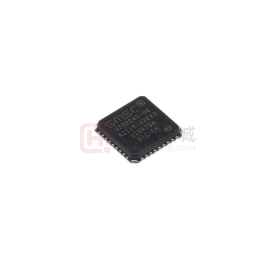
USB224X
Ultra Fast USB 2.0 Multi-Format, SD/MMC, and MS Flash
Media Controllers
Highlights
The Microchip USB224x is a USB 2.0 compliant, HiSpeed bulk only1 mass storage class peripheral controller intended for reading and writing to popular flash
media from the xD-Picture CardTM (xD)2, Memory
Stick® (MS), Secure Digital (SD), and MultiMediaCardTM (MMC) families.
The USB224x is a fully integrated, single chip solution
capable of ultra high performance operation. Average
sustained transfer rates exceeding 35 MB/s are possible if the media and host can support those rates. The
USB2244/44i includes provisions to read/write secure
media formats.
General Features
• Low pin count 36-pin QFN (6x6 mm) RoHS compliant package
• USB2240/40I/41/41I
- Targeted for applications in which single or
"combo" media sockets are used
• Hardware-controlled data flow architecture for all
self-mapped media
• Pipelined hardware support for access to nonself-mapped media
• Order number with “I” denote the products that
support the industrial temperature range of -40ºC
to 85ºC
• Support included for secure media format on a
licensed, customized basis
- USB2244/44I: SD Secure
Hardware Features
• Single chip flash media controller with
- USB2240/40I/41/4I: multiplexed interface for
use with “combo” card sockets
- USB2244/44I: SD/MMC flash media reader/
writer
• MMC Streaming Mode support
• Extended configuration options
- xD player mode operation
- Socket switch polarities, etc.
1.Bulk only is not applicable to USB2240/40i/41/41i.
2.xD-Picture Card is not applicable to USB2241/41i.
2010 - 2015 Microchip Technology Inc.
•
•
•
•
Media Activity LED
On board 24 MHz crystal driver circuit
Optional external 24 MHz clock input3
Internal card power FET
- 200 mA
- "Fold-back" short circuit protection
• 8051 8-bit microprocessor
- 60 MHz - single cycle execution
- 64 KB ROM | 14 KB RAM
• Supports a single external 3.3 V supply source;
internal regulators provide 1.8 V internal core voltage for additional bill of materials and power savings
• Optimized pinout improves signal routing which
eases implementation for improved signal integrity
Flash Media Specification Compliance
• Secure Digital 2.0
- HS-SD, SDHC
- TransFlashTM and reduced form factor media
• MultiMediaCard 4.2
- 1/4/8-bit MMC
• Memory Stick Formats
- MS 1.43, Pro 1.02, Duo 1.10
- Pro-HG Duo 1.01
–MS, MS Duo, HS-MS, MS Pro-HG, MS Pro
• xD-Picture Card 1.2
Software Features
• Customizable vendor specific data
• Optimized for low latency interrupt handling
• Reduced memory footprint
Applications
•
•
•
•
•
Flash media card reader/writers
Desktop and mobile PCs
Printers
Consumer A/V and media players/viewers
Compatible with
–Microsoft® VistaTM and Vista ReadyBoostTM
–Windows® XP, ME, 2K SP4
–Apple Mac OSx®
–Linux Mass Storage Class Drivers
3.Only applicable to USB2240/40i/41/41i.
DS00001979A-page 1
�USB224X
TO OUR VALUED CUSTOMERS
It is our intention to provide our valued customers with the best documentation possible to ensure successful use of your Microchip
products. To this end, we will continue to improve our publications to better suit your needs. Our publications will be refined and
enhanced as new volumes and updates are introduced.
If you have any questions or comments regarding this publication, please contact the Marketing Communications Department via
E-mail at docerrors@microchip.com. We welcome your feedback.
Most Current Data Sheet
To obtain the most up-to-date version of this data sheet, please register at our Worldwide Web site at:
http://www.microchip.com
You can determine the version of a data sheet by examining its literature number found on the bottom outside corner of any page.
The last character of the literature number is the version number, (e.g., DS30000000A is version A of document DS30000000).
Errata
An errata sheet, describing minor operational differences from the data sheet and recommended workarounds, may exist for current devices. As device/documentation issues become known to us, we will publish an errata sheet. The errata will specify the
revision of silicon and revision of document to which it applies.
To determine if an errata sheet exists for a particular device, please check with one of the following:
• Microchip’s Worldwide Web site; http://www.microchip.com
• Your local Microchip sales office (see last page)
When contacting a sales office, please specify which device, revision of silicon and data sheet (include -literature number) you are
using.
Customer Notification System
Register on our web site at www.microchip.com to receive the most current information on all of our products.
DS00001979A-page 2
2010 - 2015 Microchip Technology Inc.
�USB224X
1.0
INTRODUCTION
The Microchip USB224x is a flash media card reader solution fully compliant with the USB 2.0 specification. All required
resistors on the USB ports are integrated into the device. This includes all series termination resistors on D+ and D–
pins and all required pull-down and pull-up resistors. The over-current sense inputs for the downstream facing ports
have internal pull-up resistors.
1.1
Hardware Features
•
•
•
•
Single chip flash media controller in low pin count 36-pin QFN, RoHS compliant package
Commercial temperature products support 0°C to +70°C: USB2240/41 and USB2244
Industrial temperature products support -40°C to +85°C: USB2240I/41I and USB2244I
8051 8-bit microprocessor
- 60 MHz - single cycle execution
- 64 KB ROM |14 KB RAM
• Supports a single external 3.3 V supply source; internal regulators provide 1.8 V internal core voltage for additional bill of materials and power savings
Compliance with the following flash media card specifications:
• Secure Digital 2.0
- HS-SD and SDHC
- TransFlash™ and reduced form factor media
• MultiMediaCard 4.2
- 1/4/8 bit MMC
• Memory Stick 1.43
• Memory Stick Pro Format 1.02
• Memory Stick Pro-HG Duo Format 1.01
- Memory Stick, MS Duo, HS-MS, MS Pro-HG, MS Pro
• Memory Stick Duo 1.10
• xD-Picture Card 1.2
1.2
Software Features
• If the OEM is using an external EEPROM, the following features are available:
- Customizable vendor, product, language, and device ID’s
- 12-hex digits maximum for the serial number string
- 28-character manufacturer ID and product strings for the flash media reader/writer
- LED blink interval or duration
2010 - 2015 Microchip Technology Inc.
DS00001979A-page 3
�USB224X
2.0
ACRONYMS
ATA:
Advanced Technology Attachment
FET:
Field Effect Transistor
LUN:
Logical Unit Number
MMC:
MultiMediaCard
MSC:
Memory Stick Controller1
PLL:
Phase-Locked Loop
QFN:
Quad Flat No leads
RoHS:
Restriction of Hazardous Substances Directive
RXD:
Received eXchange Data
SDC:
Secure Digital Controller
SIE:
Serial Interface Engine
TXD:
Transmit eXchange Data
UART:
Universal Asynchronous Receiver-Transmitter
UCHAR:
Unsigned Character
UINT:
Unsigned Integer
1.Not applicable to USB2244/44i.
DS00001979A-page 4
2010 - 2015 Microchip Technology Inc.
�USB224X
3.0
BLOCK DIAGRAMS
FIGURE 3-1:
USB2240/40I/41/41I BLOCK DIAGRAM
USB2240/40I
USB2241/41I*
USB
Host
SIE
CTL
PHY
AUTO_CBW
PROC
BUS
INTFC
BUS FMDU
INTFC CTL
SD/
MMC
FMI
MS
Multiplexed
Interface
xD*
3.3 V
EP0 TX
EP0 RX
1.8 V Reg
BUS
INTFC
VDD18
RAM
4K
total
EP1 RX
EP1 TX
EP2 RX
EP2 TX
24 MHz
Crystal
PLL
XDATA BRIDGE
+ BUS ARBITER
VDD18PLL
3.3 V
1.8 V Reg
PWR_FET1
RAM
10 KB
ROM
64 KB
ADDR
MAP
Program Memory I/O Bus
SPI
Interface
CRD_PWR
SPI
Interface
Trace FIFO
Clock
Generation and
Control
8051
PROCESSOR
SFR
RAM
NOTE: xD-Picture Card is not applicable to USB2241/41i.
2010 - 2015 Microchip Technology Inc.
DS00001979A-page 5
�USB224X
FIGURE 3-2:
USB2244/44I BLOCK DIAGRAM
USB2244/USB2244I
USB
Host
SIE
CTL
PHY
AUTO_CBW
PROC
BUS
INTFC
BUS FMDU
INTFC CTL
FMI
SD/
MMC
Media
Interface
3.3 V
EP0 TX
EP0 RX
1.8 V Reg
BUS
INTFC
VDD18
RAM
4K
total
EP1 RX
EP1 TX
EP2 RX
EP2 TX
24 MHz
Crystal
PLL
XDATA BRIDGE
+ BUS ARBITER
VDD18PLL
3.3 V
1.8 V Reg
PWR_FET1
RAM
10 KB
ROM
64 KB
ADDR
MAP
Program Memory I/O Bus
CRD_PWR
SPI
Interface
SPI
Interface
Trace FIFO
Clock
Generation and
Control
8051
PROCESSOR
DS00001979A-page 6
SFR
RAM
2010 - 2015 Microchip Technology Inc.
�USB224X
PIN CONFIGURATIONS
RXD / SDA
SD_nCD
xD_D5 / SD_D2
MS_INS
xD_D6 / SD_D3 / MS_D3
VDD33
CRD_PWR
xD_D7 / SD_D4 / MS_D2
(xD_nCD)
26
25
24
23
22
21
20
19
USB2240/USB2240I 36-PIN QFN DIAGRAM
27
FIGURE 4-1:
TEST
28
18
RESET_N
NC
29
17
xD_nB/R
xD_D4 / (SD_WP) / MS_SCLK
30
16
xD_nRE
TXD / SCK / MS_SKT_SEL
31
XTAL2
32
XTAL1 (CLKIN)
33
VDD18PLL
34
RBIAS
35
VDDA33
36
USB2240/2240I
(Top View QFN-36)
1
2
3
4
5
6
7
8
9
LED
USB-
xD_D3 / SD_D1 / MS_D5
xD_D2 / SD_D0 / MS_D4
VDD33
xD_D1 / SD_D7 / MS_D6
xD_D0 / SD_D6 / MS_D7
xD_nWP / SD_CLK / MS_BS
Ground Pad
(must be connected to VSS)
USB+
4.0
15
xD_nCE
14
VDD33
13
VDD18
12
xD_nWE
11
xD_CLE / SD_CMD / MS_D0
10
xD_ALE / SD_D5 / MS_D1
Indicates pins on the bottom of the device.
2010 - 2015 Microchip Technology Inc.
DS00001979A-page 7
�USB224X
NC
VDD33
22
19
SD_D3 / MS_D3
23
CRD_PWR
MS_INS
24
SD_D4 / MS_D2
SD_D2
25
20
SD_nCD
26
21
RXD / SDA
USB2241/USB2241I 36-PIN QFN DIAGRAM
27
FIGURE 4-2:
TEST
28
18
NC
29
17
NC
SD_WP / MS_SCLK
30
16
NC
TXD / SCK / MS_SKT_SEL
31
15
NC
XTAL2
32
XTAL1 (CLKIN)
33
VDD18PLL
34
2
3
4
5
6
7
8
9
USB+
USB-
SD_D1 / MS_D5
SD_D0 / MS_D4
VDD33
SD_D7 / MS_D6
SD_D6 / MS_D7
SD_CLK / MS_BS
36
1
35
Ground Pad
(must be connected to VSS)
LED
RBIAS
VDDA33
USB2241/2241I
(Top View QFN-36)
RESET_N
14
VDD33
13
VDD18
12
NC
11
SD_CMD / MS_D0
10
SD_D5 / MS_D1
Indicates pins on the bottom of the device.
DS00001979A-page 8
2010 - 2015 Microchip Technology Inc.
�USB224X
NC
VDD33
22
19
SD_D3
23
CRD_PWR
NC
24
SD_D4
SD_D2
25
20
SD_nCD
26
21
RXD / SDA
27
USB2244/USB2244I 36-PIN QFN DIAGRAM
TEST
28
18
RESET_N
NC
29
17
NC
SD_WP
30
16
NC
TXD / SCK
31
15
NC
5
6
7
8
9
VDD33
SD_D7
SD_D6
SD_CLK
36
4
VDDA33
SD_D1
35
SD_D0
RBIAS
Ground Pad
(must be connected to VSS)
3
34
USB-
VDD18PLL
2
33
1
32
LED
XTAL2
XTAL1 (CLKIN)
USB2244/2244I
(Top View QFN-36)
USB+
FIGURE 4-3:
14
VDD33
13
VDD18
12
NC
11
SD_CMD
10
SD_D5
Indicates pins on the bottom of the device.
2010 - 2015 Microchip Technology Inc.
DS00001979A-page 9
�USB224X
5.0
PIN TABLES
TABLE 5-1:
USB2240/2240I 36-PIN QFN PACKAGE
xD/SD/MS INTERFACE (18 PINS)
xD_D3 /
SD_D1 /
MS_D5
xD_D2 /
SD_D0 /
MS_D4
xD_D1 /
SD_D7 /
MS_D6
xD_D0 /
SD_D6 /
MS_D7
xD_nWP /
SD_CLK /
MS_BS
xD_ALE /
SD_D5 /
MS_D1
xD_CLE /
SD_CMD /
MS_D0
xD_D7 /
SD_D4 /
MS_D2
xD_D6 /
SD_D3 /
MS_D3
xD_D5 / SD_D2
xD_nRE
xD_nWE
xD_D4 /
SD_WP /
MS_SCLK
xD_nB/R
xD_nCE
MS_INS
xD_nCD
SD_nCD
USB INTERFACE (5 PINS)
USB+
USB-
XTAL1 (CLKIN)
XTAL2
RBIAS
MISC (7 Pins)
LED
RXD /
SDA
NC
CRD_PWR
TEST
RESET_N
TXD /
SCK /
MS_SKT_SEL
DIGITAL, POWER (6 PINS)
(3) VDD33
VDDA33
VDD18
VDD18PLL
TOTAL 36
DS00001979A-page 10
2010 - 2015 Microchip Technology Inc.
�USB224X
TABLE 5-2:
USB2241/2241I 36-PIN QFN PACKAGE
SD/MS INTERFACE (14 PINS)
SD_D1 /
MS_D5
SD_D0 /
MS_D4
SD_D7 /
MS_D6
SD_D6 /
MS_D7
SD_CLK /
MS_BS
SD_D5 /
MS_D1
SD_CMD /
MS_D0
SD_D4 /
MS_D2
SD_D3 /
MS_D3
SD_D2
SD_WP /
MS_SCLK
MS_INS
NC
SD_nCD
USB INTERFACE (5 PINS)
USB+
USB-
XTAL1 (CLKIN)
XTAL2
RBIAS
MISC (11 Pins)
LED
RXD /
SDA
NC
TXD /
SCK /
MS_SKT_SEL
CRD_PWR
TEST
RESET_N
(4) NC
DIGITAL, POWER (6 PINS)
(3) VDD33
VDDA33
VDD18
VDD18PLL
TOTAL 36
2010 - 2015 Microchip Technology Inc.
DS00001979A-page 11
�USB224X
TABLE 5-3:
USB2244/2244I 36-PIN QFN PACKAGE
SD/MMC INTERFACE (12 Pins)
SD_D0
SD_D1
SD_D2
SD_D3
SD_D4
SD_D5
SD_D6
SD_D7
SD_CLK
SD_CMD
SD_WP
SD_nCD
USB INTERFACE (5 PINS)
USB+
USB-
XTAL1 (CLKIN)
XTAL2
RBIAS
MISC (13 PINS)
LED
RXD /
SDA
NC
TXD /
SCK
CRD_PWR
NC
NC
(4) NC
TEST
RESET_N
DIGITAL, POWER (6 PINS)
(3)VDD33
VDDA33
VDD18
VDD18PLL
TOTAL 36
DS00001979A-page 12
2010 - 2015 Microchip Technology Inc.
�USB224X
6.0
PIN DESCRIPTIONS
This section provides a detailed description of each signal. The signals are arranged in functional groups according to
their associated interface. The pin descriptions are applied when using the internal default firmware and can be referenced in Section 7.0, "Pin Configurations," on page 18. Please reference Section 2.0, "Acronyms," on page 4 for a list
of the acronyms used.
The “n” symbol in the signal name indicates that the active, or asserted, state occurs when the signal is at a low voltage
level. When “n” is not present in the signal name, the signal is asserted at the high voltage level.
The terms assertion and negation are used exclusively. This is done to avoid confusion when working with a mixture of
“active low” and “active high” signals. The term assert, or assertion, indicates that a signal is active, independent of
whether that level is represented by a high or low voltage. The term negate, or negation, indicates that a signal is inactive.
USB224x 36-Pin QFN Pin Descriptions
USB2244/44I
Symbol
USB224X 36-PIN QFN PIN DESCRIPTIONS
USB2241/41I
TABLE 6-1:
USB2240/40I
6.1
Buffer
Type
Description
xD-PICTURE CARD (xD) INTERFACE (APPLIES ONLY TO USB2240/USB2240I)
xD_D[7:0]
xD_nWP
20
23
25
30
4
5
7
8
I/O12PD
9
O12PD
xD Data
These bi-directional data signals have weak internal pulldown resistors.
xD Write Protect
This pin is an active low write protect signal for the xD
device and has a weak pull-down resistor that is
permanently enabled.
xD_ALE
10
O12PD
xD Address Strobe
This pin is an active high Address Latch Enable signal for
the xD device and has a weak pull-down resistor that is
permanently enabled.
xD_CLE
11
O12PD
xD Command Strobe
This pin is an active high Command Latch Enable signal
for the xD device and has a weak pull-down resistor that
is permanently enabled.
xD_nRE
16
O12PU
xD Read Enable
This pin is an active low read strobe signal for the xD
device.
When using the internal FET, this pin has a weak internal
pull-up resistor that is tied to the output of the internal
power FET.
If an external FET is used (Internal FET is disabled), then
the internal pull-up is not available (external pull-ups must
be used).
2010 - 2015 Microchip Technology Inc.
DS00001979A-page 13
�USB224X
xD_nWE
12
USB2244/44I
Symbol
USB2241/41I
USB224X 36-PIN QFN PIN DESCRIPTIONS (CONTINUED)
USB2240/40I
TABLE 6-1:
Buffer
Type
O12PU
Description
xD Write Enable
This pin is an active low write strobe signal for the xD
device.
When using the internal FET, this pin has a weak internal
pull-up resistor that is tied to the output of the internal
power FET.
If an external FET is used (Internal FET is disabled), then
the internal pull-up is not available (external pull-ups must
be used).
xD_nB/R
17
IPU
xD Busy or Data Ready
This pin is connected to the BSY/RDY pin of the xD
device.
When using the internal FET, this pin has a weak internal
pull-up resistor that is tied to the output of the internal
power FET.
If an external FET is used (Internal FET is disabled), then
the internal pull-up is not available (external pull-ups must
be used).
xD_nCD
19
I/O12
xD Card Detection
This is designated by the default firmware as the xDPicture card detection pin.
Note: This pin can be left unconnected if the socket is
not used.
xD_nCE
15
O12PU
xD Chip Enable
This pin is the active low chip enable signal to the xD
device.
When using the internal FET, this pin has a weak internal
pull-up resistor that is tied to the output of the internal
power FET.
If an external FET is used (Internal FET is disabled), then
the internal pull-up is not available (external pull-ups must
be used).
MEMORY STICK (MS) INTERFACE
MS_D[7:0]
8
7
4
5
23
20
10
11
I/O12PD
MS System Data In/Out
These pins are the bi-directional data signals for the MS
device. MS_D0, MS_D2, and MS_D3 have weak pulldown resistors.
In serial mode, the most significant bit (MSB) of each byte
is transmitted first by either MSC or MS device on
MS_D0.
In parallel mode, MS_D1 has a pull-down resistor,
otherwise it is disabled.
In 4- or 8-bit parallel mode, there is a weak pull-down
resistor on all MS_D7 - 0 signals.
DS00001979A-page 14
2010 - 2015 Microchip Technology Inc.
�USB224X
MS_BS
USB2244/44I
USB2241/41I
Symbol
USB224X 36-PIN QFN PIN DESCRIPTIONS (CONTINUED)
USB2240/40I
TABLE 6-1:
9
Buffer
Type
O12
Description
MS Bus State
This pin is connected to the bus state (BS) pin of the MS
device. It is used to control the bus states 0, 1, 2 and 3
(BS0, BS1, BS2 and BS3) of the MS device.
MS_SCLK
30
O12
MS System CLK
This pin is an output clock signal to the MS device.
The clock frequency is software configurable.
MS_INS
24
IPU
MS Card Insertion
This is designated by the default firmware as the Memory
Stick card detection pin.
Note: This pin can be left unconnected if the socket is
not used.
SECURE DIGITAL (SD) / MULTIMEDIACARD (MMC) INTERFACE
SD_D[7:0]
SD_CLK
7
8
10
20
23
25
4
5
7
8
10
20
23
25
4
5
I/O12PU
9
9
O12
SD Data
The pins are bi-directional data signals SD_D0 - SD_D7
and have weak pull-up resistors.
SD Clock
This is an output clock signal to SD/MMC device.
The clock frequency is software configurable.
SD_CMD
11
11
I/O12PU
SD Command
This is a bi-directional signal that connects to the CMD
signal of the SD/MMC device and has a weak internal
pull-up resistor.
SD_WP
SD Write Protect Detection
SD_nCD
SD Card Detect
USB INTERFACE
USB+
USBRBIAS
2
3
I/O-U
35
I-R
USB Bus Data
These pins connect to the USB bus data signals.
USB Transceiver Bias
A 12.0 kΩ, ± 1.0% resistor is attached from VSS to this
pin in order to set the transceiver's internal bias currents.
XTAL1 (CLKIN)
33
ICLKx
24 MHz Crystal (External clock input)
This pin can be connected to one terminal of the crystal
or can be connected to an external 24 MHz clock when a
crystal is not used.
XTAL2
32
OCLKx
24 MHz Crystal
This is the other terminal of the crystal, or it is left open
when an external clock source is used to drive
XTAL1(CLKIN).
VDDA33
36
2010 - 2015 Microchip Technology Inc.
3.3 V Analog Power
DS00001979A-page 15
�USB224X
VDD18PLL
USB2244/44I
Symbol
USB2241/41I
USB224X 36-PIN QFN PIN DESCRIPTIONS (CONTINUED)
USB2240/40I
TABLE 6-1:
Buffer
Type
34
Description
1.8 V PLL Power
+1.8 V Filtered analog power for internal PLL. This pin
must have a 1.0 μF ± 20% (ESR < 0.1 Ω) capacitor to
VSS.
MISC
LED
I/O12
LED: Can be used as an LED output.
RXD /
I
RXD: This signal can be used as input to the RXD of
UART in the device. Custom firmware is required to
activate this function.
SDA
I/O12
SDA: This is the data pin when used with an external
serial EEPROM.
O12
TXD: This signal can be used as an output TXD of UART
in the device. Custom firmware is required to activate this
function.
O12
SCK: This is the clock output when used with an external
EEPROM.
I
MS_SKT_SEL: On the positive edge of RESET_N, this
pin is sampled to determined the Memory Stick socket
size.
TXD /
1
31
SCK /
MS_SKT_SEL
1 = 8-bit
0 = 4-bit
CRD_PWR
21
I/O200
CRD_PWR: Card power drive of 3.3 V at either 100 mA
or 200 mA.
RESET_N
18
IS
RESET Input: This active low signal is used by the
system to reset the chip. The active low pulse should be
at least 1 μs wide.
TEST
28
I
TEST Input: Tie this pin to ground for normal operation.
NC
12
15
16
17
VDD18
13
+1.8 V core power. This pin must have a 1.0 μF ± 20%
(ESR