USB2642
USB 2.0 Hub and Flash Media Card Controller Combo
General Description
Features
The USB2642 is a USB 2.0 compliant, hi-speed hub
and card reader combo solution. This fully-integrated,
single chip solution provides USB expansion and flash
media reader/writer integration. The Microchip
USB2642 provides an ultra fast interface between a
USB host and today’s popular flash media formats. The
controller allows read/write capability to flash media
including the following:
• Single-chip USB 2.0 hub controller with 2
exposed hi-speed downstream ports
• The dedicated flash media reader is internally
attached to a 3rd downstream port of the hub as a
USB compound device
• Hub and flash media reader/writer configuration
from a single source:
- Configures internal code using an external
SPI ROM
- Supports execution of external code from SPI
Flash EEPROM
- Supports custom vendor, product, and language ID when using an external EEPROM
• Supports full power management with individual
or ganged power control of each downstream port
• Transaction Translator (TT) in the hub supports
operation of FS and LS peripherals
• Single 24 MHz crystal support
• Control of peripheral I2C devices by USB host.
• Supports internally or externally regulated 1.8 V
core voltage operation
• Supports storage addressability of up to 2TB
• RoHS compliant package
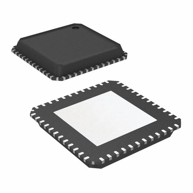
- USB2642: 48-pin (7x7 mm²) QFN
• Temperature ranges:
- Commercial Range (0 ºC to +70 ºC)
- Industrial Range (-40 ºC to +85 ºC)
•
•
•
•
•
Secure DigitalTM (SD)
SD High CapacityTM (SDHC)
SD Extended CapacityTM (SDXC)
MultiMediaCardTM(MMC)
Embedded MultiMediaCardTM (eMMC)
The USB2642 offers a versatile, cost-effective and
energy-efficient hub controller with 2 downstream USB
2.0 ports and a flash media interface. The flash media
interface can support sustained transfer rates exceeding 35 MB/s.
Additionally, the USB2642 provides an I2CTM over USB
bridge and an SD over USB bridge. The I2C bridge
allows for control of any I2C slave device operating at
50KHz serial clock.
Highlights
• PortMap
- Flexible port mapping and port disable
sequencing supports multiple platform
designs
• PortSwap
- Programmable USB differential-pair pin locations eases PCB design by aligning USB signal traces directly to connectors
• PHYBoost
- Programmable USB transceiver drive
strength recovers signal integrity
2014-2021 Microchip Technology Inc.
Target Applications
•
•
•
•
•
•
•
Desktop and mobile PCs
Monitors and televisions
Mobile PC docking
Consumer A/V
Media players/viewers
Printers
Flash media card readers/writers
DS00001578F-page 1
�USB2642
TO OUR VALUED CUSTOMERS
It is our intention to provide our valued customers with the best documentation possible to ensure successful use of your Microchip
products. To this end, we will continue to improve our publications to better suit your needs. Our publications will be refined and
enhanced as new volumes and updates are introduced.
If you have any questions or comments regarding this publication, please contact the Marketing Communications Department via
E-mail at docerrors@microchip.com. We welcome your feedback.
Most Current Data Sheet
To obtain the most up-to-date version of this data sheet, please register at our Worldwide Web site at:
http://www.microchip.com
You can determine the version of a data sheet by examining its literature number found on the bottom outside corner of any page.
The last character of the literature number is the version number, (e.g., DS30000000A is version A of document DS30000000).
Errata
An errata sheet, describing minor operational differences from the data sheet and recommended workarounds, may exist for current devices. As device/documentation issues become known to us, we will publish an errata sheet. The errata will specify the
revision of silicon and revision of document to which it applies.
To determine if an errata sheet exists for a particular device, please check with one of the following:
• Microchip’s Worldwide Web site; http://www.microchip.com
• Your local Microchip sales office (see last page)
When contacting a sales office, please specify which device, revision of silicon and data sheet (include -literature number) you are
using.
Customer Notification System
Register on our web site at www.microchip.com to receive the most current information on all of our products.
DS00001578F-page 2
2014-2021 Microchip Technology Inc.
�USB2642
Table of Contents
1.0 Overview ......................................................................................................................................................................................... 4
2.0 Block Diagram ................................................................................................................................................................................. 6
3.0 USB2642 Pin Configuration ............................................................................................................................................................ 7
4.0 Pin Table ......................................................................................................................................................................................... 8
5.0 Pin Descriptions .............................................................................................................................................................................. 9
6.0 Pin Reset States ........................................................................................................................................................................... 17
7.0 Configuration Options ................................................................................................................................................................... 19
8.0 DC Parameters ............................................................................................................................................................................. 42
9.0 AC Specifications .......................................................................................................................................................................... 46
10.0 Package Outlines ........................................................................................................................................................................ 48
11.0 Revision History .......................................................................................................................................................................... 50
Appendix A: Acronyms ........................................................................................................................................................................ 51
Appendix B: References ..................................................................................................................................................................... 52
The Microchip Web Site ...................................................................................................................................................................... 53
Customer Change Notification Service ............................................................................................................................................... 53
Customer Support ............................................................................................................................................................................... 53
Product Identification System ............................................................................................................................................................. 54
2014-2021 Microchip Technology Inc.
DS00001578F-page 3
�USB2642
1.0
OVERVIEW
1.1
Introduction
The USB2642 offers a USB 2.0 compliant, versatile, cost-effective and energy-efficient hi-speed hub controller with 2
downstream USB ports and an SD/MMC flash media card interface. The dedicated flash media reader is internally
attached to a 3rd downstream port of the hub as a USB compound device. This combo solution supports today’s popular
multi-format flash media card formats. The flash media interface can support sustained transfer rates exceeding 35 MB/
s if the media and host support those rates.
The USB2642 also provides I2C over USB. The I2C bridge allows for control of any I2C device operating at 50kHz clock.
The USB2642 will attach to an upstream port as either a full-speed or full-/hi-speed hub. The hub supports low-speed,
full-speed, and hi-speed (if operating as a full-/hi-speed hub) downstream devices on all of the enabled downstream
ports.
All required resistors on the USB ports are integrated into the hub. This includes all series termination resistors on D+
and D- pins and all required pull-down and pull-up resistors. The over-current sense inputs for the downstream facing
ports have internal pull-up resistors.
The USB2642 includes programmable features such as:
PortMap which provides flexible port mapping and disable sequences. The downstream ports of a USB2642 hub can
be reordered or disabled in any sequence to support multiple platform designs with minimum effort. For any port that is
disabled, the USB2642 automatically reorders the remaining ports to match
the USB host controller’s port numbering scheme.
PortSwap which adds per-port programmability to USB differential-pair pin
locations. PortSwap allows direct alignment of USB signals (D+/D-) to connectors avoiding uneven trace length or crossing of the USB differential signals on the PCB.
PHYBoost which enables four programmable levels of USB signal drive
strength in downstream port transceivers. PHYBoost attempts to restore USB
signal integrity. The diagram on the right shows an example of Hi-Speed USB
eye diagrams before (PHYBoost at 0%) and after (PHYBoost at 12%) signal
integrity restoration in a compromised system environment.
DS00001578F-page 4
2014-2021 Microchip Technology Inc.
�USB2642
1.2
1.2.1
•
•
•
•
•
•
Device Features
HARDWARE FEATURES
Single-chip hub, flash media controller, and I2C device control over USB
Supports commercial (0 °C to +70 °C) and industrial (-40 °C to +85 °C) temperature ranges
Transaction Translator (TT) in the hub supports operation of FS and LS peripherals
Full power management with individual or ganged power control of each downstream port
Optional support for external firmware access via SPI
Code execution via SPI ROM which must meet the following qualifications:
- 60 MHz operation support
- Single bit or dual bit mode support
- Mode 0 or mode 3 SPI support
Compliant with the following flash media card specifications:
• Secure Digital 2.0
- SDSC, SDHC, and SDXC
- microSD and reduced form factor media
- Supports storage addressability of up to 2TB
• MultiMediaCard 4.2
- 1/4/8 bit
- Includes support for eMMC devices
• Control of I2C device using the I2C over USB bridge
• Supports internal regulator for 1.8 V core operation
• Supports external regulator for 1.8 V core operation
1.2.2
CONFIGURABLE FEATURES
Default configuration is loaded by USB2642 following a reset. The USB2642 may also be configured by an external I2C
EEPROM or external SPI ROM flash, where the following features are supported:
•
•
•
•
•
•
•
•
•
•
•
•
•
•
•
Customizable vendor ID, product ID, and device ID
12-hex digits maximum for the serial number string
29-character manufacturer ID and product strings for flash media reader/writer
Compound device support on a port-by-port basis a port is permanently hardwired to a downstream USB peripheral device
Select over-current sensing and port power control on an individual or ganged (all ports together) basis to match
the circuit board component selection
Port power control and over-current detection/delay features
Configure the delay time for filtering the over-current sense inputs
Configure the delay time for turning on downstream port power
Bus- or self-powered selection
Hub port disable of non-removable configurations
Flexible port mapping and disable sequencing supports multiple platform designs
Programmable USB differential-pair pin location selection eases PCB layout by aligning USB signal lines directly
to connectors
Programmable USB signal drive strength improves USB signal integrity using 4 levels of signal drive strength
Indicate the maximum current that the 2-port hub consumes from the USB upstream port
Manage the maximum current required for the hub controller
2014-2021 Microchip Technology Inc.
DS00001578F-page 5
�DS00001578F-page 6
USB Data
OC Sense/
Downstream Pwr Switch
PHY
Port #3
OC
Sense
Switch
Driver
Transaction
Translator
Serial
Interface
Engine
USB Data OC Sense/
Downstream Pwr Switch
PHY
Port #2
OC
Sense
Switch
Driver
Routing & Port Re-Ordering Logic
Repeater
1.8 V Reg
PLL
24 MHz
Crystal
1.8 V
BRIDGE
Port Controller
Controller
Serial
Interface
SIE
CTL
3K
total
BUS
INTFC
ADDR
MAP
EP2
EP2 RX
RX
EP2 TX
RAM
EP0 TX
EP0 RX
ROM
64K
RAM
6K
SFR
RAM
BUS
INTFC
XDATA BRIDGE
+ BUS ARBITER
Program
Memory
I/O Bus
8051
PROCESSOR
FMI
FMDU
CTL
SD/MMC Socket
eMMM IC
SD/
MMC
BUS
INTFC
AUTO_CBW
PROC
GPIOs
PWR_FET0
SPI
I2C
GPO1
(CRD_PWR)
SPI (4 pins)
I2C (2 pins)
FIGURE 2-1:
Upstream
PHY
Upstream USB
3.3 V
Data
2.0
Bus-Power
Detect/VBUS
Pulse
To Upstream
VBUS
USB2642
BLOCK DIAGRAM
USB2642 BLOCK DIAGRAM
2014-2021 Microchip Technology Inc.
�USB2642
USB2642 PIN CONFIGURATION
CRD_PWR
VDD33
SD_D2
SD_D3
NC
SD_D4
SDA
TEST2
TEST1
VDD33 (OTP)
VDD33
35
34
33
32
31
30
29
28
27
26
25
USB2642 48-PIN QFN - TOP VIEW
SCL
FIGURE 3-1:
36
GPO1
37
24
SD_CMD
RESET_N
38
23
SD_D5
VBUS_DET
39
22
REG_EN
TEST0
40
21
SD_CLK
VDDA33
41
20
SD_D6
USBUP_DP
42
19
SD_D7
USBUP_DM
43
18
SD_D0
XTAL2
44
17
SD_D1
XTAL1 (CLKIN)
45
16
VDD33
VDD18PLL
46
15
VDD18
RBIAS
47
14
SD_nCD
VDDA33
48
13
SD_WP
USB2642
12
VDD33
11
SPI_DI
10
SPI_DO/SDA_EP/SPI_SPD_SEL
9
SPI_CLK/SCL_EP
8
SPI_CE_N
7
PRTCTL3
6
PRTCTL2
5
VDDA33
4
USBDN_DP3
2
3
USBDN_DM3
USBDN_DM2
1
e3
USBDN_DP2
3.0
Ground Pad
(must be connected
to VSS)
Indicates pins on the bottom of the device.
2014-2021 Microchip Technology Inc.
DS00001578F-page 7
�USB2642
4.0
PIN TABLE
TABLE 4-1:
USB2642 48-PIN TABLE (GROUPED BY FUNCTION)
Secure Digital (12 pins)
SD_D7
SD_D6
SD_D5
SD_D4
SD_D3
SD_D2
SD_D1
SD_D0
SD_CLK
SD_CMD
SD_nCD
SD_WP
USB 2.0 Interface (10 pins)
USBUP_DP
USBUP_DM
XTAL1 (CLKIN)
XTAL2
RBIAS
(3) VDDA33
VDD18PLL
REG_EN
2-PORT USB Interface (7 pins)
USBDN_DP2
USBDN_DM2
PRTCTL2
PRTCTL3
USBDN_DP3
USBDN_DM3
VBUS_DET
-
SPI Interface (4 pins)
SPI_CE_N
SPI_CLK/
SCL_EP
SPI_DO/
SDA_EP/
SPI_SPD_SEL
SPI_DI
I2C Interface (2 pins)
SCL
SDA
MISC (7 pins)
RESET_N
TEST0
TEST1
GPO1
CRD_PWR
(1) NC
TEST2
POWER (6 pins)
(4) VDD33
VDD33
VDD18
Total 48
DS00001578F-page 8
2014-2021 Microchip Technology Inc.
�USB2642
5.0
PIN DESCRIPTIONS
This section provides a detailed description of each signal. The signals are arranged in functional groups according to
their associated interface. The pin descriptions below are applied when using the internal default firmware and can be
referenced in Section 7.0, Configuration Options. The acronyms used in this chapter can be referenced in Appendix A:
"Acronyms".
An N at the end of a signal name indicates that the active (asserted) state occurs when the signal is at a low voltage
level. When the N is not present, the signal is asserted when it is at a high voltage level. The terms assertion and negation are used exclusively in order to avoid confusion when working with a mixture of active low and active high signals.
The term assert, or assertion, indicates that a signal is active, independent of whether that level is represented by a high
or low voltage. The term negate, or negation, indicates that a signal is inactive.
5.1
USB2642 Pin Description
TABLE 5-1:
Symbol
USB2642 PIN DESCRIPTIONS
48-Pin
QFN
Buffer
Type
Description
Secure Digital Interface
19
20
23
30
32
33
17
18
I/O12PU
SD_CLK
21
O12
SD_CMD
24
I/O12PU
SD_D[7:0]
Secure Digital Data 7-0
These are the bi-directional data signals SD_D0 - SD_D7
Note:
The pull up resistance is a current source that is limited to VDD.
Secure Digital Clock
This is an output clock signal to SD/MMC device.
Secure Digital Command
This is a bi-directional signal that connects to the CMD signal of the SD/
MMC device.
SD_nCD
14
I/O12PU
Secure Digital Card Detect
SD_WP
13
I/O12
Secure Digital Write Protect
I2C Interface
SDA
29
I/O12
Serial Data Signal
SCL
36
I/O12
Serial Clock
USB Interface
USBUP_DM
USBUP_DP
43
42
I/O-U
USBDN_DM
[3:2]
USBDN_DP
[3:2]
3
1
4
2
I/O-U
USB Bus Data
These pins connect to the upstream USB bus data signals (host port or
upstream hub). USBUP_DM and USBUP_DP can be swapped using the
PortSwap feature.
2014-2021 Microchip Technology Inc.
USB Bus Data
These pins connect to the downstream USB bus data signals and can be
swapped using the PortSwap feature.
DS00001578F-page 9
�USB2642
TABLE 5-1:
Symbol
USB2642 PIN DESCRIPTIONS
48-Pin
QFN
PRTCTL[3:2]
7
6
Buffer
Type
Description
I/OD12PU USB Power Enable
As an output, these pins enables power downstream USB peripheral
devices. See Section 5.3, "Port Power Control" for diagram and usage
instructions.
As an input, when the power is enabled, these pins monitor the overcurrent condition. When an over-current condition is detected, these pins
turn the power off.
VBUS_DET
39
I
Detect Upstream VBUS Power
The Microchip hub monitors VBUS_DET to determine when to assert the
internal D+ pull-up resistor (signaling a connect event).
When designing a detachable hub, connect this pin to the VBUS power
pin of the USB port that is upstream of the hub.
For self-powered applications with a permanently attached host, this pin
should be pulled up, typically to VDD33.
VBUS is a 3.3 volt input. A resistor divider must be used when connecting
to 5 volts of USB power.
RBIAS
47
I-R
USB Transceiver Bias
A 12.0 kΩ, ±1.0% resistor is attached from VSS to this pin in order to set
the transceiver's internal bias currents.
XTAL1 (CLKIN)
45
ICLKx
24 MHz Crystal Input/External Clock Input
This pin can be connected to one terminal of the crystal or it can be
connected to an external 24 MHz clock when a crystal is not used.
XTAL2
44
OCLKx
24 MHz Crystal Output
This is the other terminal of the crystal, or a no connect pin, when an
external clock source is used to drive XTAL1 (CLKIN).
VDD18PLL
46
-
1.8 V PLL Power Bypass
This pin is the 1.8 V power bypass for the PLL. This pin requires an
external bypass capacitor of 1.0 µF.
If REG_EN is low, this pin serves as a power supply (1.8 V) for the device.
VDDA33
5
41
48
-
3.3 V Analog Power
• 48QFN - Pin 48 requires an external bypass capacitor of 4.7 µF.
SPI Interface
SPI_CE_N
8
O12
SPI Chip Enable
This is the active low chip enable output. If the SPI interface is enabled,
drive this pin high in power down states.
SPI_CLK/
9
I/O12
SPI Clock
This is the SPI clock out to the serial ROM. See Section 5.4, "ROM Boot
Sequence" for diagram and usage instructions.
During reset, this pin is driven low.
SCL_EP
DS00001578F-page 10
When configured, this is the I²C EEPROM clock pin.
2014-2021 Microchip Technology Inc.
�USB2642
TABLE 5-1:
USB2642 PIN DESCRIPTIONS
Symbol
48-Pin
QFN
Buffer
Type
SPI_DO/
10
I/O12
Description
SPI Data Out
This is the data out for the SPI port. See Section 5.4, "ROM Boot
Sequence" for diagram and usage instructions.
SDA_EP
This pin is the data pin when the device is connected to the optional I²C
EEPROM.
SPI_SPD_SEL
This pin is used to pick the speed of the SPI interface. During RESET_N
assertion, this pin will be tri-stated with the weak pull-down resistor
enabled. When RESET_N is negated, the value on the pin will be
internally latched, and the pin will revert to SPI_DO functionality.
Additionally, the internal pull-down will be disabled.
0 : 30 MHz
1 : 60 MHz
If the latched value is 1, then the pin is tri-stated when the chip is in the
suspend state.
If the latched value is 0, then the pin is driven low during a suspend state.
SPI_DI
11
I/O12PD
SPI Data In
This is the data in to the controller from the SPI ROM.
Misc
GPO1
37
I/O12
This general purpose pin is set to be used as an output.
CRD_PWR
35
I/O200
Card power drive: 3.3 V (200 mA)
This pin powers the multiplexed flash media interface (slot) for the SD/
MMC interface.
Bits 0, 1, 2, and 3 control FET 2 of Register A5h. See Section 7.4.2.11,
"A4h-A5h: LUN 0 Power Configuration," on page 26 for more information.
NC
31
IPU
REG_EN
22
IPU
Regulator Enable
This pin is internally pulled up to enable the internal 1.8 V regulators. In
order to disable the regulators, this pin will need to be externally
connected to ground.
When the internal regulator is enabled, the 1.8 V power pins must be left
unconnected, except for the required bypass capacitors.
RESET_N
38
I
RESET input
This active low signal is used by the system to reset the chip. The active
low pulse should be at least 1 µs wide.
TEST[2:0]
28
27
40
IPD
TEST Input
Tie these test pins to ground for normal operation.
Digital/Power/Ground
VDD18
15
-
1.8 V Digital Core Power Bypass
This pin requires an external bypass capacitor of 1.0 µF.
If REG_EN is low, this pin serves as a power supply (1.8 V) for the device.
VDD33
VDD33 (OTP)
12
16
25
34
-
26
-
3.3 V Power and Regulator Input
• 48QFN - Pin 16 requires an external bypass capacitor of 4.7 µF minimum.
2014-2021 Microchip Technology Inc.
3.3 V Power
DS00001578F-page 11
�USB2642
TABLE 5-1:
USB2642 PIN DESCRIPTIONS
Symbol
48-Pin
QFN
Buffer
Type
VSS
ePad
-
Description
Ground Pad
The ground pad is the only VSS for the device and must be tied to ground
with multiple vias.
5.2
Buffer Type Descriptions
TABLE 5-2:
USB2642 BUFFER TYPE DESCRIPTIONS
Buffer
Description
I
Input
IPU
Input with weak internal pull-up
IS
Input with Schmitt trigger
I/O12
Input/output buffer with 12 mA sink and 12 mA source
I/O200
Input/output buffer 12 mA with FET disabled, 100/200 mA source only when the FET is
enabled
I/O12PD
Input/output buffer with 12 mA sink and 12 mA source, with an internal weak pull-down
resistor
I/O12PU
Open drain, 12 mA sink with pull-up. Input with Schmitt trigger
I/OD12PU
Input/open drain output buffer with a 12 mA sink
O12
Output buffer with a 12 mA sink and a 12 mA source
ICLKx
XTAL clock input
OCLKx
XTAL clock output
I/O-U
Analog input/output defined in USB Specification (Appendix B)
I-R
RBIAS
5.3
Port Power Control
5.3.1
PORT POWER CONTROL USING USB POWER SWITCH
The USB2642 has a single port power control and over-current sense signal for each downstream port. When disabling
port power, the driver will actively drive a 0. To avoid unnecessary power dissipation, the internal pull-up resistor will be
disabled at that time. When port power is enabled, the output driver is disabled, and the pull-up resistor is enabled creating an open drain output.
If there is an over-current situation, the USB Power Switch will assert the open drain OCS signal. The Schmitt trigger
input will detect this event as a low. The open drain output does not interfere. The over-current sense filter handles the
transient conditions, such as low voltage, while the device is powering up.
DS00001578F-page 12
2014-2021 Microchip Technology Inc.
�USB2642
FIGURE 5-1:
PORT POWER CONTROL WITH USB POWER SWITCH
5V
PRTCTL3
OCS
USB Power
Switch
EN
USB
Device
USB2642
5V
PRTCTL2
OCS
USB Power
Switch
EN
USB
Device
5.3.2
PORT POWER CONTROL USING A POLY FUSE
When using the USB2642 with a poly fuse, an external diode must be used (see Figure 5-2). When disabling port power,
the USB2642 driver will drive a 0. This procedure will have no effect since the external diode will isolate the pin from the
load. When port power is enabled, the USB2642 output driver is disabled, and the pull-up resistor is enabled which creates an open drain output. This means that the pull-up resistor is providing 3.3 volts to the anode of the diode. If there
is an over-current situation, the poly fuse will open. This will cause the cathode of the diode to go to zero volts. The
anode of the diode will be at 0.7 volts, and the Schmitt trigger input will register this as a low resulting in an over-current
detection. The open drain output does not interfere.
2014-2021 Microchip Technology Inc.
DS00001578F-page 13
�USB2642
FIGURE 5-2:
PORT POWER CONTROL WITH SINGLE POLY FUSE AND MULTIPLE LOADS
5V
PRTCTL3
USB
Device
USB2642
5V
PRTCTL2
USB
Device
When using a single poly fuse to power all devices, note that for the ganged situation, all power control pins must be
tied together.
DS00001578F-page 14
2014-2021 Microchip Technology Inc.
�USB2642
FIGURE 5-3:
PORT POWER WITH GANGED CONTROL WITH POLY FUSE
5V
PRTCTL3
Poly Fuse
USB2642
PRTCTL2
5.4
USB
Device
USB
Device
ROM Boot Sequence
After power-on reset, the internal firmware checks for an external SPI flash device that contains a valid signature of
2DFU (device firmware upgrade) beginning at address 0xFFFA. If a valid signature is found, then the external ROM is
enabled and code execution begins at address 0x0000 in the external SPI device. Otherwise, code execution continues
from the internal ROM.
The SPI ROM required for the USB2642 is a recommended minimum of 1 Mbit and support 60 MHz. The frequency
used is set using the SPI_SPD_SEL. For 60 MHz operation, this pin must pulled up through a 100 kΩ resistor. SPI_SPD_SEL is used to choose the speed of the SPI interface. During RESET_N assertion, this pin will be tri-stated with the
weak pull-down resistor enabled. When RESET_N is negated, the value on the pin will be internally latched, and the pin
will revert to SPI_DO functionality, and the internal pull-down is disabled.
The firmware can determine the speed of operation on the SPI port by checking the SPI_SPEED in the SPI_CTL Register
(0x2400 - RESET = 0x02). Both 1- and 2-bit SPI operation is supported. For optimum throughput, a 2-bit SPI ROM is
recommended. Both mode 0 and mode 3 SPI ROMS are also supported.
2014-2021 Microchip Technology Inc.
DS00001578F-page 15
�USB2642
FIGURE 5-4:
SPI ROM CONNECTION
SPI_CE_N
SPI_CLK / SCL_EP
CE#
CLK
USB2642
SPI ROM
SPI_DO / SDA_EP / SPI_SPD_SEL
SPI_DI
DS00001578F-page 16
SI
SO
2014-2021 Microchip Technology Inc.
�USB2642
6.0
PIN RESET STATES
TABLE 6-1:
LEGEND FOR PIN RESET STATES
Symbol
Description
0
Output driven low
1
Output driven high
IP
Input enabled
PU
Hardware enables pull-up
PD
Hardware enables pull-down
none
Hardware disables pad
-
Hardware disables function
Z
Hardware disables pad. Both output driver and input buffers are disabled.
6.1
Pin Reset States
TABLE 6-2:
USB2642 RESET STATES
Reset State
Pin
Pin Name
Function
Input/
Output
PU/
PD
1
USBDN_DM2
USBDN_DM2
IP
PD
2
USBDN_DP2
USBDN_DP2
IP
PD
3
USBDN_DM3
USBDN_DM3
IP
PD
4
USBDN_DP3
USBDN_DP3
IP
PD
6
PRTCTL2
PRTCTL
0
-
7
PRTCTL3
PRTCTL
0
-
8
SPI_CE_N
SPI_CE_N
1
-
9
SPI_CLK/SCL_EP
IO
0
-
10
SPI_DO/SDA_EP/SPI_SPD_SEL
IO
0
PD
11
SPI_DI
SPI_DI
IP
PD
13
SD_WP
IO
0
-
14
SD_nCD
IO
IP
PU
17
SD_D1
none
Z
-
2014-2021 Microchip Technology Inc.
DS00001578F-page 17
�USB2642
TABLE 6-2:
USB2642 RESET STATES (CONTINUED)
Reset State
Pin
Pin Name
Function
Input/
Output
PU/
PD
18
SD_D0
none
Z
-
19
SD_D7
none
Z
-
20
SD_D6
none
Z
-
21
SD_CLK
none
Z
-
22
REG_EN
none
IP
PU
23
SD_D5
none
Z
-
24
SD_CMD
none
Z
-
27
TEST1
none
Z
-
28
TEST2
none
Z
-
29
SDA
IO
IP
PU
30
SD_D4
none
Z
-
31
NC
GPIO
IP
PU
32
SD_D3
none
Z
-
33
SD_D2
none
Z
-
35
CRD_PWR
IO
Z
-
36
SCL
IO
0
-
37
GPO1
GPO
0
-
38
RESET_N
RESET_N
IP
-
39
VBUS_DET
VBUS_DET
IP
-
40
TEST0
TEST
IP
PD
42
USBUP_DP
USBUP_DP
Z
-
43
USBUP_DM
USBUP_DM
Z
-
DS00001578F-page 18
2014-2021 Microchip Technology Inc.
�USB2642
7.0
CONFIGURATION OPTIONS
7.1
Hub
Microchip’s USB2642 hub is fully compliant with the Universal Serial Bus 2.0 Specification (References). See
Chapter 11 (Hub Specification) for general details regarding hub operation and functionality.
The hub provides a single Transaction Translator (TT) shared by both downstream ports. The TT contains 4 non-periodic buffers.
7.1.1
HUB CONFIGURATION OPTIONS
The Microchip hub supports a large number of configurable features (some are mutually exclusive). There are two principal ways to configure the hub:
• default settings
• settings loaded from an external EEPROM or SPI Flash device
7.1.1.1
Power Switching Polarity
The hub will only support active high power controllers.
7.1.2
VBUS DETECT
According to Section 7.2.1 of the USB 2.0 Specification, a downstream port can never provide power to its D+ or D- pullup resistors unless the upstream port’s VBUS is in the asserted (powered) state. The VBUS_DET pin on the hub monitors the state of the upstream VBUS signal and will not pull-up the D+ resistor if VBUS is not active. If VBUS goes from
an active to an inactive state (not powered), the hub will remove power from the D+ pull-up resistor within 10 seconds.
7.2
Card Reader
The Microchip USB2642 is fully compliant with the following flash media card reader specifications:
• Secure Digital 2.0
- SDSC, SDHC, and SDXC
- mircoSD and reduced form factor media
- Supports storage addressability of up to 2TB
• MultiMediaCard 4.2
- 1/4/8 bit
- includes support for eMMC devices
7.3
I2C over USB Bridge
USB2642 offers a I2C over USB bridge functionality. Host initiated SCSI pass-through commands are sent to USB2642
using Mass Storage Class driver to control I2C master interface. Additional support for detecting clock stretching during
reads is also provided.
The following features are exposed through host side I2C API:
• Write_I2C_Stream
Send any length of data over the I2C interface.
The sequence follows the I2C protocol for writing data.
• WriteRead_I2C_Stream
Read any length of data over the I2C interface.
The sequence follows the I2C protocol for reading data.
• GPIO_1_SET_OUTPUT
This method allows an application to assert GPO1 pin. This can be driving RST of the I2C slave device.
For additional configuration information and protocol details, see “USB2642 I2C Over USB Bridge User’s Guide
2014-2021 Microchip Technology Inc.
DS00001578F-page 19
�USB2642
7.4
7.4.1
System Configurations
EEPROM/SPI INTERFACE
The USB2642 can be configured via a 2-wire (I2C) EEPROM (512x8) or an external SPI flash device containing the
firmware for the USB2642. If an external configuration device does not exist the internal default values will be used. If
one of the external devices is used for configuration, the OEM can update the values through the USB interface. The
hub will then attach to the upstream USB host.
The USBDM tool set is available in the Hub Card reader combo software release package.
7.4.2
EEPROM DATA DESCRIPTOR
TABLE 7-1:
INTERNAL FLASH MEDIA CONTROLLER CONFIGURATIONS
Address
Register Name
Description
Internal Default Value
00h-19h
USB_SER_NUM
USB Serial Number
000008264001
(Unicode)
1Ah-1Bh
USB_VID
USB Card Reader
Vendor ID
0424
1Ch-1Dh
USB_PID
USB Card Reader
Product ID
4041
1Eh-21h
USB_LANG_ID
USB Language Identifier
0409
(see Note 1)
22h-5Dh
USB_MFR_STR
USB Manufacturer String
Generic
(Unicode)
5Eh-99h
USB_PRD_STR
USB Product String
Ultra Fast Media Reader
(Unicode)
9Ah
USB_BM_ATT
USB BmAttribute
80h
9Bh
USB_MAX_PWR
USB Max Power
30h (96 mA)
9Ch
ATT_LB
Attribute Lo byte
40h (Reverse SD_WP only)
9Dh
ATT_HLB
Attribute Hi Lo byte
80h (Reverse SD2_WP only)
9Eh
ATT_LHB
Attribute Lo Hi byte
00h
9Fh
ATT_HB
Attribute Hi byte
00h
A0h-A3h
rsvd
A4h
LUN_PWR_LB
LUN Power Lo byte
00h
A5h
LUN_PWR_HB
LUN Power Hi byte
0Ah
A6h-BEh
rsvd
BFh-C5h
DEV3_ID_STR
Device 3 Identifier String
SD/MMC
C6h-CDh
INQ_VEN_STR
Inquiry Vendor String
Generic
CEh-D2h
INQ_PRD_STR
48QFN Inquiry Product
String
2642
D3h
DYN_NUM_LUN
Dynamic Number of LUNs
01h
D4h-D7h
LUN_DEV_MAP
LUN to Device Mapping
FFh, 00h, 00h, 00h
D8h-DAh
rsvd
DS00001578F-page 20
2014-2021 Microchip Technology Inc.
�USB2642
TABLE 7-1:
INTERNAL FLASH MEDIA CONTROLLER CONFIGURATIONS (CONTINUED)
Address
Register Name
Description
Internal Default Value
DBh-DDh
SD_MMC_BUS_TIMING
SD/MMC Bus Timing
Control
59h, 56h, 97h
(Note 2)
Refer to Table 7-2, “Hub Controller Configurations,” on page 22
for a continuation of the register values DEh-17Fh.
Internal Flash Media Controller Extended Configurations:
The registers below are enabled by setting bit 7 of bmAttribute.
100h-106h
CLUN0_ID_STR
LUN 0 Identifier String
COMBO
107h-10Dh
CLUN1_ID_STR
LUN 1 Identifier String
COMBO
10Eh-114h
CLUN2_ID_STR
LUN 2 Identifier String
COMBO
115h-11Bh
CLUN3_ID_STR
LUN 3 Identifier String
COMBO
11Ch-122h
CLUN4_ID_STR
LUN 4 Identifier String
COMBO
123h-129h
rsvd
12Ah-145h
rsvd
146h
DYN_NUM_ EXT_LUN
Dynamic Number of
Extended LUNs
00h
147h-14Bh
LUN_DEV_MAP
LUN to Device Mapping
FFh, FFh, FFh, FFh, FFh
14Ch-17Bh
rsvd
17Ch-17Fh
NVSTORE_SIG2
Non-Volatile Storage
Signature
ecf1
Note that the following applies to the system values and descriptions:
• rsvd = reserved for internal use; do not write to these registers
Note 1: Refer to the USB 2.0 Specification (References) for other language codes.
2: This register value must not be changed from the default value.
2014-2021 Microchip Technology Inc.
DS00001578F-page 21
�USB2642
TABLE 7-2:
HUB CONTROLLER CONFIGURATIONS
Address
Register Name
Description
Internal Default Value
DEh
VID_LSB
Vendor ID Least Significant Byte
24h
DFh
VID_MSB
Vendor ID Most Significant Byte
04h
E0h
PID_LSB
48QFN Product ID Least
Significant Byte
40h
E1h
PID_MSB
Product ID Most Significant Byte
26h
E2h
DID_LSB
Device ID Least Significant Byte
A2h
E3h
DID_MSB
Device ID Most Significant Byte
08h
E4h
CFG_DAT_BYT1
Configuration Data Byte 1
8Bh
E5h
CFG_DAT_BYT2
Configuration Data Byte 2
28h
E6h
CFG_DAT_BYT3
Configuration Data Byte 3
00h
E7h
NR_DEVICE
Non-Removable Devices
02h
E8h
PORT_DIS_SP
Port Disable (Self)
00h
E9h
PORT_DIS_BP
Port Disable (Bus)
00h
EAh
MAX_PWR_SP
Max Power (Self)
01h
EBh
MAX_PWR_BP
Max Power (Bus)
32h
ECh
HC_MAX_C_SP
Hub Controller Max Current (Self)
01h
EDh
HC_MAX_C_BP
Hub Controller Max Current (Bus)
32h
EEh
PWR_ON_TIME
Power-on Time
32h
EFh
BOOST_UP
Boost_Up
00h
F0h
BOOST_3:2
Boost_3:2
00h
F1h
PRT_SWP
PortSwap
00h
F2h
PRTM12
PortMap 12
00h
F3h
PRTM3
PortMap 3
00h
TABLE 7-3:
OTHER INTERNAL CONFIGURATIONS
Address
Register Name
Description
Internal Default Value
F4h
SD_CLK_LIM
SD Clock Limit for the Flash
Media Controller
00h
F5h
rsvd
F6h
MEDIA_SETTINGS
SD1 Timeout Configuration
00h
F7h-FBh
rsvd
FCh-FFh
NVSTORE_SIG
Non-Volatile Storage Signature
ATA2
DS00001578F-page 22
2014-2021 Microchip Technology Inc.
�USB2642
7.4.2.1
00h-19h: USB Serial Number Option
Byte
Name
25:0
USB_SER_NUM
7.4.2.2
Name
1:0
USB_VID
Name
1:0
USB_PID
Name
3:0
USB_LANG_ID
Description
This ID is unique for every product, where the product ID is assigned by the
vendor.
Description
English language code = 0409
22h-5Dh: USB Manufacturer String Length
Byte
Name
59:0
USB_MFR_STR
7.4.2.6
This ID is unique for every vendor, where the vendor ID is assigned by the
USB Implementer’s Forum.
1Eh-21h: USB Language Identifier Option
Byte
7.4.2.5
Description
1Ch-1Dh: USB Product Identifier Option
Byte
7.4.2.4
Maximum string length is 12 hex digits. Must be unique to each device.
1Ah-1Bh: USB Vendor Identifier Option
Byte
7.4.2.3
Description
Description
Maximum string length is 29 characters.
5Eh-99h: USB Product String Length
Byte
Name
59:0
USB_PRD_STR
2014-2021 Microchip Technology Inc.
Description
This string is used during the USB enumeration process by Windows®. The
maximum string length is 29 characters.
DS00001578F-page 23
�USB2642
7.4.2.7
9Ah: USB BmAttribute (1 byte)
Bit
Name
Description
7:0
USB_BM_ATT
Self- or Bus-Power: Selects between self- and bus-powered operation.
The hub is either self-powered (draws less than 2 mA of upstream bus power)
or bus-powered (limited to a 100 mA maximum of upstream power prior to
being configured by the host controller).
When configured as a bus-powered device, the Microchip hub consumes less
than 100 mA of current prior to being configured. After configuration, the buspowered Microchip hub (along with all associated hub circuitry, any embedded devices if part of a compound device, and 100 mA per externally available downstream port) must consume no more than 500 mA of upstream
VBUS current. The current consumption is system dependent, and the OEM
must ensure that the USB 2.0 specifications are not violated.
When configured as a self-powered device,


 工商网监
湘ICP备2023018690号
工商网监
湘ICP备2023018690号
