USBF4100
USB Firmware Memory
Features
• Firmware Memory Companion for the USB491X
Family of USB Controllers
• Targeted for USB 2.0 High-Speed Infotainment
Applications Including:
- Integration with head unit systems
- First, second, and third row USB media hubs
• Memory Size:
- 512 KByte (4 Mbit)
• Single Voltage Read and Write Operations:
- 2.7-3.6V
• Serial Interface Architecture:
- SPI Compatible: Mode 0 and Mode 3
• High Speed Clock Frequency:
- 40 MHz
• READ Support:
- Fast-Read Dual-Output
- Fast-Read Single I/O
• Superior Reliability:
- Endurance: 100,000 Cycles
- Greater than 20 years Data Retention
• Ultra-Low Power Consumption:
- Active Read Current: 5 mA (typical)
- Standby Current: 5 µA (typical)
- Power-down Mode Standby Current: 3 µA (typical)
• Flexible Erase Capability:
- Uniform 4 KByte sectors
- Uniform 64 KByte overlay blocks
• Page Program Mode:
- 256 Bytes/Page
• Fast Erase and Page-Program:
- Chip Erase Time: 250 ms (typical)
- Sector Erase Time: 40 ms (typical)
- Block Erase Time: 80 ms (typical)
- Page-Program Time: 4 ms/ 256 bytes (typical)
• End-of-Write Detection:
- Software polling the BUSY bit in Status Register
• Hold Pin (HOLD#):
- Suspend a serial sequence without deselecting
the device
• Write Protection (WP#):
- Enables/Disables the Lock-Down function of the
status register
2018-2020 Microchip Technology Inc.
• Software Write Protection:
- Write protection through Block-Protection bits in
status register
• Temperature Range:
- Automotive Grade 1: -40°C to 125°C
- Automotive Grade 2: -40°C to 105°C
- Automotive Grade 3: -40°C to 85°C
• Packages Available:
- 8-lead SOIC (150 mils)
- 8-contact USON (2x3 mm)
• All Devices are RoHS Compliant
Product Description
USBF4100, a USB Firmware memory chip, is a companion to the Microchip Automotive USB Smart Hub
devices: USB491X. Factory pre-programming is available for custom firmware and configurations. The
USBF4100 memory function assures proper functionality, providing for decreased development time and
engineering resource, and overall faster time to market.
The USB Firmware memory family features a four-wire,
SPI-compatible interface that allows for a low pin count
package, which occupies less board space and ultimately lowers total system costs. It is manufactured
with proprietary, high-performance CMOS SuperFlash
technology. The split-gate cell design and thick-oxide
tunneling injector attain better reliability and manufacturability compared with alternate approaches ideal for
applications requiring high quality and reliability.
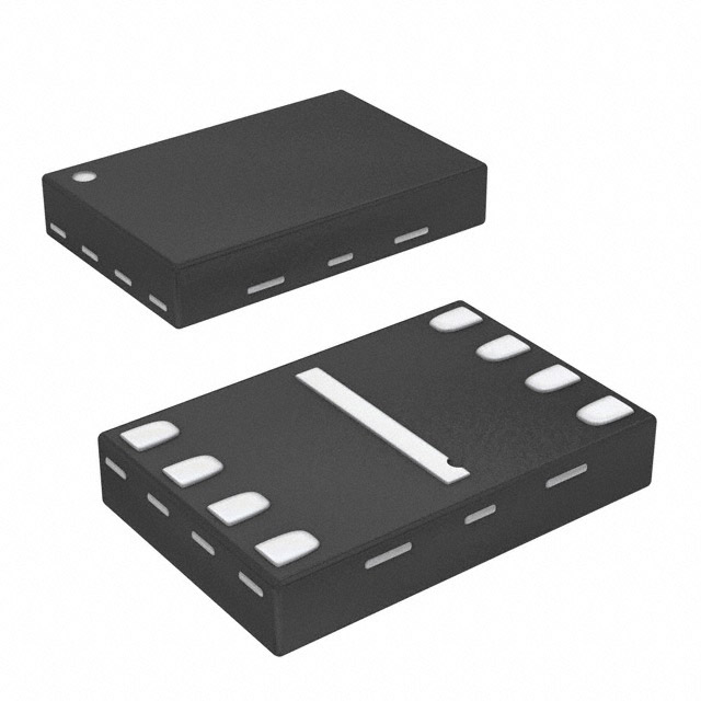
USBF4100 is offered in 8-lead SOIC and 8-contact
USON. See Figure 1-1 for the pin assignments.
DS20005794B-page 1
�USBF4100
TO OUR VALUED CUSTOMERS
It is our intention to provide our valued customers with the best documentation possible to ensure successful use of your Microchip
products. To this end, we will continue to improve our publications to better suit your needs. Our publications will be refined and
enhanced as new volumes and updates are introduced.
If you have any questions or comments regarding this publication, please contact the Marketing Communications Department via
E-mail at docerrors@microchip.com. We welcome your feedback.
Most Current Data Sheet
To obtain the most up-to-date version of this data sheet, please register at our Worldwide Website at:
http://www.microchip.com
You can determine the version of a data sheet by examining its literature number found on the bottom outside corner of any page.
The last character of the literature number is the version number, (e.g., DS30000000A is version A of document DS30000000).
Errata
An errata sheet, describing minor operational differences from the data sheet and recommended workarounds, may exist for current
devices. As device/documentation issues become known to us, we will publish an errata sheet. The errata will specify the revision
of silicon and revision of document to which it applies.
To determine if an errata sheet exists for a particular device, please check with one of the following:
• Microchip’s Worldwide Website; http://www.microchip.com
• Your local Microchip sales office (see last page)
When contacting a sales office, please specify which device, revision of silicon and data sheet (include literature number) you are
using.
Customer Notification System
Register on our website at www.microchip.com to receive the most current information on all of our products.
2018-2020 Microchip Technology Inc.
DS20005794B-page 2
�USBF4100
1.0
PIN ASSIGNMENTS
FIGURE 1-1:
PIN ASSIGNMENTS
CE#
1
8
VDD
SO/SIO1
2
7
HOLD#
WP#
3
6
SCLK
VSS
4
5
SI/SIO0
08-soic-P0.0
8-Lead SOIC
CE#
1
SO/SIO1
2
Top View
8
VDD
7
HOLD#
WP#
3
6
SCK
VSS
4
5
SI/SIO0
25164 08-uson Q3A P1.0
8-Contact USON
TABLE 1-1:
PIN DESCRIPTION
Symbol
Pin Name
Functions
SCK
Serial Clock
To provide the input/output timing of the serial interface.
Commands, addresses, or input data are latched on the rising edge of the clock
input, while output data is shifted out on the falling edge of the clock input.
SI
Serial Data Input
To transfer commands, addresses, or data serially into the device.
Inputs are latched on the rising edge of the serial clock.
SO
Serial Data Output
To transfer data serially out of the device.
Data is shifted out on the falling edge of the serial clock.
SIO[0:1]
Serial Data Input/
To transfer commands, addresses, or data serially into the device, or data out of
Output for Dual I/O the device. Inputs are latched on the rising edge of the serial clock. Data is
Mode
shifted out on the falling edge of the serial clock. These pins are used in Dual
I/O mode
CE#
Chip Enable
The device is enabled by a high to low transition on CE#. CE# must remain low
for the duration of any command sequence. The device is deselected and
placed in Standby mode when CE# is high.
WP#
Write-Protect
The Write-Protect (WP#) pin is used to enable/disable BPL bit in the STATUS
register.
HOLD#
Hold
To temporarily stop serial communication with USB Firmware memory while
device is selected.
VDD
Power Supply
To provide power supply voltage: 2.7-3.6V
VSS
Ground
2018-2020 Microchip Technology Inc.
DS20005794B-page 3
�USBF4100
2.0
DEVICE OPERATION
The USBF4100 supports both Mode 0 (0,0) and Mode
3 (1,1) of SPI bus operations. The difference between
the two modes, as shown in Figure 2-1, is the state of
the SCK signal when the bus master is in Standby
mode and no data is being transferred. The SCK signal
is low for Mode 0 and SCK signal is high for Mode 3.
For both modes, the Serial Data In (SI) is sampled at
the rising edge of the SCK clock signal and the Serial
Data Output (SO) is driven after the falling edge of the
SCK clock signal.
USBF4100 is accessed through the SPI (Serial Peripheral Interface) bus compatible protocol. The SPI bus
consist of four control lines: Chip Enable (CE#) is used
to select the device, and data is accessed through the
Serial Data Input (SI), Serial Data Output (SO), and
Serial Clock (SCK).
FIGURE 2-1:
SPI PROTOCOL
CE#
SCK
SI
MODE 3
MODE 3
MODE 0
MODE 0
Bit 7 Bit 6 Bit 5 Bit 4 Bit 3 Bit 2 Bit 1 Bit 0
MSB
SO
HIGH IMPEDANCE
DON'T CARE
Bit 7 Bit 6 Bit 5 Bit 4 Bit 3 Bit 2 Bit 1 Bit 0
MSB
2018-2020 Microchip Technology Inc.
20005397 F03.0
DS20005794B-page 4
�USBF4100
3.0
INSTRUCTIONS
Instructions are used to read, write (Erase and Program), and configure the USBF4100 devices. The
instruction bus cycles are 8 bits each for commands
(Op Code), data, and addresses. The Write-Enable
(WREN) instruction must be executed prior to Sector
Erase, Block Erase, Page-Program, Write-Status-Register, or Chip Erase instructions. The complete instructions are provided in Table 3-1. All instructions are
synchronized off a high-to-low transition of CE#. Inputs
will be accepted on the rising edge of SCK starting with
TABLE 3-1:
the Most Significant bit. CE# must be driven low before
an instruction is entered and must be driven high after
the last bit of the instruction has been shifted in (except
for Read, Read-ID, and Read-Status-Register instructions). Any low-to-high transition on CE#, before receiving the last bit of an instruction bus cycle, will terminate
the instruction in progress and return the device to
Standby mode. Instruction commands (Op Code),
addresses, and data are all input from the Most Significant bit (MSB) first.
DEVICE OPERATION INSTRUCTIONS
Instruction
Description
Op Code Cycle1
Address Dummy
Data
Maximum
Cycle(s)2 Cycle(s) Cycle(s) Frequency
Read
Read Memory
0000 0011b (03H)
3
0
1 to
High-Speed Read
Read Memory at Higher
Speed
0000 1011b (0BH)
3
1
1 to
Fast-Read DualOutput
Read Memory with Dual Output
0011 1011b (3BH)
3
13
1 to 3
1011 1011b (BBH)
33
13
1 to 3
4 KByte Sector
Erase4
Erase 4 KByte of memory array 0010 0000b (20H)
1101 0111b (D7H)
3
0
0
64 KByte Block
Erase5
Erase 64 KByte block
of memory array
1101 1000b (D8H)
3
0
0
Chip Erase
Erase Full Memory Array
0110 0000b (60H)
or
1100 0111b (C7H)
0
0
0
0000 0010b (02H)
3
Fast-Read Dual I/O Read Memory with Dual
Address Input and Data Output
Page-Program
RDSR
6
WRSR
To program up to 256 Bytes
40 MHz
0
1 to 256
Read-Status-Register
0000 0101b (05H)
0
0
1 to
Write-Status-Register
0000 0001b (01H)
0
0
1
WREN
Write-Enable
0000 0110b (06H)
0
0
0
WRDI
Write-Disable
0000 0100b (04H)
0
0
0
Read-ID
1010 1011b (ABH)
3
0
1 to
JEDEC-ID
JEDEC ID Read
1001 1111b (9FH)
0
0
4 to
DPD
Deep Power-Down Mode
1011 1001b (B9H)
0
0
0
Release from Deep PowerDown or Read ID
1010 1011b (ABH)
0
0
0
RDID7, 8
RDPD8
25 MHz
1.
2.
3.
4.
5.
6.
7.
One bus cycle is eight clock periods.
Address bits above the Most Significant bit of each density can be VIL or VIH.
One bus cycle is four clock periods in Dual Operation
4 KByte Sector Erase addresses: use AMS-A12, remaining addresses are don’t care but must be set either at VIL or VIH.
64 KByte Block Erase addresses: use AMS-A16, remaining addresses are don’t care but must be set either at VIL or VIH.
The Read-Status-Register is continuous with ongoing clock cycles until terminated by a low to high transition on CE#.
Device ID = 6EH is read after three dummy address bytes. The Device ID output stream is continuous until terminated by a
low-to-high transition on CE#.
8. The instructions Release from Deep Power-Down and Read-ID are similar instructions (ABH). Executing Read-ID requires
the ABH instruction, followed by 24 dummy address bits to retrieve the Device ID. Release from Deep Power-Down only
requires the instruction ABH. JEDEC-ID data = 62H 06H 13H 00H.
2018-2020 Microchip Technology Inc.
DS20005794B-page 5
�USBF4100
4.0
ELECTRICAL SPECIFICATIONS
Absolute Maximum Stress Ratings (Applied conditions greater than those listed under “Absolute Maximum Stress Ratings” may cause permanent damage to the device. This is a stress rating only and functional operation of the device at these conditions or conditions greater than those defined in the operational
sections of this data sheet is not implied. Exposure to absolute maximum stress rating conditions may
affect device reliability.)
Temperature Under Bias . . . . . . . . . . . . . . . . . . . . . . . . . . . . . . . . . . . . . . . . . . . . . . . . . -55°C to +125°C
Storage Temperature . . . . . . . . . . . . . . . . . . . . . . . . . . . . . . . . . . . . . . . . . . . . . . . . . . . . -55°C to +150°C
D. C. Voltage on Any Pin to Ground Potential . . . . . . . . . . . . . . . . . . . . . . . . . . . . . . . . -0.5V to VDD+0.5V
Transient Voltage (


 工商网监
湘ICP备2023018690号
工商网监
湘ICP备2023018690号
