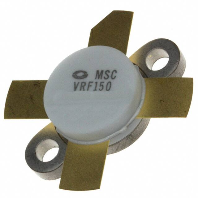
VRF141
VRF141MP
28V, 150W, 175MHz
RF POWER VERTICAL MOSFET
The VRF141 is a gold-metallized silicon n-channel RF power transistor designed for broadband commercial and military applications requiring high power
and gain without compromising reliability, ruggedness, or inter-modulation
distortion.
FEATURES
• Improved Ruggedness V(BR)DSS = 80 V
• 30:1 Load VSWR Capability at Specified Operating Conditions
• 150W with 22dB Typical Gain @ 30MHz, 28V
• Nitride Passivated
• 150W with 13dB Typical Gain @ 175MHz, 28V
• Refractory Gold Metallization
• Excellent Stability & Low IMD
• High Voltage Replacement for MRF141
• Common Source Configuration
• RoHS Compliant
• Available in Matched Pairs
Maximum Ratings
Symbol
VDSS
ID
All Ratings: TC =25°C unless otherwise specified
Parameter
Drain-Source Voltage
VRF141(MP)
Unit
80
V
Continuous Drain Current @ TC = 25°C
20
A
VGS
Gate-Source Voltage
±40
V
PD
Total Device dissipation @ TC = 25°C
300
W
TSTG
TJ
Storage Temperature Range
-65 to 150
Operating Junction Temperature
°C
200
Static Electrical Characteristics
Symbol
Parameter
V(BR)DSS
Drain-Source Breakdown Voltage (VGS = 0V, ID = 100mA)
Min
VDS(ON)
On State Drain Voltage (ID(ON) = 10A, VGS = 10V)
Typ
Max
0.9
1.0
80
Unit
V
IDSS
Zero Gate Voltage Drain Current (VDS = 60V, VGS = 0V)
1.0
mA
IGSS
Gate-Source Leakage Current (VDS = ±20V, VDS = 0V)
1.0
μA
gfs
Forward Transconductance (VDS = 10V, ID = 5A)
5.0
VGS(TH)
Gate Threshold Voltage (VDS = 10V, ID = 100mA)
2.9
3.6
4.4
V
Min
Typ
Max
Unit
0.60
°C/W
Max
Unit
mhos
Thermal Characteristics
Symbol
RθJC
Characteristic
Junction to Case Thermal Resistance
Symbol
Parameter
Test Conditions
Min
Typ
CISS
Input Capacitance
VGS = 0V
400
Coss
Output Capacitance
VDS = 28V
375
Crss
Reverse Transfer Capacitance
f = 1MHz
50
CAUTION: These Devices are Sensitive to Electrostatic Discharge. Proper Handling Procedures Should Be Followed.
Microsemi Website - http://www.microsemi.com
pF
050-4942 Rev D 9-2010
Dynamic Characteristics
�VRF141(MP)
Functional Characteristics
Symbol
Parameter
GPS
f 1= 30MHz, f2 = 30.001MHz, VDD = 28V, IDQ = 250mA, Pout = 150WPEP
GPS
f1 = 175MHz, VDD = 28V, IDQ = 250mA, Pout = 150W
Min
Typ
16
20
Max
dB
13
η
f1 = 30MHz, f2 = 30.001MHz ,VDD = 28V, IDQ = 250mA, Pout = 150WPEP
40
IMD(d3)
f1 = 30MHz, f2 = 30.001MHz, VDD = 28V, IDQ = 250mA, Pout = 150WPEP
IMD(d11)
f1 = 30MHz, f2 = 30.001MHz, VDD = 28V, IDQ = 250mA, Pout = 150WPEP
ψ
f1 = 30MHz, f2 = 30.001MHz, VDD = 28V, IDQ = 250mA, Pout = 150WPEP
30:1 VSWR - All Phase Angles
45
-30
1
Unit
%
-28
-60
dB
No Degradation in Output Power
Class A Characteristics
Symbol
Test Conditions
Min
Typ
GPS
f1 = 30MHz, f2 = 30.001MHz ,VDD = 28V, IDQ = 4.0A, Pout = 50WPEP
23
IMD(d3)
f1 = 30MHz, f2 = 30.001MHz ,VDD = 28V, IDQ = 4.0A, Pout = 50WPEP
-50
IMD(d9-d13)
f1 = 30MHz, f2 = 30.001MHz ,VDD = 28V, IDQ = 4.0A, Pout = 50WPEP
-75
Max
dB
1. To MIL-STD-1311 Version A, test method 2204B, Two Tone, Reference Each Tone
Microsemi reserves the right to change, without notice, the specifications and information contained herein.
Typical Performance Curves
60
40
13V
250μs PULSE
TEST