VSC8486-04 Datasheet
10 Gbps XAUI or XGMII to XFI LAN/WAN Transceiver
�Microsemi Headquarters
One Enterprise, Aliso Viejo,
CA 92656 USA
Within the USA: +1 (800) 713-4113
Outside the USA: +1 (949) 380-6100
Sales: +1 (949) 380-6136
Fax: +1 (949) 215-4996
Email: sales.support@microsemi.com
www.microsemi.com
©2018 Microsemi, a wholly owned
subsidiary of Microchip Technology Inc. All
rights reserved. Microsemi and the
Microsemi logo are registered trademarks of
Microsemi Corporation. All other trademarks
and service marks are the property of their
respective owners.
Microsemi makes no warranty, representation, or guarantee regarding the information contained herein or the suitability of
its products and services for any particular purpose, nor does Microsemi assume any liability whatsoever arising out of the
application or use of any product or circuit. The products sold hereunder and any other products sold by Microsemi have
been subject to limited testing and should not be used in conjunction with mission-critical equipment or applications. Any
performance specifications are believed to be reliable but are not verified, and Buyer must conduct and complete all
performance and other testing of the products, alone and together with, or installed in, any end-products. Buyer shall not
rely on any data and performance specifications or parameters provided by Microsemi. It is the Buyer’s responsibility to
independently determine suitability of any products and to test and verify the same. The information provided by Microsemi
hereunder is provided “as is, where is” and with all faults, and the entire risk associated with such information is entirely
with the Buyer. Microsemi does not grant, explicitly or implicitly, to any party any patent rights, licenses, or any other IP
rights, whether with regard to such information itself or anything described by such information. Information provided in this
document is proprietary to Microsemi, and Microsemi reserves the right to make any changes to the information in this
document or to any products and services at any time without notice.
About Microsemi
Microsemi, a wholly owned subsidiary of Microchip Technology Inc. (Nasdaq: MCHP), offers a comprehensive portfolio of
semiconductor and system solutions for aerospace & defense, communications, data center and industrial markets.
Products include high-performance and radiation-hardened analog mixed-signal integrated circuits, FPGAs, SoCs and
ASICs; power management products; timing and synchronization devices and precise time solutions, setting the world's
standard for time; voice processing devices; RF solutions; discrete components; enterprise storage and communication
solutions, security technologies and scalable anti-tamper products; Ethernet solutions; Power-over-Ethernet ICs and
midspans; as well as custom design capabilities and services. Learn more at www.microsemi.com.
VMDS-10298. 4.4 11/18
�Contents
1 Revision History . . . . . . . . . . . . . . . . . . . . . . . . . . . . . . . . . . . . . . . . . . . . . . . . . . . . . 1
1.1
1.2
1.3
1.4
1.5
1.6
Revision 4.4
Revision 4.3
Revision 4.2
Revision 4.1
Revision 4.0
Revision 2.0
.......................................................................
.......................................................................
.......................................................................
.......................................................................
.......................................................................
.......................................................................
1
1
1
1
1
1
2 Product Overview . . . . . . . . . . . . . . . . . . . . . . . . . . . . . . . . . . . . . . . . . . . . . . . . . . . 2
2.1
Features . . . . . . . . . . . . . . . . . . . . . . . . . . . . . . . . . . . . . . . . . . . . . . . . . . . . . . . . . . . . . . . . . . . . . . . . . .
2.1.1
Low Power . . . . . . . . . . . . . . . . . . . . . . . . . . . . . . . . . . . . . . . . . . . . . . . . . . . . . . . . . . . . . . . . .
2.1.2
Wide Range of Support . . . . . . . . . . . . . . . . . . . . . . . . . . . . . . . . . . . . . . . . . . . . . . . . . . . . . . .
2.1.3
Tools for Rapid Design . . . . . . . . . . . . . . . . . . . . . . . . . . . . . . . . . . . . . . . . . . . . . . . . . . . . . . .
2.1.4
Flexibility . . . . . . . . . . . . . . . . . . . . . . . . . . . . . . . . . . . . . . . . . . . . . . . . . . . . . . . . . . . . . . . . . .
2
2
2
2
3
3 Functional Descriptions . . . . . . . . . . . . . . . . . . . . . . . . . . . . . . . . . . . . . . . . . . . . . . . 4
3.1
3.2
3.3
3.4
Operating Modes . . . . . . . . . . . . . . . . . . . . . . . . . . . . . . . . . . . . . . . . . . . . . . . . . . . . . . . . . . . . . . . . . . . 4
3.1.1
XAUI to XFI Mode . . . . . . . . . . . . . . . . . . . . . . . . . . . . . . . . . . . . . . . . . . . . . . . . . . . . . . . . . . . 5
3.1.2
XGMII to XFI Mode . . . . . . . . . . . . . . . . . . . . . . . . . . . . . . . . . . . . . . . . . . . . . . . . . . . . . . . . . . 7
Loopback . . . . . . . . . . . . . . . . . . . . . . . . . . . . . . . . . . . . . . . . . . . . . . . . . . . . . . . . . . . . . . . . . . . . . . . . . 8
3.2.1
Input/Output Mode Select and XGMII Mode . . . . . . . . . . . . . . . . . . . . . . . . . . . . . . . . . . . . . . 10
3.2.2
Loopback Modes . . . . . . . . . . . . . . . . . . . . . . . . . . . . . . . . . . . . . . . . . . . . . . . . . . . . . . . . . . . 11
Loopback Paths . . . . . . . . . . . . . . . . . . . . . . . . . . . . . . . . . . . . . . . . . . . . . . . . . . . . . . . . . . . . . . . . . . . 13
3.3.1
Loopback A . . . . . . . . . . . . . . . . . . . . . . . . . . . . . . . . . . . . . . . . . . . . . . . . . . . . . . . . . . . . . . . 13
3.3.2
Loopback B . . . . . . . . . . . . . . . . . . . . . . . . . . . . . . . . . . . . . . . . . . . . . . . . . . . . . . . . . . . . . . . 14
3.3.3
Loopback C . . . . . . . . . . . . . . . . . . . . . . . . . . . . . . . . . . . . . . . . . . . . . . . . . . . . . . . . . . . . . . . 14
3.3.4
Loopback D . . . . . . . . . . . . . . . . . . . . . . . . . . . . . . . . . . . . . . . . . . . . . . . . . . . . . . . . . . . . . . . 15
3.3.5
Loopback E . . . . . . . . . . . . . . . . . . . . . . . . . . . . . . . . . . . . . . . . . . . . . . . . . . . . . . . . . . . . . . . 15
3.3.6
Loopback F . . . . . . . . . . . . . . . . . . . . . . . . . . . . . . . . . . . . . . . . . . . . . . . . . . . . . . . . . . . . . . . 16
3.3.7
Loopback G . . . . . . . . . . . . . . . . . . . . . . . . . . . . . . . . . . . . . . . . . . . . . . . . . . . . . . . . . . . . . . . 16
3.3.8
Loopback H . . . . . . . . . . . . . . . . . . . . . . . . . . . . . . . . . . . . . . . . . . . . . . . . . . . . . . . . . . . . . . . 17
3.3.9
Loopback J . . . . . . . . . . . . . . . . . . . . . . . . . . . . . . . . . . . . . . . . . . . . . . . . . . . . . . . . . . . . . . . 17
3.3.10 Loopback K . . . . . . . . . . . . . . . . . . . . . . . . . . . . . . . . . . . . . . . . . . . . . . . . . . . . . . . . . . . . . . . 17
3.3.11 XAUI Split Loopbacks B and D . . . . . . . . . . . . . . . . . . . . . . . . . . . . . . . . . . . . . . . . . . . . . . . . 18
3.3.12 PMA Split Loopbacks J and K . . . . . . . . . . . . . . . . . . . . . . . . . . . . . . . . . . . . . . . . . . . . . . . . . 18
Physical Media Attachment . . . . . . . . . . . . . . . . . . . . . . . . . . . . . . . . . . . . . . . . . . . . . . . . . . . . . . . . . . 19
3.4.1
Multiplexer Operation . . . . . . . . . . . . . . . . . . . . . . . . . . . . . . . . . . . . . . . . . . . . . . . . . . . . . . . 19
3.4.2
Timing Operation . . . . . . . . . . . . . . . . . . . . . . . . . . . . . . . . . . . . . . . . . . . . . . . . . . . . . . . . . . . 20
3.4.3
Reference Clock Rate Selection . . . . . . . . . . . . . . . . . . . . . . . . . . . . . . . . . . . . . . . . . . . . . . . 20
3.4.4
WAN Mode . . . . . . . . . . . . . . . . . . . . . . . . . . . . . . . . . . . . . . . . . . . . . . . . . . . . . . . . . . . . . . . 20
3.4.5
Clock Multiplier Unit Reference Clocking . . . . . . . . . . . . . . . . . . . . . . . . . . . . . . . . . . . . . . . . 21
3.4.6
Reference Clock Inputs . . . . . . . . . . . . . . . . . . . . . . . . . . . . . . . . . . . . . . . . . . . . . . . . . . . . . . 22
3.4.7
External Capacitors . . . . . . . . . . . . . . . . . . . . . . . . . . . . . . . . . . . . . . . . . . . . . . . . . . . . . . . . . 24
3.4.8
XFI Transmit Data CML Output . . . . . . . . . . . . . . . . . . . . . . . . . . . . . . . . . . . . . . . . . . . . . . . . 24
3.4.9
XFI Transmitter Pre-emphasis and Slew Rate . . . . . . . . . . . . . . . . . . . . . . . . . . . . . . . . . . . . 25
3.4.10 Line Rate Divided Clock Outputs . . . . . . . . . . . . . . . . . . . . . . . . . . . . . . . . . . . . . . . . . . . . . . . 27
3.4.11 External Phase Lock Loop . . . . . . . . . . . . . . . . . . . . . . . . . . . . . . . . . . . . . . . . . . . . . . . . . . . . 28
3.4.12 High-Speed Serial Data Inputs . . . . . . . . . . . . . . . . . . . . . . . . . . . . . . . . . . . . . . . . . . . . . . . . 29
3.4.13 XFI Data Input Receiver Equalization . . . . . . . . . . . . . . . . . . . . . . . . . . . . . . . . . . . . . . . . . . . 30
3.4.14 Loss of Signal . . . . . . . . . . . . . . . . . . . . . . . . . . . . . . . . . . . . . . . . . . . . . . . . . . . . . . . . . . . . . 31
3.4.15 Loss of Optical Carrier . . . . . . . . . . . . . . . . . . . . . . . . . . . . . . . . . . . . . . . . . . . . . . . . . . . . . . . 32
VMDS-10298 VSC8486-04 Datasheet Revision 4.4
iii
�3.5
3.6
3.7
3.8
3.9
3.10
3.11
3.12
3.13
WAN Interface Sublayer . . . . . . . . . . . . . . . . . . . . . . . . . . . . . . . . . . . . . . . . . . . . . . . . . . . . . . . . . . . . 32
3.5.1
Operation . . . . . . . . . . . . . . . . . . . . . . . . . . . . . . . . . . . . . . . . . . . . . . . . . . . . . . . . . . . . . . . . . 33
3.5.2
Section Overhead . . . . . . . . . . . . . . . . . . . . . . . . . . . . . . . . . . . . . . . . . . . . . . . . . . . . . . . . . . 35
3.5.3
Line Overhead . . . . . . . . . . . . . . . . . . . . . . . . . . . . . . . . . . . . . . . . . . . . . . . . . . . . . . . . . . . . . 40
3.5.4
Pointer . . . . . . . . . . . . . . . . . . . . . . . . . . . . . . . . . . . . . . . . . . . . . . . . . . . . . . . . . . . . . . . . . . . 45
3.5.5
Path Overhead . . . . . . . . . . . . . . . . . . . . . . . . . . . . . . . . . . . . . . . . . . . . . . . . . . . . . . . . . . . . 48
3.5.6
Reading Statistical Counters . . . . . . . . . . . . . . . . . . . . . . . . . . . . . . . . . . . . . . . . . . . . . . . . . . 52
3.5.7
Defects and Anomalies . . . . . . . . . . . . . . . . . . . . . . . . . . . . . . . . . . . . . . . . . . . . . . . . . . . . . . 53
3.5.8
Interrupt and Interrupt Masking . . . . . . . . . . . . . . . . . . . . . . . . . . . . . . . . . . . . . . . . . . . . . . . . 55
3.5.9
Overhead Serial Interfaces . . . . . . . . . . . . . . . . . . . . . . . . . . . . . . . . . . . . . . . . . . . . . . . . . . . 55
3.5.10 Pattern Generator and Checker . . . . . . . . . . . . . . . . . . . . . . . . . . . . . . . . . . . . . . . . . . . . . . . 59
3.5.11 Protocol Implementation Conformance Statement . . . . . . . . . . . . . . . . . . . . . . . . . . . . . . . . . 59
Physical Coding Sublayer . . . . . . . . . . . . . . . . . . . . . . . . . . . . . . . . . . . . . . . . . . . . . . . . . . . . . . . . . . . 59
3.6.1
Control Codes . . . . . . . . . . . . . . . . . . . . . . . . . . . . . . . . . . . . . . . . . . . . . . . . . . . . . . . . . . . . . 60
3.6.2
Transmit Path . . . . . . . . . . . . . . . . . . . . . . . . . . . . . . . . . . . . . . . . . . . . . . . . . . . . . . . . . . . . . 61
3.6.3
Receive Path . . . . . . . . . . . . . . . . . . . . . . . . . . . . . . . . . . . . . . . . . . . . . . . . . . . . . . . . . . . . . . 61
3.6.4
PCS Test Modes . . . . . . . . . . . . . . . . . . . . . . . . . . . . . . . . . . . . . . . . . . . . . . . . . . . . . . . . . . . 62
Extended Physical Coding Sublayer . . . . . . . . . . . . . . . . . . . . . . . . . . . . . . . . . . . . . . . . . . . . . . . . . . . 63
3.7.1
Autonegotiation . . . . . . . . . . . . . . . . . . . . . . . . . . . . . . . . . . . . . . . . . . . . . . . . . . . . . . . . . . . . 63
3.7.2
Frame Format . . . . . . . . . . . . . . . . . . . . . . . . . . . . . . . . . . . . . . . . . . . . . . . . . . . . . . . . . . . . . 64
3.7.3
Link State Machines . . . . . . . . . . . . . . . . . . . . . . . . . . . . . . . . . . . . . . . . . . . . . . . . . . . . . . . . 64
3.7.4
FEC Controls and Feedback . . . . . . . . . . . . . . . . . . . . . . . . . . . . . . . . . . . . . . . . . . . . . . . . . . 65
3.7.5
Supervisory Channel . . . . . . . . . . . . . . . . . . . . . . . . . . . . . . . . . . . . . . . . . . . . . . . . . . . . . . . . 65
XGMII Extender Sublayer . . . . . . . . . . . . . . . . . . . . . . . . . . . . . . . . . . . . . . . . . . . . . . . . . . . . . . . . . . . 66
3.8.1
XAUI Receiver . . . . . . . . . . . . . . . . . . . . . . . . . . . . . . . . . . . . . . . . . . . . . . . . . . . . . . . . . . . . . 66
3.8.2
XAUI Loss of Signal . . . . . . . . . . . . . . . . . . . . . . . . . . . . . . . . . . . . . . . . . . . . . . . . . . . . . . . . . 66
3.8.3
XAUI Receiver Equalization . . . . . . . . . . . . . . . . . . . . . . . . . . . . . . . . . . . . . . . . . . . . . . . . . . 67
3.8.4
XAUI Clock and Data Recovery . . . . . . . . . . . . . . . . . . . . . . . . . . . . . . . . . . . . . . . . . . . . . . . 68
3.8.5
XAUI Code Group Synchronization . . . . . . . . . . . . . . . . . . . . . . . . . . . . . . . . . . . . . . . . . . . . . 68
3.8.6
XAUI Lane Deskew . . . . . . . . . . . . . . . . . . . . . . . . . . . . . . . . . . . . . . . . . . . . . . . . . . . . . . . . . 68
3.8.7
10b/8b Decoder . . . . . . . . . . . . . . . . . . . . . . . . . . . . . . . . . . . . . . . . . . . . . . . . . . . . . . . . . . . . 69
3.8.8
8b/10b Encoder and Serializer . . . . . . . . . . . . . . . . . . . . . . . . . . . . . . . . . . . . . . . . . . . . . . . . 69
3.8.9
XAUI Transmitter . . . . . . . . . . . . . . . . . . . . . . . . . . . . . . . . . . . . . . . . . . . . . . . . . . . . . . . . . . . 69
3.8.10 XAUI Transmitter Pre-Emphasis . . . . . . . . . . . . . . . . . . . . . . . . . . . . . . . . . . . . . . . . . . . . . . . 69
3.8.11 XAUI Transmitter Programmable-Output Swing . . . . . . . . . . . . . . . . . . . . . . . . . . . . . . . . . . . 70
3.8.12 XGMII Tx Input Interface . . . . . . . . . . . . . . . . . . . . . . . . . . . . . . . . . . . . . . . . . . . . . . . . . . . . . 70
3.8.13 XGMII Rx Output Interface . . . . . . . . . . . . . . . . . . . . . . . . . . . . . . . . . . . . . . . . . . . . . . . . . . . 71
MDIO Serial Interface . . . . . . . . . . . . . . . . . . . . . . . . . . . . . . . . . . . . . . . . . . . . . . . . . . . . . . . . . . . . . . 72
3.9.1
MDIO Interface Operation . . . . . . . . . . . . . . . . . . . . . . . . . . . . . . . . . . . . . . . . . . . . . . . . . . . . 72
Two-Wire Serial Interface . . . . . . . . . . . . . . . . . . . . . . . . . . . . . . . . . . . . . . . . . . . . . . . . . . . . . . . . . . . 75
3.10.1 Two-Wire Serial Controller . . . . . . . . . . . . . . . . . . . . . . . . . . . . . . . . . . . . . . . . . . . . . . . . . . . 76
3.10.2 Automatic Mode . . . . . . . . . . . . . . . . . . . . . . . . . . . . . . . . . . . . . . . . . . . . . . . . . . . . . . . . . . . . 78
XFP or SFP+ Module Interface . . . . . . . . . . . . . . . . . . . . . . . . . . . . . . . . . . . . . . . . . . . . . . . . . . . . . . . 79
3.11.1 General Purpose and LED Driver Outputs . . . . . . . . . . . . . . . . . . . . . . . . . . . . . . . . . . . . . . . 81
JTAG Access Port . . . . . . . . . . . . . . . . . . . . . . . . . . . . . . . . . . . . . . . . . . . . . . . . . . . . . . . . . . . . . . . . . 82
3.12.1 Instruction Register . . . . . . . . . . . . . . . . . . . . . . . . . . . . . . . . . . . . . . . . . . . . . . . . . . . . . . . . . 86
3.12.2 Device ID Register . . . . . . . . . . . . . . . . . . . . . . . . . . . . . . . . . . . . . . . . . . . . . . . . . . . . . . . . . . 88
3.12.3 Bypass Register . . . . . . . . . . . . . . . . . . . . . . . . . . . . . . . . . . . . . . . . . . . . . . . . . . . . . . . . . . . 88
3.12.4 Boundary Scan Register . . . . . . . . . . . . . . . . . . . . . . . . . . . . . . . . . . . . . . . . . . . . . . . . . . . . . 88
Synchronous Ethernet . . . . . . . . . . . . . . . . . . . . . . . . . . . . . . . . . . . . . . . . . . . . . . . . . . . . . . . . . . . . . . 90
3.13.1 About Conventional Mode . . . . . . . . . . . . . . . . . . . . . . . . . . . . . . . . . . . . . . . . . . . . . . . . . . . . 90
3.13.2 Using Conventional Mode . . . . . . . . . . . . . . . . . . . . . . . . . . . . . . . . . . . . . . . . . . . . . . . . . . . . 91
3.13.3 About Enhanced Mode . . . . . . . . . . . . . . . . . . . . . . . . . . . . . . . . . . . . . . . . . . . . . . . . . . . . . . 92
3.13.4 Using Enhanced Mode . . . . . . . . . . . . . . . . . . . . . . . . . . . . . . . . . . . . . . . . . . . . . . . . . . . . . . 94
4 Registers . . . . . . . . . . . . . . . . . . . . . . . . . . . . . . . . . . . . . . . . . . . . . . . . . . . . . . . . . 96
4.1
Device 1: PMA Registers . . . . . . . . . . . . . . . . . . . . . . . . . . . . . . . . . . . . . . . . . . . . . . . . . . . . . . . . . . . . 96
VMDS-10298 VSC8486-04 Datasheet Revision 4.4
iv
�4.2
4.3
4.4
4.5
Device 2: WIS Registers . . . . . . . . . . . . . . . . . . . . . . . . . . . . . . . . . . . . . . . . . . . . . . . . . . . . . . . . . . .
Device 3: PCS Registers . . . . . . . . . . . . . . . . . . . . . . . . . . . . . . . . . . . . . . . . . . . . . . . . . . . . . . . . . . .
Device 4: PHY-XS Registers . . . . . . . . . . . . . . . . . . . . . . . . . . . . . . . . . . . . . . . . . . . . . . . . . . . . . . . .
Device 30: NVR and DOM Registers . . . . . . . . . . . . . . . . . . . . . . . . . . . . . . . . . . . . . . . . . . . . . . . . . .
115
153
166
179
5 Electrical Specifications . . . . . . . . . . . . . . . . . . . . . . . . . . . . . . . . . . . . . . . . . . . . . 188
5.1
5.2
5.3
5.4
DC Characteristics . . . . . . . . . . . . . . . . . . . . . . . . . . . . . . . . . . . . . . . . . . . . . . . . . . . . . . . . . . . . . . . .
5.1.1
LVTTL Inputs and Outputs . . . . . . . . . . . . . . . . . . . . . . . . . . . . . . . . . . . . . . . . . . . . . . . . . .
5.1.2
Reference Clock . . . . . . . . . . . . . . . . . . . . . . . . . . . . . . . . . . . . . . . . . . . . . . . . . . . . . . . . . .
5.1.3
MDIO Interface . . . . . . . . . . . . . . . . . . . . . . . . . . . . . . . . . . . . . . . . . . . . . . . . . . . . . . . . . . .
AC Characteristics . . . . . . . . . . . . . . . . . . . . . . . . . . . . . . . . . . . . . . . . . . . . . . . . . . . . . . . . . . . . . . . .
5.2.1
10-Gigabit Inputs and Outputs . . . . . . . . . . . . . . . . . . . . . . . . . . . . . . . . . . . . . . . . . . . . . . . .
5.2.2
XAUI Inputs and Outputs . . . . . . . . . . . . . . . . . . . . . . . . . . . . . . . . . . . . . . . . . . . . . . . . . . . .
5.2.3
XGMII Specifications . . . . . . . . . . . . . . . . . . . . . . . . . . . . . . . . . . . . . . . . . . . . . . . . . . . . . . .
5.2.4
Timing and Reference Clock . . . . . . . . . . . . . . . . . . . . . . . . . . . . . . . . . . . . . . . . . . . . . . . . .
Operating Conditions . . . . . . . . . . . . . . . . . . . . . . . . . . . . . . . . . . . . . . . . . . . . . . . . . . . . . . . . . . . . . .
Stress Ratings . . . . . . . . . . . . . . . . . . . . . . . . . . . . . . . . . . . . . . . . . . . . . . . . . . . . . . . . . . . . . . . . . . .
188
188
188
189
189
189
196
198
199
200
201
6 Pin Descriptions . . . . . . . . . . . . . . . . . . . . . . . . . . . . . . . . . . . . . . . . . . . . . . . . . . . 203
6.1
6.2
Pin Diagram . . . . . . . . . . . . . . . . . . . . . . . . . . . . . . . . . . . . . . . . . . . . . . . . . . . . . . . . . . . . . . . . . . . . . 203
Pins by Function . . . . . . . . . . . . . . . . . . . . . . . . . . . . . . . . . . . . . . . . . . . . . . . . . . . . . . . . . . . . . . . . . 203
6.2.1
XFI 10-Gigabit Data Bus Interface . . . . . . . . . . . . . . . . . . . . . . . . . . . . . . . . . . . . . . . . . . . . . 204
6.2.2
XAUI 10-Gigabit Data Bus Interface . . . . . . . . . . . . . . . . . . . . . . . . . . . . . . . . . . . . . . . . . . . 204
6.2.3
XGMII 10-Gigabit Data Bus Interface . . . . . . . . . . . . . . . . . . . . . . . . . . . . . . . . . . . . . . . . . . 205
6.2.4
Serial Bus Interface . . . . . . . . . . . . . . . . . . . . . . . . . . . . . . . . . . . . . . . . . . . . . . . . . . . . . . . . 207
6.2.5
Input and Output Reference Clocks . . . . . . . . . . . . . . . . . . . . . . . . . . . . . . . . . . . . . . . . . . . 208
6.2.6
Status and Control . . . . . . . . . . . . . . . . . . . . . . . . . . . . . . . . . . . . . . . . . . . . . . . . . . . . . . . . . 209
6.2.7
Phase Detector Outputs . . . . . . . . . . . . . . . . . . . . . . . . . . . . . . . . . . . . . . . . . . . . . . . . . . . . 210
6.2.8
Phase-Locked Loop Filter Capacitors . . . . . . . . . . . . . . . . . . . . . . . . . . . . . . . . . . . . . . . . . . 211
6.2.9
JTAG Interface . . . . . . . . . . . . . . . . . . . . . . . . . . . . . . . . . . . . . . . . . . . . . . . . . . . . . . . . . . . 211
6.2.10 Power and Ground . . . . . . . . . . . . . . . . . . . . . . . . . . . . . . . . . . . . . . . . . . . . . . . . . . . . . . . . 211
6.2.11 Miscellaneous Pins . . . . . . . . . . . . . . . . . . . . . . . . . . . . . . . . . . . . . . . . . . . . . . . . . . . . . . . . 213
7 Package Information . . . . . . . . . . . . . . . . . . . . . . . . . . . . . . . . . . . . . . . . . . . . . . . 214
7.1
Package Drawing . . . . . . . . . . . . . . . . . . . . . . . . . . . . . . . . . . . . . . . . . . . . . . . . . . . . . . . . . . . . . . . . . 214
7.1.1
Thermal Specifications . . . . . . . . . . . . . . . . . . . . . . . . . . . . . . . . . . . . . . . . . . . . . . . . . . . . . 217
7.1.2
Moisture Sensitivity . . . . . . . . . . . . . . . . . . . . . . . . . . . . . . . . . . . . . . . . . . . . . . . . . . . . . . . . 217
8 Design Guidelines . . . . . . . . . . . . . . . . . . . . . . . . . . . . . . . . . . . . . . . . . . . . . . . . . 218
8.1
Power Supply Connection . . . . . . . . . . . . . . . . . . . . . . . . . . . . . . . . . . . . . . . . . . . . . . . . . . . . . . . . . . 218
9 Ordering Information . . . . . . . . . . . . . . . . . . . . . . . . . . . . . . . . . . . . . . . . . . . . . . . 221
VMDS-10298 VSC8486-04 Datasheet Revision 4.4
v
�Figures
Figure 1
Figure 2
Figure 3
Figure 4
Figure 5
Figure 6
Figure 7
Figure 8
Figure 9
Figure 10
Figure 11
Figure 12
Figure 13
Figure 14
Figure 15
Figure 16
Figure 17
Figure 18
Figure 19
Figure 20
Figure 21
Figure 22
Figure 23
Figure 24
Figure 25
Figure 26
Figure 27
Figure 28
Figure 29
Figure 30
Figure 31
Figure 32
Figure 33
Figure 34
Figure 35
Figure 36
Figure 37
Figure 38
Figure 39
Figure 40
Figure 41
Figure 42
Figure 43
Figure 44
Figure 45
Figure 46
Figure 47
Figure 48
Figure 49
Figure 50
Figure 51
Figure 52
Figure 53
Figure 54
Functional Block Diagram . . . . . . . . . . . . . . . . . . . . . . . . . . . . . . . . . . . . . . . . . . . . . . . . . . . . . . . . . 5
XAUI to XFI Mode Functional Diagram . . . . . . . . . . . . . . . . . . . . . . . . . . . . . . . . . . . . . . . . . . . . . . . 6
XGMII to XFI Mode Functional Diagram . . . . . . . . . . . . . . . . . . . . . . . . . . . . . . . . . . . . . . . . . . . . . . 8
Loopback Configuration . . . . . . . . . . . . . . . . . . . . . . . . . . . . . . . . . . . . . . . . . . . . . . . . . . . . . . . . . . 9
Data Path XGMII Source . . . . . . . . . . . . . . . . . . . . . . . . . . . . . . . . . . . . . . . . . . . . . . . . . . . . . . . . 10
PHY XS Deep Network Loopback . . . . . . . . . . . . . . . . . . . . . . . . . . . . . . . . . . . . . . . . . . . . . . . . . 14
PHY XS Shallow System Loopback . . . . . . . . . . . . . . . . . . . . . . . . . . . . . . . . . . . . . . . . . . . . . . . . 14
PHY XS Deep System Loopback . . . . . . . . . . . . . . . . . . . . . . . . . . . . . . . . . . . . . . . . . . . . . . . . . . 15
PHY XS Shallow Network Loopback . . . . . . . . . . . . . . . . . . . . . . . . . . . . . . . . . . . . . . . . . . . . . . . 15
PCS FIFO System Loopback . . . . . . . . . . . . . . . . . . . . . . . . . . . . . . . . . . . . . . . . . . . . . . . . . . . . . 16
Gearbox Network Loopback . . . . . . . . . . . . . . . . . . . . . . . . . . . . . . . . . . . . . . . . . . . . . . . . . . . . . . 16
PCS System Loopback G . . . . . . . . . . . . . . . . . . . . . . . . . . . . . . . . . . . . . . . . . . . . . . . . . . . . . . . . 16
PCS System Loopback H . . . . . . . . . . . . . . . . . . . . . . . . . . . . . . . . . . . . . . . . . . . . . . . . . . . . . . . . 17
PMA/WIS System Loopback . . . . . . . . . . . . . . . . . . . . . . . . . . . . . . . . . . . . . . . . . . . . . . . . . . . . . . 17
PMA Network Loopback . . . . . . . . . . . . . . . . . . . . . . . . . . . . . . . . . . . . . . . . . . . . . . . . . . . . . . . . . 18
XAUI Split Loopback . . . . . . . . . . . . . . . . . . . . . . . . . . . . . . . . . . . . . . . . . . . . . . . . . . . . . . . . . . . . 18
PMA Split Loopback . . . . . . . . . . . . . . . . . . . . . . . . . . . . . . . . . . . . . . . . . . . . . . . . . . . . . . . . . . . . 19
PMA Block Diagram . . . . . . . . . . . . . . . . . . . . . . . . . . . . . . . . . . . . . . . . . . . . . . . . . . . . . . . . . . . . 19
Reference Clock Input Receiver . . . . . . . . . . . . . . . . . . . . . . . . . . . . . . . . . . . . . . . . . . . . . . . . . . . 24
CML XFI Output Driver . . . . . . . . . . . . . . . . . . . . . . . . . . . . . . . . . . . . . . . . . . . . . . . . . . . . . . . . . . 25
XFI Data Transmitter Differential Voltage with Pre-emphasis . . . . . . . . . . . . . . . . . . . . . . . . . . . . . 26
SONET Jitter-Compliant Reference Clock Configuration . . . . . . . . . . . . . . . . . . . . . . . . . . . . . . . . 28
Example External PLL Schematic Diagram . . . . . . . . . . . . . . . . . . . . . . . . . . . . . . . . . . . . . . . . . . 29
CML XFI Data Receiver . . . . . . . . . . . . . . . . . . . . . . . . . . . . . . . . . . . . . . . . . . . . . . . . . . . . . . . . . 30
PMA LOS Functional Block Diagram . . . . . . . . . . . . . . . . . . . . . . . . . . . . . . . . . . . . . . . . . . . . . . . 31
WIS Transmit and Receive Functions . . . . . . . . . . . . . . . . . . . . . . . . . . . . . . . . . . . . . . . . . . . . . . 33
WIS Frame Structure . . . . . . . . . . . . . . . . . . . . . . . . . . . . . . . . . . . . . . . . . . . . . . . . . . . . . . . . . . . 34
STS-192c/STM-64 Section and Line Overhead Structure . . . . . . . . . . . . . . . . . . . . . . . . . . . . . . . 34
Path Overhead Octets . . . . . . . . . . . . . . . . . . . . . . . . . . . . . . . . . . . . . . . . . . . . . . . . . . . . . . . . . . 35
Primary Synchronization State Diagram . . . . . . . . . . . . . . . . . . . . . . . . . . . . . . . . . . . . . . . . . . . . . 36
Secondary Synchronization State Diagram . . . . . . . . . . . . . . . . . . . . . . . . . . . . . . . . . . . . . . . . . . 37
16-bit Designations within Payload Pointer . . . . . . . . . . . . . . . . . . . . . . . . . . . . . . . . . . . . . . . . . . 45
Pointer Interpreter State Diagram . . . . . . . . . . . . . . . . . . . . . . . . . . . . . . . . . . . . . . . . . . . . . . . . . . 47
Path Status (G1) Byte for ERDI_RDIN = 0 . . . . . . . . . . . . . . . . . . . . . . . . . . . . . . . . . . . . . . . . . . . 50
Path Status (G1) Byte for ERDI_RDIN = 1 . . . . . . . . . . . . . . . . . . . . . . . . . . . . . . . . . . . . . . . . . . . 50
TOSI Timing Diagram . . . . . . . . . . . . . . . . . . . . . . . . . . . . . . . . . . . . . . . . . . . . . . . . . . . . . . . . . . . 56
ROSI Timing Diagram . . . . . . . . . . . . . . . . . . . . . . . . . . . . . . . . . . . . . . . . . . . . . . . . . . . . . . . . . . . 59
PCS Block Diagram . . . . . . . . . . . . . . . . . . . . . . . . . . . . . . . . . . . . . . . . . . . . . . . . . . . . . . . . . . . . 60
64b/66b Block Formats . . . . . . . . . . . . . . . . . . . . . . . . . . . . . . . . . . . . . . . . . . . . . . . . . . . . . . . . . . 62
E-PCS Frame Format . . . . . . . . . . . . . . . . . . . . . . . . . . . . . . . . . . . . . . . . . . . . . . . . . . . . . . . . . . . 64
E-PCS Framing State Diagram . . . . . . . . . . . . . . . . . . . . . . . . . . . . . . . . . . . . . . . . . . . . . . . . . . . . 65
XAUI Input Simplified Schematic . . . . . . . . . . . . . . . . . . . . . . . . . . . . . . . . . . . . . . . . . . . . . . . . . . 66
LOS State Diagram . . . . . . . . . . . . . . . . . . . . . . . . . . . . . . . . . . . . . . . . . . . . . . . . . . . . . . . . . . . . . 68
LOA State Diagram . . . . . . . . . . . . . . . . . . . . . . . . . . . . . . . . . . . . . . . . . . . . . . . . . . . . . . . . . . . . . 69
XAUI Output Differential Voltage with Pre-emphasis . . . . . . . . . . . . . . . . . . . . . . . . . . . . . . . . . . . 70
XGMII Input Simplified Schematic . . . . . . . . . . . . . . . . . . . . . . . . . . . . . . . . . . . . . . . . . . . . . . . . . 71
XGMII Output Structure and Termination . . . . . . . . . . . . . . . . . . . . . . . . . . . . . . . . . . . . . . . . . . . . 72
MDIO Frame Format . . . . . . . . . . . . . . . . . . . . . . . . . . . . . . . . . . . . . . . . . . . . . . . . . . . . . . . . . . . . 74
Timing with MDIO Sourced by STA . . . . . . . . . . . . . . . . . . . . . . . . . . . . . . . . . . . . . . . . . . . . . . . . 74
Timing with MDIO Sourced by MMD . . . . . . . . . . . . . . . . . . . . . . . . . . . . . . . . . . . . . . . . . . . . . . . . 75
Serial Management Interface . . . . . . . . . . . . . . . . . . . . . . . . . . . . . . . . . . . . . . . . . . . . . . . . . . . . . 76
Two-Wire Serial Access State Diagram . . . . . . . . . . . . . . . . . . . . . . . . . . . . . . . . . . . . . . . . . . . . . 78
VSC8486-04 to XFP Host Recommended Interface Connections . . . . . . . . . . . . . . . . . . . . . . . . . 79
VSC8486-04 to SFP+ Host Recommended Interface Connections . . . . . . . . . . . . . . . . . . . . . . . . 80
VMDS-10298 VSC8486-04 Datasheet Revision 4.4
vi
�Figure 55
Figure 56
Figure 57
Figure 58
Figure 59
Figure 60
Figure 61
Figure 62
Figure 63
Figure 64
Figure 65
Figure 66
Figure 67
Figure 68
Figure 69
Figure 70
Figure 71
Figure 72
Figure 73
Figure 74
Figure 75
Figure 76
Interrupt/Status/Activity LED Connections . . . . . . . . . . . . . . . . . . . . . . . . . . . . . . . . . . . . . . . . . . . 81
JTAG TAP Boundary Scan Test Architecture . . . . . . . . . . . . . . . . . . . . . . . . . . . . . . . . . . . . . . . . . 84
TAP Controller State Diagram . . . . . . . . . . . . . . . . . . . . . . . . . . . . . . . . . . . . . . . . . . . . . . . . . . . . 85
Clock Path Distribution, Conventional Mode . . . . . . . . . . . . . . . . . . . . . . . . . . . . . . . . . . . . . . . . . 91
Synchronous Ethernet Block Diagram . . . . . . . . . . . . . . . . . . . . . . . . . . . . . . . . . . . . . . . . . . . . . . 94
Clock Path Distribution, Enhanced Mode . . . . . . . . . . . . . . . . . . . . . . . . . . . . . . . . . . . . . . . . . . . . 95
10-Gigabit Data Input Compliance Mask . . . . . . . . . . . . . . . . . . . . . . . . . . . . . . . . . . . . . . . . . . . 190
Datacom Sinusoidal Jitter Tolerance . . . . . . . . . . . . . . . . . . . . . . . . . . . . . . . . . . . . . . . . . . . . . . 191
10-Gigabit Data Output Compliance Mask . . . . . . . . . . . . . . . . . . . . . . . . . . . . . . . . . . . . . . . . . . 195
XAUI Receiver Input Sinusoidal Jitter Tolerance . . . . . . . . . . . . . . . . . . . . . . . . . . . . . . . . . . . . . 196
XAUI Output Compliance Mask . . . . . . . . . . . . . . . . . . . . . . . . . . . . . . . . . . . . . . . . . . . . . . . . . . 198
XGMII Input/Output Level Reference Diagram . . . . . . . . . . . . . . . . . . . . . . . . . . . . . . . . . . . . . . . 198
XGMII Interface Timing Diagram . . . . . . . . . . . . . . . . . . . . . . . . . . . . . . . . . . . . . . . . . . . . . . . . . 199
Parametric Measurement Setup . . . . . . . . . . . . . . . . . . . . . . . . . . . . . . . . . . . . . . . . . . . . . . . . . . 200
Timing with MDIO Sourced by STA . . . . . . . . . . . . . . . . . . . . . . . . . . . . . . . . . . . . . . . . . . . . . . . 200
Timing with MDIO Sourced by MMD . . . . . . . . . . . . . . . . . . . . . . . . . . . . . . . . . . . . . . . . . . . . . . . 200
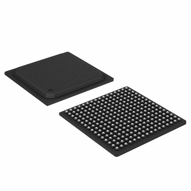
Pin Diagram . . . . . . . . . . . . . . . . . . . . . . . . . . . . . . . . . . . . . . . . . . . . . . . . . . . . . . . . . . . . . . . . . 203
Package Drawing for VSC8486SN-04 and VSC8486XSN-04 . . . . . . . . . . . . . . . . . . . . . . . . . . . 215
Package Drawing for VSC8486YSN-04 . . . . . . . . . . . . . . . . . . . . . . . . . . . . . . . . . . . . . . . . . . . . 216
Recommended Power Supply Isolation Schematic . . . . . . . . . . . . . . . . . . . . . . . . . . . . . . . . . . . 219
Split Plane Layout Example . . . . . . . . . . . . . . . . . . . . . . . . . . . . . . . . . . . . . . . . . . . . . . . . . . . . . 219
Decoupling Capacitor Placement Example . . . . . . . . . . . . . . . . . . . . . . . . . . . . . . . . . . . . . . . . . 220
VMDS-10298 VSC8486-04 Datasheet Revision 4.4
vii
�Tables
Table 1
Table 2
Table 3
Table 4
Table 5
Table 6
Table 7
Table 8
Table 9
Table 10
Table 11
Table 12
Table 13
Table 14
Table 15
Table 16
Table 17
Table 18
Table 19
Table 20
Table 21
Table 22
Table 23
Table 24
Table 25
Table 26
Table 27
Table 28
Table 29
Table 30
Table 31
Table 32
Table 33
Table 34
Table 35
Table 36
Table 37
Table 38
Table 39
Table 40
Table 41
Table 42
Table 43
Table 44
Table 45
Table 46
Table 47
Table 48
Table 49
Table 50
Table 51
Table 52
Table 53
Table 54
Pin Control for XGMII After Reset . . . . . . . . . . . . . . . . . . . . . . . . . . . . . . . . . . . . . . . . . . . . . . . . . . 10
MDIO Control for XGMII . . . . . . . . . . . . . . . . . . . . . . . . . . . . . . . . . . . . . . . . . . . . . . . . . . . . . . . . . 11
System Loopback Summary . . . . . . . . . . . . . . . . . . . . . . . . . . . . . . . . . . . . . . . . . . . . . . . . . . . . . . 11
System Loopback and XFI Traffic . . . . . . . . . . . . . . . . . . . . . . . . . . . . . . . . . . . . . . . . . . . . . . . . . . 12
Network Loopbacks Summary . . . . . . . . . . . . . . . . . . . . . . . . . . . . . . . . . . . . . . . . . . . . . . . . . . . . 12
Split Loopbacks Summary . . . . . . . . . . . . . . . . . . . . . . . . . . . . . . . . . . . . . . . . . . . . . . . . . . . . . . . 13
Retiming Clock Sources for Network and Split Loopbacks . . . . . . . . . . . . . . . . . . . . . . . . . . . . . . . 13
REFSEL0_STATUS Logic . . . . . . . . . . . . . . . . . . . . . . . . . . . . . . . . . . . . . . . . . . . . . . . . . . . . . . . 20
WAN Mode Control Logic . . . . . . . . . . . . . . . . . . . . . . . . . . . . . . . . . . . . . . . . . . . . . . . . . . . . . . . . 20
CMU and CRU Reference Clock Control and Frequency Summary . . . . . . . . . . . . . . . . . . . . . . . 21
LAN/SAN Configuration . . . . . . . . . . . . . . . . . . . . . . . . . . . . . . . . . . . . . . . . . . . . . . . . . . . . . . . . . 22
SONET/SDH Jitter Generation-Compliant Configuration . . . . . . . . . . . . . . . . . . . . . . . . . . . . . . . . 22
Non-SONET/SDH Jitter Generation-Compliant Configuration . . . . . . . . . . . . . . . . . . . . . . . . . . . . 23
SONET/SDH Jitter-Compliant Configuration . . . . . . . . . . . . . . . . . . . . . . . . . . . . . . . . . . . . . . . . . 23
XFI Transmitter Pre-emphasis Ratio . . . . . . . . . . . . . . . . . . . . . . . . . . . . . . . . . . . . . . . . . . . . . . . 26
CLK64AP/N Clock Output . . . . . . . . . . . . . . . . . . . . . . . . . . . . . . . . . . . . . . . . . . . . . . . . . . . . . . . . 27
CLK64BP/N Clock Output . . . . . . . . . . . . . . . . . . . . . . . . . . . . . . . . . . . . . . . . . . . . . . . . . . . . . . . . 27
Register 1×8002.14:11 RXINP/N Equalization Control . . . . . . . . . . . . . . . . . . . . . . . . . . . . . . . . . . 31
PMA LOS Register Status and Control Summary . . . . . . . . . . . . . . . . . . . . . . . . . . . . . . . . . . . . . 32
Section Overhead . . . . . . . . . . . . . . . . . . . . . . . . . . . . . . . . . . . . . . . . . . . . . . . . . . . . . . . . . . . . . . 35
Framing Parameter Description and Values . . . . . . . . . . . . . . . . . . . . . . . . . . . . . . . . . . . . . . . . . . 37
Line Overhead Octets . . . . . . . . . . . . . . . . . . . . . . . . . . . . . . . . . . . . . . . . . . . . . . . . . . . . . . . . . . . 41
K2 Encodings . . . . . . . . . . . . . . . . . . . . . . . . . . . . . . . . . . . . . . . . . . . . . . . . . . . . . . . . . . . . . . . . . 43
H1/H2 Pointer Types . . . . . . . . . . . . . . . . . . . . . . . . . . . . . . . . . . . . . . . . . . . . . . . . . . . . . . . . . . . 46
Concatenation Indication Types . . . . . . . . . . . . . . . . . . . . . . . . . . . . . . . . . . . . . . . . . . . . . . . . . . . 46
Pointer Interpreter State Diagram Transitions . . . . . . . . . . . . . . . . . . . . . . . . . . . . . . . . . . . . . . . . 47
STS Path Overhead Octets . . . . . . . . . . . . . . . . . . . . . . . . . . . . . . . . . . . . . . . . . . . . . . . . . . . . . . 48
RDI-P and ERDI-P Bit Settings and Interpretation . . . . . . . . . . . . . . . . . . . . . . . . . . . . . . . . . . . . . 51
PMTICK Counters . . . . . . . . . . . . . . . . . . . . . . . . . . . . . . . . . . . . . . . . . . . . . . . . . . . . . . . . . . . . . . 53
Defects and Anomalies . . . . . . . . . . . . . . . . . . . . . . . . . . . . . . . . . . . . . . . . . . . . . . . . . . . . . . . . . . 53
TOSI/ROSI Addresses . . . . . . . . . . . . . . . . . . . . . . . . . . . . . . . . . . . . . . . . . . . . . . . . . . . . . . . . . . 56
Control Codes . . . . . . . . . . . . . . . . . . . . . . . . . . . . . . . . . . . . . . . . . . . . . . . . . . . . . . . . . . . . . . . . . 60
E-PCS Logic . . . . . . . . . . . . . . . . . . . . . . . . . . . . . . . . . . . . . . . . . . . . . . . . . . . . . . . . . . . . . . . . . . 64
XAUI Lane LOS Threshold Summary . . . . . . . . . . . . . . . . . . . . . . . . . . . . . . . . . . . . . . . . . . . . . . . 67
XAUI Receiver Lane Equalization Setting . . . . . . . . . . . . . . . . . . . . . . . . . . . . . . . . . . . . . . . . . . . 67
XAUI Transmitter Lane Pre-emphasis Setting . . . . . . . . . . . . . . . . . . . . . . . . . . . . . . . . . . . . . . . . 70
MDIO-Manageable Device Addresses . . . . . . . . . . . . . . . . . . . . . . . . . . . . . . . . . . . . . . . . . . . . . . 72
Management Frame Format for Indirect Register Access . . . . . . . . . . . . . . . . . . . . . . . . . . . . . . . 73
XFP or SFP+ Host Application Pin Connections Summary . . . . . . . . . . . . . . . . . . . . . . . . . . . . . . 80
GPO Configuration Control Summary . . . . . . . . . . . . . . . . . . . . . . . . . . . . . . . . . . . . . . . . . . . . . . 82
JTAG TTL Signals . . . . . . . . . . . . . . . . . . . . . . . . . . . . . . . . . . . . . . . . . . . . . . . . . . . . . . . . . . . . . 83
TAP Controller States . . . . . . . . . . . . . . . . . . . . . . . . . . . . . . . . . . . . . . . . . . . . . . . . . . . . . . . . . . . 85
Supported Boundary Scan Test Instructions . . . . . . . . . . . . . . . . . . . . . . . . . . . . . . . . . . . . . . . . . 87
Boundary Scan Test Instruction Descriptions . . . . . . . . . . . . . . . . . . . . . . . . . . . . . . . . . . . . . . . . . 87
Device Identification Information . . . . . . . . . . . . . . . . . . . . . . . . . . . . . . . . . . . . . . . . . . . . . . . . . . . 88
Boundary Scan Register Bits . . . . . . . . . . . . . . . . . . . . . . . . . . . . . . . . . . . . . . . . . . . . . . . . . . . . . 88
Synchronous Ethernet Reference Clock Source . . . . . . . . . . . . . . . . . . . . . . . . . . . . . . . . . . . . . . 92
Synchronous Ethernet Register Bits . . . . . . . . . . . . . . . . . . . . . . . . . . . . . . . . . . . . . . . . . . . . . . . . 93
PMA_CTRL1: PMA Control 1 (1×0000) . . . . . . . . . . . . . . . . . . . . . . . . . . . . . . . . . . . . . . . . . . . . . 96
PMA_STAT1: PMA Status 1 (1×0001) . . . . . . . . . . . . . . . . . . . . . . . . . . . . . . . . . . . . . . . . . . . . . . 97
PMA_DEVID1: PMA Device Identifier 1 (1×0002) . . . . . . . . . . . . . . . . . . . . . . . . . . . . . . . . . . . . . 97
PMA_DEVID2: PMA Device Identifier 2 (1×0003) . . . . . . . . . . . . . . . . . . . . . . . . . . . . . . . . . . . . . 98
PMA_SPEED: PMA Speed Capability (1×0004) . . . . . . . . . . . . . . . . . . . . . . . . . . . . . . . . . . . . . . 98
PMA_DEVPKG1: PMA Devices in Package 1 (1×0005) . . . . . . . . . . . . . . . . . . . . . . . . . . . . . . . . 98
VMDS-10298 VSC8486-04 Datasheet Revision 4.4
viii
�Table 55
Table 56
Table 57
Table 58
Table 59
Table 60
Table 61
Table 62
Table 63
Table 64
Table 65
Table 66
Table 67
Table 68
Table 69
Table 70
Table 71
Table 72
Table 73
Table 74
Table 75
Table 76
Table 77
Table 78
Table 79
Table 80
Table 81
Table 82
Table 83
Table 84
Table 85
Table 86
Table 87
Table 88
Table 89
Table 90
Table 91
Table 92
Table 93
Table 94
Table 95
Table 96
Table 97
Table 98
Table 99
Table 100
Table 101
Table 102
Table 103
Table 104
Table 105
Table 106
Table 107
Table 108
Table 109
Table 110
Table 111
Table 112
Table 113
PMA_DEVPKG2: PMA Devices in Package 2 (1×0006) . . . . . . . . . . . . . . . . . . . . . . . . . . . . . . . . 99
PMA_CTRL2: PMA Control 2 (1×0007) . . . . . . . . . . . . . . . . . . . . . . . . . . . . . . . . . . . . . . . . . . . . . 99
PMA_STAT2: PMA Status 2 (1×0008) . . . . . . . . . . . . . . . . . . . . . . . . . . . . . . . . . . . . . . . . . . . . . . 99
PMA_CTRL3: PMA Control 3 (1×0009) . . . . . . . . . . . . . . . . . . . . . . . . . . . . . . . . . . . . . . . . . . . . 101
PMA_STAT3: PMA Status 3 (1×000A) . . . . . . . . . . . . . . . . . . . . . . . . . . . . . . . . . . . . . . . . . . . . . 101
Factory Test Register (1×000B-000D) . . . . . . . . . . . . . . . . . . . . . . . . . . . . . . . . . . . . . . . . . . . . . 101
PMA_PKGID1: PMA Package Identifier 1 (1×000E) . . . . . . . . . . . . . . . . . . . . . . . . . . . . . . . . . . 101
PMA_PKGID2: PMA Package Identifier 2 (1×000F) . . . . . . . . . . . . . . . . . . . . . . . . . . . . . . . . . . . 102
PMA_CFG1: PMA Configuration 1 (1×8000) . . . . . . . . . . . . . . . . . . . . . . . . . . . . . . . . . . . . . . . . 102
Factory Test Register (1×8001) . . . . . . . . . . . . . . . . . . . . . . . . . . . . . . . . . . . . . . . . . . . . . . . . . . 103
PMA_RXEQ_CTRL: PMA Rx Equalization Control (1×8002) . . . . . . . . . . . . . . . . . . . . . . . . . . . . 103
PMA_STAT4: PMA Status 4 (1×E600) . . . . . . . . . . . . . . . . . . . . . . . . . . . . . . . . . . . . . . . . . . . . . 103
PMA_CTRL4: PMA Control 4 (1×E601) . . . . . . . . . . . . . . . . . . . . . . . . . . . . . . . . . . . . . . . . . . . . 104
PMA_CTRL5: PMA Control 5 (1×E602) . . . . . . . . . . . . . . . . . . . . . . . . . . . . . . . . . . . . . . . . . . . . 104
High-Speed Data Output (Signal Quality Control) (1×E603) . . . . . . . . . . . . . . . . . . . . . . . . . . . . 105
Synchronous Ethernet Clock Control (1×E604) . . . . . . . . . . . . . . . . . . . . . . . . . . . . . . . . . . . . . . 106
DEV_CTRL3: DEVICE Control 3 (1×E605) . . . . . . . . . . . . . . . . . . . . . . . . . . . . . . . . . . . . . . . . . 106
DEV_STAT1: DEVICE Status 1 (1×E606) . . . . . . . . . . . . . . . . . . . . . . . . . . . . . . . . . . . . . . . . . . 108
DEV_STAT2: DEVICE Status 2 (1×E607) . . . . . . . . . . . . . . . . . . . . . . . . . . . . . . . . . . . . . . . . . . 109
PMA_LOS_ASSERT: PMA Loss of Signal Assert Control (1×E700) . . . . . . . . . . . . . . . . . . . . . . 110
PMA_LOS_DEASSERT: PMA Loss of Signal Deassert Control (1×E701) . . . . . . . . . . . . . . . . . 110
PMA_LOS_STAT: PMA Loss of Signal Status (1×E702) . . . . . . . . . . . . . . . . . . . . . . . . . . . . . . . 110
DEV_ID: DEVICE Identifier (1×E800) . . . . . . . . . . . . . . . . . . . . . . . . . . . . . . . . . . . . . . . . . . . . . . 111
DEV_REV: DEVICE Revision (1×E801) . . . . . . . . . . . . . . . . . . . . . . . . . . . . . . . . . . . . . . . . . . . . 111
Factory Test Register (1×E900) . . . . . . . . . . . . . . . . . . . . . . . . . . . . . . . . . . . . . . . . . . . . . . . . . . 111
DEV_GPIO_CTRL: DEVICE General Purpose I/O Control (1×E901) . . . . . . . . . . . . . . . . . . . . . 111
DEV_XFP_CTRL: DEVICE XFP Control (1×E902) . . . . . . . . . . . . . . . . . . . . . . . . . . . . . . . . . . . 112
Factory Test Register (1×EC00) . . . . . . . . . . . . . . . . . . . . . . . . . . . . . . . . . . . . . . . . . . . . . . . . . . 113
Factory Test (1×EC01–EC34) . . . . . . . . . . . . . . . . . . . . . . . . . . . . . . . . . . . . . . . . . . . . . . . . . . . 113
Factory Test (1×ED00–ED0F) . . . . . . . . . . . . . . . . . . . . . . . . . . . . . . . . . . . . . . . . . . . . . . . . . . . 113
Factory Test Register (1×EF00) . . . . . . . . . . . . . . . . . . . . . . . . . . . . . . . . . . . . . . . . . . . . . . . . . . 113
DEV_RST_CTRL: DEVICE Block Reset Control (1×EF01) . . . . . . . . . . . . . . . . . . . . . . . . . . . . . 114
DEV_XFI_CTRL2: DEVICE XFI Loopback Control 2 (1×EF10) . . . . . . . . . . . . . . . . . . . . . . . . . . 114
WIS_CTRL1: WIS Control 1 (2×0000) . . . . . . . . . . . . . . . . . . . . . . . . . . . . . . . . . . . . . . . . . . . . . 115
WIS_STAT1: WIS Status 1 (2×0001) . . . . . . . . . . . . . . . . . . . . . . . . . . . . . . . . . . . . . . . . . . . . . . 115
WIS_DEVID1: WIS Device Identifier 1 (2×0002) . . . . . . . . . . . . . . . . . . . . . . . . . . . . . . . . . . . . . 116
WIS_DEVID2: WIS Device Identifier 2 (2×0003) . . . . . . . . . . . . . . . . . . . . . . . . . . . . . . . . . . . . . 116
WIS_SPEED: WIS Speed Capability (2×0004) . . . . . . . . . . . . . . . . . . . . . . . . . . . . . . . . . . . . . . 116
WIS_DEVPKG1: WIS Devices in Package 1 (2×0005) . . . . . . . . . . . . . . . . . . . . . . . . . . . . . . . . 117
WIS_DEVPKG2: WIS Devices in Package 2 (2×0006) . . . . . . . . . . . . . . . . . . . . . . . . . . . . . . . . 117
WIS_CTRL2: WIS Control 2 (2×0007) . . . . . . . . . . . . . . . . . . . . . . . . . . . . . . . . . . . . . . . . . . . . . 117
WIS_STAT2: WIS Status 2 (2×0008) . . . . . . . . . . . . . . . . . . . . . . . . . . . . . . . . . . . . . . . . . . . . . . 118
WIS_TSTPAT_CNT: WIS Test Pattern Error Counter (2×0009) . . . . . . . . . . . . . . . . . . . . . . . . . 119
WIS_PKGID1: WIS Package Identifier 1 (2×000E) . . . . . . . . . . . . . . . . . . . . . . . . . . . . . . . . . . . 119
WIS_PKGID2: WIS Package Identifier 2 (2×000F) . . . . . . . . . . . . . . . . . . . . . . . . . . . . . . . . . . . . 119
WIS_STAT3: WIS Status 3 (2×0021) . . . . . . . . . . . . . . . . . . . . . . . . . . . . . . . . . . . . . . . . . . . . . . 119
WIS_REI_CNT: WIS Far-End Path Block Error Count (2×0025) . . . . . . . . . . . . . . . . . . . . . . . . . 120
WIS_TXJ1: WIS Tx J1s (2×0027-002E) . . . . . . . . . . . . . . . . . . . . . . . . . . . . . . . . . . . . . . . . . . . . 120
WIS_RXJ1: WIS Rx J1s (2×002F-0036) . . . . . . . . . . . . . . . . . . . . . . . . . . . . . . . . . . . . . . . . . . . . 121
WIS_REIL_CNT1: WIS Far-End Line BIP Errors 1 (2×0037) . . . . . . . . . . . . . . . . . . . . . . . . . . . . 121
WIS_REIL_CNT0: WIS Far-End Line BIP Errors 0 (2×0038) . . . . . . . . . . . . . . . . . . . . . . . . . . . . 121
WIS_B2_CNT1: WIS L-BIP Error Count 1 (2×0039) . . . . . . . . . . . . . . . . . . . . . . . . . . . . . . . . . . 121
WIS_B2_CNT0: WIS L-BIP Error Count 0 (2×003A) . . . . . . . . . . . . . . . . . . . . . . . . . . . . . . . . . . 122
WIS_B3_CNT: WIS P-BIP Block Error Count (2×003B) . . . . . . . . . . . . . . . . . . . . . . . . . . . . . . . . 122
WIS_B1_CNT: WIS S-BIP Error Count (2×003C) . . . . . . . . . . . . . . . . . . . . . . . . . . . . . . . . . . . . 122
WIS_TXJ0: WIS Transmit J0s (2×0040-0047) . . . . . . . . . . . . . . . . . . . . . . . . . . . . . . . . . . . . . . . 122
WIS_RXJ0: WIS Rx J0s (2×0048-004F) . . . . . . . . . . . . . . . . . . . . . . . . . . . . . . . . . . . . . . . . . . . . 122
EWIS_TXCTRL1: WIS Vendor-Specific Tx Control 1 (2×E600) . . . . . . . . . . . . . . . . . . . . . . . . . . 123
Factory Test Register (2×E601) . . . . . . . . . . . . . . . . . . . . . . . . . . . . . . . . . . . . . . . . . . . . . . . . . . 124
VMDS-10298 VSC8486-04 Datasheet Revision 4.4
ix
�Table 114
Table 115
Table 116
Table 117
Table 118
Table 119
Table 120
Table 121
Table 122
Table 123
Table 124
Table 125
Table 126
Table 127
Table 128
Table 129
Table 130
Table 131
Table 132
Table 133
Table 134
Table 135
Table 136
Table 137
Table 138
Table 139
Table 140
Table 141
Table 142
Table 143
Table 144
Table 145
Table 146
Table 147
Table 148
Table 149
Table 150
Table 151
Table 152
Table 153
Table 154
Table 155
Table 156
Table 157
Table 158
Table 159
Table 160
Table 161
Table 162
Table 163
Table 164
Table 165
Table 166
Table 167
Table 168
Table 169
Table 170
Table 171
Table 172
Factory Test Register (2×E602) . . . . . . . . . . . . . . . . . . . . . . . . . . . . . . . . . . . . . . . . . . . . . . . . . . 124
Factory Test Register (2×E603) . . . . . . . . . . . . . . . . . . . . . . . . . . . . . . . . . . . . . . . . . . . . . . . . . . 124
Factory Test Register (2×E604) . . . . . . . . . . . . . . . . . . . . . . . . . . . . . . . . . . . . . . . . . . . . . . . . . . 124
Factory Test Register (2×E605) . . . . . . . . . . . . . . . . . . . . . . . . . . . . . . . . . . . . . . . . . . . . . . . . . . 124
EWIS_TX_A1_A2: E-WIS Tx A1/A2 Octets (2×E611) . . . . . . . . . . . . . . . . . . . . . . . . . . . . . . . . . 125
EWIS_TX_Z0_E1: E-WIS Tx Z0/E1 Octets (2×E612) . . . . . . . . . . . . . . . . . . . . . . . . . . . . . . . . . 125
EWIS_TX_F1_D1: E-WIS Tx F1/D1 Octets (2×E613) . . . . . . . . . . . . . . . . . . . . . . . . . . . . . . . . . 125
EWIS_TX_D2_D3: E-WIS Tx D2/D3 Octets (2×E614) . . . . . . . . . . . . . . . . . . . . . . . . . . . . . . . . . 125
EWIS_TX_C2_H1: E-WIS Tx C2/H1 Octets (2×E615) . . . . . . . . . . . . . . . . . . . . . . . . . . . . . . . . . 125
EWIS_TX_H2_H3: E-WIS Tx H2/H3 Octets (2×E616) . . . . . . . . . . . . . . . . . . . . . . . . . . . . . . . . . 126
EWIS_TX_G1_K1: E-WIS Tx G1/K1 Octets (2×E617) . . . . . . . . . . . . . . . . . . . . . . . . . . . . . . . . . 126
EWIS_TX_K2_F2: E-WIS Tx K2/F2 Octets (2×E618) . . . . . . . . . . . . . . . . . . . . . . . . . . . . . . . . . 126
EWIS_TX_D4_D5: E-WIS Tx D4/D5 Octets (2×E619) . . . . . . . . . . . . . . . . . . . . . . . . . . . . . . . . . 126
EWIS_TX_D6_H4: E-WIS Tx D6/H4 Octets (2×E61A) . . . . . . . . . . . . . . . . . . . . . . . . . . . . . . . . . 126
EWIS_TX_D7_D8: E-WIS Tx D7/D8 Octets (2×E61B) . . . . . . . . . . . . . . . . . . . . . . . . . . . . . . . . . 127
EWIS_TX_D9_Z3: E-WIS Tx D9/Z3 Octets (2×E61C) . . . . . . . . . . . . . . . . . . . . . . . . . . . . . . . . . 127
EWIS_TX_D10_D11: E-WIS Tx D10/D11 Octets (2×E61D) . . . . . . . . . . . . . . . . . . . . . . . . . . . . 127
EWIS_TX_D12_Z4: E-WIS Tx D12/Z4 Octets (2×E61E) . . . . . . . . . . . . . . . . . . . . . . . . . . . . . . . 127
EWIS_TX_S1_Z1: E-WIS Tx S1/Z1 Octets (2×E61F) . . . . . . . . . . . . . . . . . . . . . . . . . . . . . . . . . 127
EWIS_TX_Z2_E2: E-WIS Tx Z2/E2 Octets (2×E620) . . . . . . . . . . . . . . . . . . . . . . . . . . . . . . . . . 128
EWIS_TX_N1: E-WIS Tx N1 Octet (2×E621) . . . . . . . . . . . . . . . . . . . . . . . . . . . . . . . . . . . . . . . . 128
Factory Test Register (2×E622) . . . . . . . . . . . . . . . . . . . . . . . . . . . . . . . . . . . . . . . . . . . . . . . . . . 128
EWIS_TX_MSGLEN: E-WIS Tx Trace Message Length Control (2×E700) . . . . . . . . . . . . . . . . . 128
EWIS_TXJ0: E-WIS Tx J0s 16-63 (2×E800-E817) . . . . . . . . . . . . . . . . . . . . . . . . . . . . . . . . . . . . 128
EWIS_RXJ0: E-WIS Rx J0s 16-63 (2×E900-E917) . . . . . . . . . . . . . . . . . . . . . . . . . . . . . . . . . . . 129
EWIS_TXJ1: E-WIS Tx WIS J1s 16-63 (2×EA00-EA17) . . . . . . . . . . . . . . . . . . . . . . . . . . . . . . . 129
EWIS_RXJ1: E-WIS Rx J1s 16-63 (2×EB00-EB17) . . . . . . . . . . . . . . . . . . . . . . . . . . . . . . . . . . . 129
EWIS_RX_FRM_CTRL1: E-WIS Rx Framer Control 1 (2×EC00) . . . . . . . . . . . . . . . . . . . . . . . . 129
EWIS_RX_FRM_CTRL2: E-WIS Rx Framer Control 2 (2×EC01) . . . . . . . . . . . . . . . . . . . . . . . . 130
EWIS_LOF_CTRL1: E-WIS Loss of Frame Control 1 (2×EC02) . . . . . . . . . . . . . . . . . . . . . . . . . 130
EWIS_LOF_CTRL2: E-WIS Loss of Frame Control 2 (2×EC03) . . . . . . . . . . . . . . . . . . . . . . . . . 131
EWIS_RX_CTRL1: E-WIS Rx Control 1 (2×EC10) . . . . . . . . . . . . . . . . . . . . . . . . . . . . . . . . . . . 131
EWIS_RX_MSGLEN: E-WIS Rx Trace Message Length Control (2×EC20) . . . . . . . . . . . . . . . . 132
EWIS_RX_ERR_FRC1: E-WIS Rx Error Force Control 1 (2×EC30) . . . . . . . . . . . . . . . . . . . . . . 132
EWIS_RX_ERR_FRC2: E-WIS Rx Error Force Control 2 (2×EC31) . . . . . . . . . . . . . . . . . . . . . . 133
EWIS_MODE_CTRL: E-WIS Mode Control (2×EC40) . . . . . . . . . . . . . . . . . . . . . . . . . . . . . . . . . 135
Factory Test Register (2×EC41) . . . . . . . . . . . . . . . . . . . . . . . . . . . . . . . . . . . . . . . . . . . . . . . . . . 135
EWIS_PRBS31_ANA_CTRL: E-WIS PRBS31 Analyzer Control (2×EC50) . . . . . . . . . . . . . . . . . 136
EWIS_PRBS31_ANA_STAT: E-WIS PRBS31 Analyzer Status (2×EC51) . . . . . . . . . . . . . . . . . 136
EWIS_PMTICK_CTRL: E-WIS Performance Monitor Control (2×EC60) . . . . . . . . . . . . . . . . . . . 137
EWIS_CNT_CFG: E-WIS Counter Configuration (2×EC61) . . . . . . . . . . . . . . . . . . . . . . . . . . . . . 137
EWIS_CNT_STAT: E-WIS Counter Status (2×EC62) . . . . . . . . . . . . . . . . . . . . . . . . . . . . . . . . . 138
EWIS_REIP_CNT1: E-WIS P-REI Counter 1 (MSW) (2×EC80) . . . . . . . . . . . . . . . . . . . . . . . . . 138
EWIS_REIP_CNT0: E-WIS P-REI Counter 0 (LSW) (2×EC81) . . . . . . . . . . . . . . . . . . . . . . . . . . 139
EWIS_REIL_CNT1: E-WIS L-REI Counter 1 (MSW) (2×EC90) . . . . . . . . . . . . . . . . . . . . . . . . . . 139
EWIS_REIL_CNT0: E-WIS L-REI Counter 0 (LSW) (2×EC91) . . . . . . . . . . . . . . . . . . . . . . . . . . 139
Factory Test Register (2×ECA0) . . . . . . . . . . . . . . . . . . . . . . . . . . . . . . . . . . . . . . . . . . . . . . . . . . 139
EWIS_B1_ERR_CNT1: E-WIS S-BIP Error Counter 1 (MSW) (2×ECB0) . . . . . . . . . . . . . . . . . . 139
EWIS_B1_ERR_CNT0: E-WIS S-BIP Error Counter 0 (LSW) (2×ECB1) . . . . . . . . . . . . . . . . . . . 140
EWIS_B2_ERR_CNT1: E-WIS L-BIP Error Counter 1 (MSW) (2×ECB2) . . . . . . . . . . . . . . . . . . 140
EWIS_B2_ERR_CNT0: E-WIS L-BIP Error Counter 0 (LSW) (2×ECB3) . . . . . . . . . . . . . . . . . . . 140
EWIS_B3_ERR_CNT1: E-WIS P-BIP Error Counter 1 (MSW) (2×ECB4) . . . . . . . . . . . . . . . . . . 140
EWIS_B3_ERR_CNT0: E-WIS P-BIP Error Counter 0 (LSW) (2×ECB5) . . . . . . . . . . . . . . . . . . . 140
Factory Test Register (2×ED00–ED08) . . . . . . . . . . . . . . . . . . . . . . . . . . . . . . . . . . . . . . . . . . . . 141
EWIS_RXTX_CTRL: E-WIS Rx to Tx Control (2×EE00) . . . . . . . . . . . . . . . . . . . . . . . . . . . . . . . 141
EWIS_PEND1: E-WIS Interrupt Pending 1 (2×EF00) . . . . . . . . . . . . . . . . . . . . . . . . . . . . . . . . . . 142
EWIS_MASKA_1: E-WIS Interrupt Mask A 1 (2×EF01) . . . . . . . . . . . . . . . . . . . . . . . . . . . . . . . . 144
EWIS_MASKB_1: E-WIS Interrupt Mask B 1 (2×EF02) . . . . . . . . . . . . . . . . . . . . . . . . . . . . . . . . 145
EWIS_INTR_STAT2: E-WIS Interrupt Status 2 (2×EF03) . . . . . . . . . . . . . . . . . . . . . . . . . . . . . . 146
VMDS-10298 VSC8486-04 Datasheet Revision 4.4
x
�Table 173
Table 174
Table 175
Table 176
Table 177
Table 178
Table 179
Table 180
Table 181
Table 182
Table 183
Table 184
Table 185
Table 186
Table 187
Table 188
Table 189
Table 190
Table 191
Table 192
Table 193
Table 194
Table 195
Table 196
Table 197
Table 198
Table 199
Table 200
Table 201
Table 202
Table 203
Table 204
Table 205
Table 206
Table 207
Table 208
Table 209
Table 210
Table 211
Table 212
Table 213
Table 214
Table 215
Table 216
Table 217
Table 218
Table 219
Table 220
Table 221
Table 222
Table 223
Table 224
Table 225
Table 226
Table 227
Table 228
Table 229
Table 230
Table 231
EWIS_INTR_PEND2: E-WIS Interrupt Pending 2 (2×EF04) . . . . . . . . . . . . . . . . . . . . . . . . . . . . 147
EWIS_INTR_MASKA2: E-WIS Interrupt Mask A 2 (2×EF05) . . . . . . . . . . . . . . . . . . . . . . . . . . . . 149
EWIS_INTR_MASKB2: E-WIS Interrupt Mask B 2 (2×EF06) . . . . . . . . . . . . . . . . . . . . . . . . . . . . 151
WIS Fault Control (2×EF07) . . . . . . . . . . . . . . . . . . . . . . . . . . . . . . . . . . . . . . . . . . . . . . . . . . . . . 152
PCS_CTRL1: PCS Control 1 (3×0000) . . . . . . . . . . . . . . . . . . . . . . . . . . . . . . . . . . . . . . . . . . . . . 153
PCS_STAT1: PCS Status 1 (3×0001) . . . . . . . . . . . . . . . . . . . . . . . . . . . . . . . . . . . . . . . . . . . . . 154
PCS_DEVID1: PCS Device Identifier 1 (3×0002) . . . . . . . . . . . . . . . . . . . . . . . . . . . . . . . . . . . . . 154
PCS_DEVID2: PCS Device Identifier 2 (3×0003) . . . . . . . . . . . . . . . . . . . . . . . . . . . . . . . . . . . . . 154
PCS_SPEED: PCS Speed Capability (3×0004) . . . . . . . . . . . . . . . . . . . . . . . . . . . . . . . . . . . . . . 154
PCS_DEVPKG1: PCS Devices in Package 1 (3×0005) . . . . . . . . . . . . . . . . . . . . . . . . . . . . . . . . 155
PCS_DEVPKG2: PCS Devices in Package 2 (3×0006) . . . . . . . . . . . . . . . . . . . . . . . . . . . . . . . . 155
PCS_CTRL2: PCS Control 2 (3×0007) . . . . . . . . . . . . . . . . . . . . . . . . . . . . . . . . . . . . . . . . . . . . . 155
PCS_STAT2: PCS Status 2 (3×0008) . . . . . . . . . . . . . . . . . . . . . . . . . . . . . . . . . . . . . . . . . . . . . 156
PCS_PKGID1: PCS Package Identifier 1 (3×000E) . . . . . . . . . . . . . . . . . . . . . . . . . . . . . . . . . . . 156
PCS_PKGID2: PCS Package Identifier 2 (3×000F) . . . . . . . . . . . . . . . . . . . . . . . . . . . . . . . . . . . 157
PCS_10GBASEX_STAT: PCS 10G BASE-X Status (3×0018) . . . . . . . . . . . . . . . . . . . . . . . . . . 157
PCS_10GBASEX_CTRL: PCS 10G BASE-X Control (3×0019) . . . . . . . . . . . . . . . . . . . . . . . . . . 157
PCS_10GBASER_STAT1: PCS 10G BASE-R Status 1 (3×0020) . . . . . . . . . . . . . . . . . . . . . . . . 157
PCS_10GBASER_STAT2: PCS 10G BASE-R Status 2 (3×0021) . . . . . . . . . . . . . . . . . . . . . . . . 158
PCS_SEEDA3: PCS Test Pattern Seed A 3 (3×0022) . . . . . . . . . . . . . . . . . . . . . . . . . . . . . . . . . 158
PCS_SEEDA2: PCS Test Pattern Seed A 2 (3×0023) . . . . . . . . . . . . . . . . . . . . . . . . . . . . . . . . . 158
PCS_SEEDA1: PCS Test Pattern Seed A 1 (3×0024) . . . . . . . . . . . . . . . . . . . . . . . . . . . . . . . . . 158
PCS_SEEDA0: PCS Test Pattern Seed A 0 (3×0025) . . . . . . . . . . . . . . . . . . . . . . . . . . . . . . . . . 158
PCS_SEEDB3: PCS Test Pattern Seed B 3 (3×0026) . . . . . . . . . . . . . . . . . . . . . . . . . . . . . . . . . 159
PCS_SEEDB2: PCS Test Pattern Seed B 2 (3×0027) . . . . . . . . . . . . . . . . . . . . . . . . . . . . . . . . . 159
PCS_SEEDB1: PCS Test Pattern Seed B 1 (3×0028) . . . . . . . . . . . . . . . . . . . . . . . . . . . . . . . . . 159
PCS_SEEDB0: PCS Test Pattern Seed B 0 (3×0029) . . . . . . . . . . . . . . . . . . . . . . . . . . . . . . . . . 159
PCS_TSTPAT_CTRL: PCS Test Pattern Control (3×002A) . . . . . . . . . . . . . . . . . . . . . . . . . . . . . 159
PCS_TSTPAT_CNT: PCS Test Pattern Error Counter (3×002B) . . . . . . . . . . . . . . . . . . . . . . . . . 160
PCS_USRPAT0: PCS User Test Pattern 0 (3×8000) . . . . . . . . . . . . . . . . . . . . . . . . . . . . . . . . . . 160
PCS_USRPAT1: PCS User Test Pattern 1 (3×8001) . . . . . . . . . . . . . . . . . . . . . . . . . . . . . . . . . . 160
PCS_USRPAT2: PCS User Test Pattern 2 (3×8002) . . . . . . . . . . . . . . . . . . . . . . . . . . . . . . . . . . 160
PCS_USRPAT3: PCS User Test Pattern 3 (3×8003) . . . . . . . . . . . . . . . . . . . . . . . . . . . . . . . . . . 161
PCS_SQPW_CTRL: PCS Square Wave Pulse Width Control (3×8004) . . . . . . . . . . . . . . . . . . . 161
PCS_CFG1: PCS Configuration 1 (3×8005) . . . . . . . . . . . . . . . . . . . . . . . . . . . . . . . . . . . . . . . . . 161
PCS_ERR_CNT0: PCS Test Error Counter 0 (3×8007) . . . . . . . . . . . . . . . . . . . . . . . . . . . . . . . . 162
PCS_ERR_CNT1: PCS Test Error Counter 1 (3×8008) . . . . . . . . . . . . . . . . . . . . . . . . . . . . . . . . 162
Factory Test Register (3×8009) . . . . . . . . . . . . . . . . . . . . . . . . . . . . . . . . . . . . . . . . . . . . . . . . . . 162
Factory Test Register (3×800C) . . . . . . . . . . . . . . . . . . . . . . . . . . . . . . . . . . . . . . . . . . . . . . . . . . 162
Factory Test Register (3×800D) . . . . . . . . . . . . . . . . . . . . . . . . . . . . . . . . . . . . . . . . . . . . . . . . . . 162
Factory Test Register (3×800E) . . . . . . . . . . . . . . . . . . . . . . . . . . . . . . . . . . . . . . . . . . . . . . . . . . 163
Factory Test Register (3×800F) . . . . . . . . . . . . . . . . . . . . . . . . . . . . . . . . . . . . . . . . . . . . . . . . . . 163
Factory Test Register (3×8010) . . . . . . . . . . . . . . . . . . . . . . . . . . . . . . . . . . . . . . . . . . . . . . . . . . 163
Factory Test Register (3×8011) . . . . . . . . . . . . . . . . . . . . . . . . . . . . . . . . . . . . . . . . . . . . . . . . . . 163
Factory Test Register (3×8012) . . . . . . . . . . . . . . . . . . . . . . . . . . . . . . . . . . . . . . . . . . . . . . . . . . 163
Factory Test Register (3×8013) . . . . . . . . . . . . . . . . . . . . . . . . . . . . . . . . . . . . . . . . . . . . . . . . . . 163
Factory Test Register (3×8014) . . . . . . . . . . . . . . . . . . . . . . . . . . . . . . . . . . . . . . . . . . . . . . . . . . 163
Factory Test Register (3×8015) . . . . . . . . . . . . . . . . . . . . . . . . . . . . . . . . . . . . . . . . . . . . . . . . . . 163
PCS_CFG2: PCS Configuration 2 (3×E600) . . . . . . . . . . . . . . . . . . . . . . . . . . . . . . . . . . . . . . . . 164
Factory Test Register (3×E601) . . . . . . . . . . . . . . . . . . . . . . . . . . . . . . . . . . . . . . . . . . . . . . . . . . 164
Factory Test Register (3×E602) . . . . . . . . . . . . . . . . . . . . . . . . . . . . . . . . . . . . . . . . . . . . . . . . . . 164
Factory Test Register (3×E603) . . . . . . . . . . . . . . . . . . . . . . . . . . . . . . . . . . . . . . . . . . . . . . . . . . 164
EPCS_STAT1: E-PCS Status 1 (3×E604) . . . . . . . . . . . . . . . . . . . . . . . . . . . . . . . . . . . . . . . . . . 164
EPCS_CORR_CNT: E-PCS Corrected FEC Error Counter (3×E605) . . . . . . . . . . . . . . . . . . . . . 165
EPCS_UCORR_CNT: E-PCS Uncorrected FEC Error Counter (3×E606) . . . . . . . . . . . . . . . . . . 165
EPCS_TXMSG: E-PCS Tx Message (3×E60A-E611) . . . . . . . . . . . . . . . . . . . . . . . . . . . . . . . . . 165
EPCS_RXMSG: E-PCS Rx Message (3×E612-E619) . . . . . . . . . . . . . . . . . . . . . . . . . . . . . . . . . 165
Factory Test Register (3×E61A) . . . . . . . . . . . . . . . . . . . . . . . . . . . . . . . . . . . . . . . . . . . . . . . . . . 166
Factory Test Register (3×E61B) . . . . . . . . . . . . . . . . . . . . . . . . . . . . . . . . . . . . . . . . . . . . . . . . . . 166
VMDS-10298 VSC8486-04 Datasheet Revision 4.4
xi
�Table 232
Table 233
Table 234
Table 235
Table 236
Table 237
Table 238
Table 239
Table 240
Table 241
Table 242
Table 243
Table 244
Table 245
Table 246
Table 247
Table 248
Table 249
Table 250
Table 251
Table 252
Table 253
Table 254
Table 255
Table 256
Table 257
Table 258
Table 259
Table 260
Table 261
Table 262
Table 263
Table 264
Table 265
Table 266
Table 267
Table 268
Table 269
Table 270
Table 271
Table 272
Table 273
Table 274
Table 275
Table 276
Table 277
Table 278
Table 279
Table 280
Table 281
Table 282
Table 283
Table 284
Table 285
Table 286
Table 287
Table 288
Table 289
Table 290
Factory Test Register (3×E61C) . . . . . . . . . . . . . . . . . . . . . . . . . . . . . . . . . . . . . . . . . . . . . . . . . . 166
Factory Test Register (3×E61D) . . . . . . . . . . . . . . . . . . . . . . . . . . . . . . . . . . . . . . . . . . . . . . . . . . 166
PHYXS_CTRL1: PHY XS Control 1 (4×0000) . . . . . . . . . . . . . . . . . . . . . . . . . . . . . . . . . . . . . . . 166
PHYXS_STAT1: PHY XS Status1 (4×0001) . . . . . . . . . . . . . . . . . . . . . . . . . . . . . . . . . . . . . . . . . 167
PHYXS_DEVID1: PHY XS Device Identifier 1 (4×0002) . . . . . . . . . . . . . . . . . . . . . . . . . . . . . . . 167
PHYXS_DEVID2: PHY XS Device Identifier 2 (4×0003) . . . . . . . . . . . . . . . . . . . . . . . . . . . . . . . 168
PHYXS_SPEED: PHY XS Speed Capability (4×0004) . . . . . . . . . . . . . . . . . . . . . . . . . . . . . . . . . 168
PHYXS_DEVPKG1: PHY XS Devices in Package 1 (4×0005) . . . . . . . . . . . . . . . . . . . . . . . . . . 168
PHYXS_DEVPKG2: PHY XS Devices in Package 2 (4×0006) . . . . . . . . . . . . . . . . . . . . . . . . . . 169
PHYXS_STAT2: PHY XS Status 2 (4×0008) . . . . . . . . . . . . . . . . . . . . . . . . . . . . . . . . . . . . . . . . 169
PHYXS_STAT3: PHY XS Status 3 (4×0018) . . . . . . . . . . . . . . . . . . . . . . . . . . . . . . . . . . . . . . . . 169
PHYXS_TSTCTRL1: PHY XGXS Test Control 1 (4×0019) . . . . . . . . . . . . . . . . . . . . . . . . . . . . . 170
PHYXS_TSTCTRL2: PHY XS Test Control 2 (4×8000) . . . . . . . . . . . . . . . . . . . . . . . . . . . . . . . . 170
PHYXS_TSTSTAT: PHY XS Test Pattern Check Status (4×8001) . . . . . . . . . . . . . . . . . . . . . . . 171
Factory Test Register (4×8002) . . . . . . . . . . . . . . . . . . . . . . . . . . . . . . . . . . . . . . . . . . . . . . . . . . 171
Factory Test Register (LSW) (4×8003) . . . . . . . . . . . . . . . . . . . . . . . . . . . . . . . . . . . . . . . . . . . . . 171
Factory Test Register (4×8004) . . . . . . . . . . . . . . . . . . . . . . . . . . . . . . . . . . . . . . . . . . . . . . . . . . 172
Factory Test Register (4×8005) . . . . . . . . . . . . . . . . . . . . . . . . . . . . . . . . . . . . . . . . . . . . . . . . . . 172
Factory Test Register (4×8006) . . . . . . . . . . . . . . . . . . . . . . . . . . . . . . . . . . . . . . . . . . . . . . . . . . 172
Factory Test Register (4×8007) . . . . . . . . . . . . . . . . . . . . . . . . . . . . . . . . . . . . . . . . . . . . . . . . . . 172
Factory Test Register (4×8008) . . . . . . . . . . . . . . . . . . . . . . . . . . . . . . . . . . . . . . . . . . . . . . . . . . 172
Factory Test Register (4×8009) . . . . . . . . . . . . . . . . . . . . . . . . . . . . . . . . . . . . . . . . . . . . . . . . . . 172
Factory Test Register (4×800A) . . . . . . . . . . . . . . . . . . . . . . . . . . . . . . . . . . . . . . . . . . . . . . . . . . 172
PHYXS_TPERR_CTRL: PHY XS Test Pattern Error Counter Control (4×800B) . . . . . . . . . . . . . 172
PHYXS_TPERR_CNT0: PHY XS Test Pattern Error Counter 0 (LSW) (4×800C) . . . . . . . . . . . . 173
PHYXS_TPERR_CNT0: PHY XS Test Pattern Error Counter 1 (MSW) (4×800D) . . . . . . . . . . . 173
PHYXS_XAUI_CTRL1: PHY XS XAUI Control 1 (4×800E) . . . . . . . . . . . . . . . . . . . . . . . . . . . . . 173
PHYXS_XAUI_CTRL2: PHY XS XAUI Control 2 (4×800F) . . . . . . . . . . . . . . . . . . . . . . . . . . . . . 174
PHYXS_RXEQ_CTRL: PHY XS XAUI Rx Equalization Control (4×8010) . . . . . . . . . . . . . . . . . . 175
PHYXS_TXPE_CTRL: PHY XS XAUI Tx Pre-emphasis Control (4×8011) . . . . . . . . . . . . . . . . . 175
PHYXS_RXLOS_STAT: PHY XS Rx Loss of Signal Status (4×8012) . . . . . . . . . . . . . . . . . . . . . 176
PHYXS_RXSD_STAT: PHY XS Rx Signal Detect Status (4×E600) . . . . . . . . . . . . . . . . . . . . . . 176
Factory Test Register (4×E601) . . . . . . . . . . . . . . . . . . . . . . . . . . . . . . . . . . . . . . . . . . . . . . . . . . 177
PHYXS_TXPD_CTRL: PHY XS XAUI Tx Power Down Control (4×E602) . . . . . . . . . . . . . . . . . . 177
PHYXS_RXPD_CTRL: PHY XS XAUI Rx Power Down Control (4×E603) . . . . . . . . . . . . . . . . . 178
FC_CJPAT_SEL (4×E604) . . . . . . . . . . . . . . . . . . . . . . . . . . . . . . . . . . . . . . . . . . . . . . . . . . . . . . 179
Factory Test Register (4×E610) . . . . . . . . . . . . . . . . . . . . . . . . . . . . . . . . . . . . . . . . . . . . . . . . . . 179
STW_CTRL1: STW Control 1 (1E×8000) . . . . . . . . . . . . . . . . . . . . . . . . . . . . . . . . . . . . . . . . . . . 179
STW_DEVADDR: STW Device Address (1E×8002) . . . . . . . . . . . . . . . . . . . . . . . . . . . . . . . . . . 180
STW_REGADDR: STW Register Address (1E×8003) . . . . . . . . . . . . . . . . . . . . . . . . . . . . . . . . . 180
STW_CFG1: STW Configuration 1 (1E×8004) . . . . . . . . . . . . . . . . . . . . . . . . . . . . . . . . . . . . . . . 180
NVR Memory Map (1E×8007-8106) . . . . . . . . . . . . . . . . . . . . . . . . . . . . . . . . . . . . . . . . . . . . . . . 181
DOM_RXALRM_CTRL: DOM Rx Alarm Control (1E×9000) . . . . . . . . . . . . . . . . . . . . . . . . . . . . 181
DOM_TXALRM_CTRL: DOM Tx Alarm Control (1E×9001) . . . . . . . . . . . . . . . . . . . . . . . . . . . . . 181
DOM_LASI_CTRL: DOM Link Alarm Status Interrupt Control (1E×9002) . . . . . . . . . . . . . . . . . . 182
DOM_RXALRM_STAT: DOM Rx Alarm Status (1E×9003) . . . . . . . . . . . . . . . . . . . . . . . . . . . . . 182
DOM_TXALRM_STAT: DOM Tx Alarm Status (1E×9004) . . . . . . . . . . . . . . . . . . . . . . . . . . . . . . 183
DOM_LASI_STAT: DOM Link Alarm Status Interrupt Status (1E×9005) . . . . . . . . . . . . . . . . . . . 183
DOM_TXFLAG_CTRL: DOM Tx Flag Control (1E×9006) . . . . . . . . . . . . . . . . . . . . . . . . . . . . . . 183
DOM_RXFLAG_CTRL: DOM Rx Flag Control (1E×9007) . . . . . . . . . . . . . . . . . . . . . . . . . . . . . . 184
Factory Test Register (1E×A000-A027) . . . . . . . . . . . . . . . . . . . . . . . . . . . . . . . . . . . . . . . . . . . . 184
Factory Test Register (1E×A048-A05F) . . . . . . . . . . . . . . . . . . . . . . . . . . . . . . . . . . . . . . . . . . . . 184
Factory Test Register (1E×A060-A06D) . . . . . . . . . . . . . . . . . . . . . . . . . . . . . . . . . . . . . . . . . . . . 184
Factory Test Register (1E×A06E) . . . . . . . . . . . . . . . . . . . . . . . . . . . . . . . . . . . . . . . . . . . . . . . . . 185
Factory Test Register (1E×A06F) . . . . . . . . . . . . . . . . . . . . . . . . . . . . . . . . . . . . . . . . . . . . . . . . . 185
DOM_TXALARM: DOM Tx Alarm Flags (1E×A070) . . . . . . . . . . . . . . . . . . . . . . . . . . . . . . . . . . . 185
DOM_RXALARM: DOM Rx Alarm Flags (1E×A071) . . . . . . . . . . . . . . . . . . . . . . . . . . . . . . . . . . 185
Factory Test Register (1E×A072-A073) . . . . . . . . . . . . . . . . . . . . . . . . . . . . . . . . . . . . . . . . . . . . 186
DOM_TXWARN: DOM Tx Warning Flags (1E×A074) . . . . . . . . . . . . . . . . . . . . . . . . . . . . . . . . . 186
VMDS-10298 VSC8486-04 Datasheet Revision 4.4
xii
�Table 291
Table 292
Table 293
Table 294
Table 295
Table 296
Table 297
Table 298
Table 299
Table 300
Table 301
Table 302
Table 303
Table 304
Table 305
Table 306
Table 307
Table 308
Table 309
Table 310
Table 311
Table 312
Table 313
Table 314
Table 315
Table 316
Table 317
Table 318
Table 319
Table 320
Table 321
Table 322
Table 323
Table 324
Table 325
Table 326
DOM_RXWARN: DOM Rx Warning Flags (1E×A075) . . . . . . . . . . . . . . . . . . . . . . . . . . . . . . . . . 186
Factory Test Register (1E×A076-A077) . . . . . . . . . . . . . . . . . . . . . . . . . . . . . . . . . . . . . . . . . . . . 187
Factory Test Register (1E×A0C0-A0FF) . . . . . . . . . . . . . . . . . . . . . . . . . . . . . . . . . . . . . . . . . . . . 187
Factory Test Register (1E×A100) . . . . . . . . . . . . . . . . . . . . . . . . . . . . . . . . . . . . . . . . . . . . . . . . . 187
Factory Test Register (1E×A101-A106) . . . . . . . . . . . . . . . . . . . . . . . . . . . . . . . . . . . . . . . . . . . . 187
LVTTL I/O Specifications . . . . . . . . . . . . . . . . . . . . . . . . . . . . . . . . . . . . . . . . . . . . . . . . . . . . . . . 188
Reference Clock Input Specifications . . . . . . . . . . . . . . . . . . . . . . . . . . . . . . . . . . . . . . . . . . . . . . 189
MDIO Interface Characteristics . . . . . . . . . . . . . . . . . . . . . . . . . . . . . . . . . . . . . . . . . . . . . . . . . . . 189
10-Gigabit Serial Data Input Specifications . . . . . . . . . . . . . . . . . . . . . . . . . . . . . . . . . . . . . . . . . 189
10-Gigabit Data Input Specifications for CRU . . . . . . . . . . . . . . . . . . . . . . . . . . . . . . . . . . . . . . . 191
10-Gigabit Data Output Specifications for MUX . . . . . . . . . . . . . . . . . . . . . . . . . . . . . . . . . . . . . . 193
10-Gigabit Data Output Specifications for CMU, WAN Mode . . . . . . . . . . . . . . . . . . . . . . . . . . . . 193
10-Gigabit Data Output Specifications for CMU, LAN/SAN Mode . . . . . . . . . . . . . . . . . . . . . . . . 194
XAUI Input Specifications . . . . . . . . . . . . . . . . . . . . . . . . . . . . . . . . . . . . . . . . . . . . . . . . . . . . . . . 196
XAUI Output Specifications . . . . . . . . . . . . . . . . . . . . . . . . . . . . . . . . . . . . . . . . . . . . . . . . . . . . . 197
XGMII Input Specifications . . . . . . . . . . . . . . . . . . . . . . . . . . . . . . . . . . . . . . . . . . . . . . . . . . . . . . 198
XGMII Output Specifications . . . . . . . . . . . . . . . . . . . . . . . . . . . . . . . . . . . . . . . . . . . . . . . . . . . . . 199
Reset Timing . . . . . . . . . . . . . . . . . . . . . . . . . . . . . . . . . . . . . . . . . . . . . . . . . . . . . . . . . . . . . . . . . 199
Reference Clock Specifications . . . . . . . . . . . . . . . . . . . . . . . . . . . . . . . . . . . . . . . . . . . . . . . . . . 199
TXCLK and RXCLK Timing Parameters . . . . . . . . . . . . . . . . . . . . . . . . . . . . . . . . . . . . . . . . . . . . 199
Recommended Operating Conditions . . . . . . . . . . . . . . . . . . . . . . . . . . . . . . . . . . . . . . . . . . . . . . 200
Stress Ratings . . . . . . . . . . . . . . . . . . . . . . . . . . . . . . . . . . . . . . . . . . . . . . . . . . . . . . . . . . . . . . . 201
XFI 10-Gigabit Data Bus Pins . . . . . . . . . . . . . . . . . . . . . . . . . . . . . . . . . . . . . . . . . . . . . . . . . . . . 204
XAUI 10-Gigabit Data Bus Pins . . . . . . . . . . . . . . . . . . . . . . . . . . . . . . . . . . . . . . . . . . . . . . . . . . 204
XGMII 10-Gigabit Data Bus Pins . . . . . . . . . . . . . . . . . . . . . . . . . . . . . . . . . . . . . . . . . . . . . . . . . 205
Serial Bus Interface Pins . . . . . . . . . . . . . . . . . . . . . . . . . . . . . . . . . . . . . . . . . . . . . . . . . . . . . . . 207
Input and Output Reference Clock Pins . . . . . . . . . . . . . . . . . . . . . . . . . . . . . . . . . . . . . . . . . . . . 208
Status and Control Pins . . . . . . . . . . . . . . . . . . . . . . . . . . . . . . . . . . . . . . . . . . . . . . . . . . . . . . . . 209
Phase Detector Output Pins . . . . . . . . . . . . . . . . . . . . . . . . . . . . . . . . . . . . . . . . . . . . . . . . . . . . . 210
Phase-Locked Loop Filter Capacitor Pins . . . . . . . . . . . . . . . . . . . . . . . . . . . . . . . . . . . . . . . . . . 211
JTAG Interface Pins . . . . . . . . . . . . . . . . . . . . . . . . . . . . . . . . . . . . . . . . . . . . . . . . . . . . . . . . . . . 211
Power and Ground Pins . . . . . . . . . . . . . . . . . . . . . . . . . . . . . . . . . . . . . . . . . . . . . . . . . . . . . . . . 211
Miscellaneous . . . . . . . . . . . . . . . . . . . . . . . . . . . . . . . . . . . . . . . . . . . . . . . . . . . . . . . . . . . . . . . . 213
Thermal Resistances . . . . . . . . . . . . . . . . . . . . . . . . . . . . . . . . . . . . . . . . . . . . . . . . . . . . . . . . . . 217
Power Supply and Pin Locations . . . . . . . . . . . . . . . . . . . . . . . . . . . . . . . . . . . . . . . . . . . . . . . . . 218
Ordering Information . . . . . . . . . . . . . . . . . . . . . . . . . . . . . . . . . . . . . . . . . . . . . . . . . . . . . . . . . . . 221
VMDS-10298 VSC8486-04 Datasheet Revision 4.4
xiii
�Revision History
1
Revision History
This section describes the changes that were implemented in this document. The changes are listed by
revision, starting with the most current publication.
1.1
Revision 4.4
In revision 4.4 of this document, the XAUI LOS signal information was clarified. For more information,
see Table 261, page 175 (bits 3:2) and Table 262, page 176 (bits 3:0).
1.2
Revision 4.3
In revision 4.3 of this document, the lead-free (Pb-free) package, VSC8486YSN-04, was added.
1.3
Revision 4.2
The following is a summary of the changes in revision 4.2 of this document.
•
•
1.4
Two-wire serial to SFP+/XFP manual mode of operation is not supported. The STW_MODE register
bit must be set to 0 for automatic mode of operation.
Two-wire serial reset command register was clarified. It can only be used to reset the local two-wire
serial circuit, not to reset downstream SFP+/XFP devices.
Revision 4.1
The following is a summary of the changes in revision 4.1 of this document.
•
•
1.5
The recommended operating temperature was changed from 0 °C ambient to 85 °C case to –40 °C
ambient to 95 °C case.
The minimum reference clock frequency was changed from 156.25 MHz to 153 MHz.
Revision 4.0
The following is a summary of the changes in revision 4.0 of this document.
•
•
•
•
•
•
1.6
Electrical specifications were updated based on final characterization results.
XGMII to XAUI mode is not supported.
The default value for the device revision number register 1×E801.15:0 was updated to 0×0004.
The PCS configuration register bit settings for 3×E600.1:0 were modified.
For applications that do not require high input gain, the synchronous Ethernet clock control register
bit 1×E604.15 should be set to 1 for optimal jitter tolerance.
The remote error indication (REI-P) status bit will be triggered in the event of an invalid REI-P value;
however, the REI-P counter will not be incremented.
Revision 2.0
Revision 2.0 was the first publication of this document.
VMDS-10298 VSC8486-04 Datasheet Revision 4.4
1
�Product Overview
2
Product Overview
The VSC8486-04 is a LAN/WAN XAUI or XGMII transceiver that converts 3 Gbps XAUI data to a
10 Gbps serial stream. At just 840 mW, the VSC8486-04 is ideal for applications requiring low power.
The device is also equipped with an additional full-rate data port that can be utilized for bypass
monitoring or channel monitoring applications. The device meets all specifications for 10 Gigabit
Ethernet (GbE) Layer-1 processing, as defined in IEEE 802.3ae.
The VSC8486-04 offers exceptional 10 Gbps mixed-signal performance with a data output that features
programmable pre-emphasis to enable longer traces of copper. The VSC8486-04 high-speed serial I/O
supports 9.9 Gbps, 10.3 Gbps, and 10.5 Gbps, as defined by IEEE 802.3ae and T11 10 GFC, and is fully
compliant with the SONET jitter specification defined by Bellcore GR253.
There are four main data processing blocks in the device: XGXS, PCS, WIS, and PMA. The 10 GbE
extender sublayer (XGXS) accepts 8b/10b data running at 3.125 Gbps and decodes it for transmission to
the physical coding sublayer (PCS). The XGXS is capable of deskewing more than 60 bit times between
lanes. The PCS receives data from the XGXS at 10 Gbps and encodes data according to the 64b/66b
algorithm described in IEEE 802.3ae clause 49.
The PCS features an optional extended mode (E-PCS) that also runs at the 64b/66b rate. This extended
mode uses an alternative framing algorithm that adds forward error correction (FEC) to provide ~2.5 dB
of net electrical coding gain. The E-PCS is available for LAN mode but not WAN mode.
The PCS outputs data to the WAN interface sublayer (WIS) when this mode is active (it is bypassed in
LAN mode). The WIS optionally takes data from the PCS at 9.953 Gbps and frames data in a SONET
STS-192c frame, as described in IEEE 802.3ae clause 50. Additionally, the WIS block contains extended
SONET and SDH processing capabilities that allow system operators to leverage valuable performance
monitoring data. Finally, data is delivered to the physical media attachment (PMA) block. The PMA
multiplexes the internal parallel data bus into a 10 Gbps data stream.
The 10 Gbps to XAUI data channel performs the operations described above in reverse. Notable
features in this path are a SONET-compliant LOS detector and a 10 Gbps receiver that is fully compliant
with XFI specifications, including stressed eye criteria.
The device operates using a 1.2 V supply dissipating only 750 mW in LAN mode and 840 mW in WAN
mode. The VSC8486-04 device is available in lead-free (Pb-free) packages, measuring 17 mm × 17 mm
with 256 pins and 1 mm pin pitch.
2.1
Features
The following list provides the features and benefits of the VSC8486-04 device.
2.1.1
Low Power
•
2.1.2
Wide Range of Support
•
•
•
•
•
2.1.3
Exceptionally low power (750 mW LAN mode or 840 mW WAN mode) allows for higher port
densities
Fully compatible with IEEE 802.3ae and T11 10 GFC
Extended-WIS (E-WIS) provides full Clause 50 support and enables transport over existing SONET
networks
10 Gbps serial interface exceeds all SONET and 10 GbE requirements
4 × 3.125 Gbps and 3.182 Gbps XAUI I/O enable interconnection with a wide range of Layer-2
devices
Seamless connectivity to XFP and SFP+ modules
Tools for Rapid Design
•
•
Multiple loopback modes and built-in self test (BIST) capabilities reduce system development costs,
enable manufacturing tests, and improve time to market
JTAG access port facilitates boundary scan for in-circuit test to improve board yield
VMDS-10298 VSC8486-04 Datasheet Revision 4.4
2
�Product Overview
•
2.1.4
Single 1.2 voltage for the whole device with optional power supply range (1.2 V, 1.5 V, 1.8 V, or
3.3 V) for the TTL interface
Flexibility
•
•
•
•
•
XAUI I/O programmability for lane swap, invert, amplitude, pre-emphasis, and equalization
KX4-compatible 3 Gbps I/O for long-reach copper interconnect provides additional margin to
traverse connectors and the backplane up to 40 inches
Extended-PCS (E-PCS) mode with forward error correction (FEC) auto-negotiation allows extended
reach over single-mode and multimode fiber with 10–15 error floor
On the 10-gigabit serial link, enhanced de-emphasis and equalization compensates for connector
and channel losses and makes the device SFP+ compatible
Accessibility of the recovered clock from high speed input and separate clock paths for CMU and
CRU enable Layer 1 support for Synchronous Ethernet
VMDS-10298 VSC8486-04 Datasheet Revision 4.4
3
�Functional Descriptions
3
Functional Descriptions
This section presents the functional description for the VSC8486-04 device. The main areas described
are:
•
•
•
•
•
3.1
Data paths
Loopback options
Implementation of the IEEE MDIO manageable devices (MMDs)
Extended functionality for WIS and PCS
Low-speed serial interfaces (MDIO, two-wire serial, and JTAG)
Operating Modes
The following illustration shows the VSC8486-04 operations.
VMDS-10298 VSC8486-04 Datasheet Revision 4.4
4
�XRX1P
VMDS-10298 VSC8486-04 Datasheet Revision 4.4
XAUI
XTX3N
XTX3P
XTX2N
XTX2P
XTX1N
XTX1P
XTX0N
XTX0P
REFCLKN
REFCLKP
XRX3N
XRX3P
XRX2N
XRX2P
XRX1N
CMU
MUX
XAUI
PLL
DIV
ENCODE
8B/10B
CRU
DEMUX
DIV
DECODE
10B/8B
XGMII
RXCLK RXD/C
W
FIFO
R
W
E-LAN
OR
DECODE
66B/64B
R
FIFO
E-PCS
GEAR
BOX
E-LAN
OR
ENCODE
64B/66B
GEAR
BOX
E-WIS
EXTRACT
E-WIS
FRAMER
FIFO
E-WIS
DEMUX
CMU
MUX
CRU
PMA
RXINN
RXINP
XFI
TXDOUTN
TXDOUTP
XAUI to XFI Mode
TXCLK
3.1.1
XRX0N
PHY-XS
Functional Block Diagram
XRX0P
XAUI
XGMII
Figure 1 •
TXD/C
Functional Descriptions
To put the VSC8486-04 in the XAUI to XFI mode, set the I/O mode select pin high (IOMODESEL = 1).
IOMODESEL sets the default value of XGMII_OE (3×8005.6) and PCS_XGMII_SRC (3×8005.8).
5
�Functional Descriptions
Figure 2 •
XAUI
XAUI to XFI Mode Functional Diagram
PHY-XS
E-PCS
E-WIS
PMA
XRX0P
XRX0N
XRX1P
XRX1N
XRX2P
CRU
DEMUX
ENCODE
64B/66B
DECODE
10B/8B
FIFO
OR
XRX2N
E-LAN
XRX3P
W
FIFO
GEAR
BOX
TXDOUTP
MUX
E-WIS
FRAMER
TXDOUTN
R
XRX3N
DIV
REFCLKP
REFCLKN
CMU
XAUI
PLL
XFI
DIV
XTX0P
R
XTX0N
W
DECODE
66B/64B
XTX1P
XTX1N
XTX2P
XTX2N
CMU
MUX
ENCODE
8B/10B
FIFO
OR
GEAR
BOX
E-WIS
EXTRACT
RXINP
DEMUX
CRU
RXINN
E-LAN
XTX3P
XTX3N
XAUI
3.1.1.1
Transmit Operation for XAUI to XFI Mode
As shown in the preceding illustration, the PHY XS block receives four 8b/10b encoded 3.125 Gbps
(3.1875 Gbps in SAN mode) data lanes on pins XRX[3:0]P/N. The clock is recovered and the data is
deserialized on each of the four lanes. Synchronization is performed before the data is passed into the
10b/8b decoders. The decoded data and accompanying control bits are then presented to the FIFO. The
FIFO deskews the four lanes and presents the aligned data to the PCS.
The FIFO within the PCS transfers path timing from the PHY XS recovered clock to the PMA transmit
clock by adding or deleting idle characters during inter-packet gaps (IPG) as needed. The eight data
octets (8-bit characters) and eight control bits pass through the 64b/66b encoder, which maps XGMII
data to a single 66-bit transmission block, as defined in Figure 49-7 of IEEE Standard 802.3ae.
In standard PCS mode (EPCS = 0), the first two bits of the 66-bit block contain the sync header, which is
used to establish block boundaries for the synchronization process during the receive operation. The
remaining 64 bits contain the payload. The payload passes through the scrambler, which implements the
polynomial G(x) = 1 + x39 + x58. The sync header bypasses the scrambler, and joins the scrambled
payload at the 64:66 gearbox. The gearbox adapts between the 66-bit width of the blocks and the 64-bit
width of the PMA or WIS interface.
In extended PCS mode (EPCS = 1), the 64 payload bits are mapped such that 24 instances of the 64-bit
payloads are placed into a larger 1584-bit frame defined by the Optical Internetworking Forum (OIF)
Common Electrical I/O Protocol (CEI-P). Each 64-bit payload is preceded by one transcoding bit, and the
remaining 24 bits of the 1584-bit frame are used for synchronization, fire code parity check, supervisory
channel, and to indicate the link state. This frame is then scrambled with a free-running linear feedback
shift register (LFSR) scrambler with a characteristic polynomial G(x) = x17 + x14 + 1. The scrambled
frame then passes through the 64:66 gearbox to the PMA or WIS.
In LAN or SAN mode (WAN_STAT = 0), the PCS data is passed directly to the PMA, while in WAN mode
(WAN_STAT = 1), the PCS data is passed to the WIS. The WIS inserts the PCS data into SONET STS192c/SDH STM-64 frames, and adds the required overhead.
Within the PMA, the data is serialized into the high-speed data stream (10.3125 Gbps in LAN mode,
10.51875 Gbps in SAN mode, and 9.95328 Gbps in WAN mode). The data stream and the divide-by-64
clock (161.13 MHz in LAN mode, 164.35 MHz in SAN mode, and 155.52 MHz in WAN mode) are
provided for line transmission on pins TXDOUTP/N and CLK64AP/N, respectively.
VMDS-10298 VSC8486-04 Datasheet Revision 4.4
6
�Functional Descriptions
3.1.1.2
Receive Operation for XAUI to XFI Mode
High-speed, 10 Gbps NRZ serial data is received on pins RXINP/N where it can be equalized for copper
trace dispersion and presented to the clock recovery unit (CRU).
In LAN and SAN mode (WAN_STAT = 0), the output of the CRU is deserialized and presented to the
PCS, while in WAN mode (WAN_STAT = 1), the output of the CRU is deserialized and presented to the
WIS. The WIS extracts the data from the SONET STS-192c/SDH STM-64 frames and processes the
overhead. The resultant data is then presented to the PCS.
In standard PCS mode (EPCS_STAT = 0), the data enters the 66:64 gearbox. The 66-bit block is then
aligned using the embedded 2-bit sync header, which generates the 64-bit payload. The payload is
descrambled using the polynomial G(x) = 1 + x39 + x58. The descrambled payload and 2-bit sync header
pass through the 64b/66b decoder, where the block is mapped to valid XGMII data, eight data octets, and
eight control bits.
In extended PCS mode (EPCS_STAT = 1), the data enters the PCS and is presented to the 66:64
gearbox. The data is then descrambled, framed, and formatted into 1584-bit frames. The Fire Code
parity check code in the received data stream is used to delineate frame boundaries. Because the
scrambler bits are XOR’ed with the FEC overhead during transmission, the state of the scrambler can be
recovered by subtracting the calculated parity from the received scrambled parity. The block is then
mapped to valid XGMII data, eight data octets, and eight control bits.
In both standard or extended PCS modes, the eight data octets and eight control bits are passed to the
FIFO, where path timing is transferred from the divided (one sixty-forth) recovered clock to the divided
(one sixty-sixth) CMU clock. During IPG, idle characters are added or deleted as necessary to adapt
between the two clock rates.
The eight data octets and eight control bits are then presented to the PHY XS block where it is 8b/10b
encoded and serialized. The serialized code words are then transmitted four at a time on the four XAUI
outputs: XTX[3:0]P/N.
3.1.2
XGMII to XFI Mode
To set the VSC8486-04 into the XGMII to XFI mode, the I/O mode select pin must be set low
(IOMODESEL = 0). IOMODESEL sets the default value of XGMII_OE (3×8005.6) and PCS_XGMII_SRC
(3×8005.8) appropriately to a value of 0×0140 after a reset is executed. The following illustration shows
the data path for this mode.
VMDS-10298 VSC8486-04 Datasheet Revision 4.4
7
�Functional Descriptions
Figure 3 •
XGMII to XFI Mode Functional Diagram
TXD31
E-PCS
TXD24
E-WIS
PMA
TXC3
TXD23
TXD16
ENCODE
64B/66B
TXC2
OR
TXD15
FIFO
TXD8
FIFO
GEAR
BOX
E-LAN
TXDOUTP
MUX
TXDOUTN
E-WIS
FRAMER
TXC1
TXD7
TXD0
R
W
TXCLK
REFCLKP
XGMII
RXCLK
XFI
CMU
TXC0
DIV
PLL
REFCLKN
R
RXD31
RXD24
W
RXC3
RXD23
RXD16
RXC2
FIFO
DECODE
66B/64B
RXD15
OR
RXD8
E-LAN
GEAR
BOX
E-WIS
EXTRACT
RXINP
DEMUX
CRU
RXINN
RXC1
RXD7
RXD0
RXC0
3.1.2.1
Transmit Operation for XGMII to XFI Mode
In XGMII to XFI mode, the XGXS (and XAUI input interface) is bypassed and the data is presented
directly to the PCS from the XGMII interface. All other transmit functions are the same.
3.1.2.2
Receive Operation for XGMII to XFI Mode
In XGMII to XFI mode, the XGXS (and XAUI output interface) is bypassed and the data from the PCS is
directly output from the device on the XGMII interface on RXD[31:0] and RXC[3:0].
3.2
Loopback
The VSC8486-04 LAN PHY has three 10-gigabit data ports: XAUI, XFI, and XGMII. There are several
options available to the user for routing traffic between the various ports. The purpose of this section is to
outline the operation of several modes loosely termed loopbacks. These modes can be extremely useful
for both test and debug purposes.
In addition to loopbacks, the device contains several pins that configure the device for XGMII or XAUI
operation without requiring MDIO access.
Loopback paths are shown in the following illustration.
VMDS-10298 VSC8486-04 Datasheet Revision 4.4
8
�XAUI
LPP_10B
4x800E.13
4x800F.0
4x0000.14
4x800E.13
XTX[3] (P)
XTX[3] (N)
XTX[2] (P)
XTX[2] (N)
XTX[1] (P)
XTX[1] (N)
XTX[0] (P)
XTX[0] (N)
XRX[3] (P)
XRX[3] (N)
XRX[2] (P)
XRX[2] (N)
XRX[1] (P)
XRX[1] (N)
XRX[0] (P)
XRX[0] (N)
A
VMDS-10298 VSC8486-04 Datasheet Revision 4.4
4x8000.2
4x8000.1
4x8000.0
“MIRROR”
XFI
0
1
B
PHY-XS
4x800F.11
4x800F.2
A
0
1
3x8005.8
LP_XGMII
1
D
1
0
“MIRROR”
XFI
3x8005.7
LP_XGMII
PATTERN
GENERATOR
0
1
C
0
PATTERN
CHECKER
4x800F.1
LP_XAUI
PHY-XS NETWORK LOOPBACK
IEEE 802.3ae Para 48.3.3
1
0
4x 1:10 DMUX
4x 10:1 MUX
4x800E.13
4x0000.14
10B/8B FIFO
C
XGMII
0
1
HSTL Output Drivers
Mux B
D
0
1
Mux A
HSTL Input Receivers
TXD[23:16]
TXC[2]
B
RXCLK
“SYSTEM”
8B/10B FIFO
TXCLK
TXD[7:0]
TXC[0]
RXD[7:0]
RXC[0]
“MIRROR”
XFI
XGMII
0
1
E
F
F
1
0
E-PCS
64B/66
Encoder &
Scrambler
H
0
1
G
0
1
1x8000.8
“MIRROR”
XFI
3x002A.5
31-1
(PRBS2 )
J
K
1
0
PMA
CRU
CMU
RXIN (N)
RXIN (P)
XFI
TXDOUT (N)
TXDOUT (P)
K
“XFI ONLY”
“NETWORK”
LP_XAUI: B and D
LPP_10B : B
LP_16B : G
LP_XGMII: PHY-XS from XGMII ingress,
XGMII outputs enabled
SPLITLOOPN: J and K
Primary Pin Loopback Control
0
1
FIFO &
Framer
Insertion
E-WIS
2xE600.0
Frame
Extraction
H
1
0
J
“00FF”
(repeating)
WIS SYSTEM LOOPBACK
IEEE 802.3ae Para. 50.3.9
SPLITLOOPN
2x0000.14
1x0000.0
PATT
CHECK
PATT
GEN
3x002A.4
31-1
(PRBS2 )
“MIRROR”
XFI
3x0000.14
LP_16B
LP_XGMII
3x8005.6
E-LAN
Firecode
Decoder
64B/66
Decoder &
Descrambler
E-Lan
Firecode
Encoder
G
“00FF”
(repeating)
PCS SYSTEM LOOPBACK
IEEE 802.3ae Para. 49.2.14.4
3x8005.3
3x8005.2
E
66/64
Gearbox
TXD[15:8]
TXC[1]
RXD[15:8]
RXC[1]
“00FF”
(repeating)
66/64
Gearbox
“MIRROR”
XAUI
FIFO
RXD[23:16]
RXC[2]
1:64 DMUX
TXD[31:24]
TXC[3]
FIFO
RXD[31:24]
RXC[3]
64:1 MUX
Figure 4 •
“MIRROR”
XAUI
Functional Descriptions
Loopback Configuration
Two split loopback paths (that is, two loopback paths simultaneously switched on) are enabled by the
SPLITLOOPN and LP_XAUI pins. Most other data path routing and loopback controls are enabled
through the MDIO interface.
9
�Functional Descriptions
3.2.1
Input/Output Mode Select and XGMII Mode
On power up or reset, the state of the IOMODESEL pin sets the VSC8486-04 data path routing on chip
as follows:
1.
On reset, if IOMODESEL = 0, then 3×8005.8:6 is set to 101. This setting programs multiplexers a
and b for XGMII mode and enables the XGMII output drivers.
On reset, if IOMODESEL = 1, 3×8005.8:6 is set to 000. This setting programs multiplexers a and b
for XAUI mode and disables the XGMII output.
2.
Mux a, mux b, and OE controls can also be configured after a reset, using the MDIO 3×8005.8:6 bits.
If LP_XGMII is pulled high, the XGMII output is enabled and the XGXS receives its data from the XGMII
input, TXD[31:0], regardless of the settings for IOMODESEL or the 3×8005.8:6 bits. The VSC8486-04
can be programmed to mirror XGMII Tx input data simultaneously to the PCS and the XGXS.
Alternatively, the PCS data can be routed simultaneously to the XGMII Rx output and the XGXS.
Figure 5 •
Data Path XGMII Source
XGMII TXD[31:0]
3×8005.8
LP_XGMII
1
Mux a
0
Loopback E
XGXS
1
PCS
Mux b
1
0
0
3×8005.2
3×8005.7
LP_XGMII
3×8005.6
LP_XGMII
OE
XGMII RXD[31:0]
The following table summarizes the control settings using the IOMODESEL pin.
Table 1 •
Pin Control for XGMII After Reset
IOMODESEL
Pin Control
XGMII
Data Source
XGXS
0
1
PCS
PCS
XGMII
Output Driver
Enabled?
3×8005 Register Value
Set on Reset
Bit 8
Bit 7
Bit 6
XGMII
TXD[31:0]
Yes
1
0
1
XGXS
No
0
0
0
VMDS-10298 VSC8486-04 Datasheet Revision 4.4
10
�Functional Descriptions
The following table summarizes control settings using the MDIO registers, where XGMII output is always
from PCS.
Table 2 •
3.2.2
MDIO Control for XGMII
3×8005 MDIO
Register Settings
Data Source
Bit 8
Bit 7
Bit 6
PCS
XGXS
XGMII
Output
0
0
0
XGXS
PCS
Off
XGXS data comes from PCS, PCS
data comes from XGXS. XGMII output
drivers disabled.
0
0
1
XGXS
PCS
On
XGXS data comes from PCS, PCS
data comes from XGXS. XGMII RXD
comes from PCS. (Mirror PCS data to
XGMII.)
0
1
0
XGXS
XGMII
TXD
Off
XGXS data comes from XGMII TXD,
PCS data comes from XGXS. XGMII
output drivers disabled.
0
1
1
XGXS
XGMII
TXD
On
XGXS data comes from XGMII TXD,
PCS data comes from XGXS. XGMII
RXD comes from PCS.
1
0
0
XGMII
TXD
PCS
Off
XGXS data comes from PCS, PCS
data comes from XGMII TXD. XGMII
output drivers disabled.
1
0
1
XGMII
TXD
PCS
On
XGXS data comes from PCS, PCS
data comes from XGMII TXD. XGMII
RXD comes from PCS. (Mirror PCS
data to XGMII.)
1
1
0
XGMII
TXD
XGMII
TXD
Off
XGXS data comes from XGMII TXD,
PCS data comes from XGMII TXD.
XGMII output drivers disabled. (Mirror
XGMII TXD to XGXS.)
1
1
1
XGMII
TXD
XGMII
TXD
On
XGXS data comes from XGMII TXD,
PCS data comes from XGMII TXD.
XGMII RXD comes from PCS. (Mirror
XGMII TXD to XGXS.)
Description
Loopback Modes
There are three types of loopback modes: system, network, and split loopbacks. In general, system
loopbacks affect XAUI traffic, network loopbacks affect XFI traffic, and split loopbacks affect both. The
following table provides a summary of the system loopbacks.
Table 3 •
System Loopback Summary
Loopback Name
Loopback Enable
Retiming
B
PHY XS shallow
system loopback
Any of the following:
LPP_10B = 1
LP_XAUI = 1
4×800E.13 = 1
4×800F.0 = 0
Phase delay only, XAUI XTX[3:0]
signals retimed from XAUI
XRX[3:0] recovered clock
C
PHY XS deep system 4×800F.2 = 1
loopback
XAUI XTX[3:0] signals retimed to
LAN clock (REFCLKP/N)
VMDS-10298 VSC8486-04 Datasheet Revision 4.4
11
�Functional Descriptions
System Loopback Summary (continued)
Table 3 •
Loopback Name
Loopback Enable
Retiming
E
PCS FIFO system
loopback
3×8005.2 = 1
XAUI XTX[3:0] signals retimed to
LAN clock (REFCLKP/N)
G
PCS system loopback LP_16B = 1 or
3×0000.14 = 1
XAUI XTX[3:0] signals retimed to
LAN clock (REFCLKP/N)
J
PMA/WIS system
loopback
XAUI XTX[3:0] signals retimed to
LAN clock (REFCLKP/N)
Any of the following:
SPLITLOOPN = 0
(active low)
2×0000.14 = 1
1×0000.0 = 1
For system loopbacks, the XAUI data can be mirrored to the XFI Tx port, depending on the register
setting of XFI_LPBK_OVR (1×EF10.2).
Table 4 •
System Loopback and XFI Traffic
If XFI_LPBK_OVR
Loopback (1×EF10.2) = 01
If XFI_LPBK_OVR
(1×EF10.2) = 1
B
XFI Tx traffic from
WIS/PCS
XFI Tx traffic set by 1×EF10.1:0
00: 0×00FF pattern
01: All zeros
10: All ones
11: WIS/PCS
C
XFI Tx traffic from
WIS/PCS
XFI Tx traffic set by 1×EF10.1:0
00: 0×00FF pattern
01: All zeros
10: All ones
11: WIS/PCS
E, G, or J
0×00FF pattern
XFI Tx traffic set by 1×EF10.1:0
00: 0×00FF pattern
01: All zeros
10: All ones
11: WIS/PCS
1.
The XFI_LPBK_OVR (1×EF10.2) register defaults to 0.
The following table provides a summary of the network loopbacks, which primarily affect XFI traffic.
Table 5 •
Network Loopbacks Summary
Loopback Name
Loopback Enable
Retiming
A
PHY XS deep network
loopback
4×0000.14 = 1 and
4×800E.13 = 0
See Table 7, page 13
D
PHY XS shallow
network loopback
Any of the following:
4×800E.13 = 0 and
4×0000.14 = 0
4×800F.1 = 1
LP_XAUI = 1
See Table 7, page 13
F
PCS gearbox network
loopback
3×8005.3 = 1
See Table 7, page 13
H
WIS network loopback
2×E600.0 = 1
See Table 7, page 13
VMDS-10298 VSC8486-04 Datasheet Revision 4.4
12
�Functional Descriptions
Table 5 •
Network Loopbacks Summary (continued)
Loopback Name
Loopback Enable
K
Any of the following:
See Table 7, page 13
SPLITLOOPN = 0 (active low)
1×8000.8 = 0
PMA network loopback
Retiming
Split loopback affects both XAUI and XFI traffic. Split loopback is enabled using the LP_XAUI and
SPLITLOOPN pins, as shown in the following table.
Split Loopbacks Summary
Table 6 •
3.2.2.1
Loopback Name
Loopback Enable
Retiming
B and D
XAUI split loopback
LP_XAUI = 1
Internally pulled low
See Table 7, page 13
J and K
PMA split loopback
SPLITLOOPN = 0
Internally pulled high
See Table 7, page 13
Retiming Clock Sources for Network and Split Loopbacks
For network and split loopbacks, there are various options for controlling the XFI retiming, as shown in
the following table. For retiming XAUI traffic (pins XTX[3:0]), REFCLKP/N is used; however, when the
split loopback B and D is active, the recovered clock from XRX[3:0] is used.
Table 7 •
3.3
Retiming Clock Sources for Network and Split Loopbacks
WAN_STAT
(1×E606.15)
LINETIME_STAT
(1×E606.13)
XFI Retimed With
0
0
REFCLKP/N
0
1
10G LINE_IN
1
0
WREFCLKP/N
1
1
10G LINE_IN
Loopback Paths
This section describes each loopback, listed in alphabetical order.
3.3.1
Loopback A
Loopback A is located in the XAUI PHY. It reroutes the data from the 10:1 MUX in the XAUI PHY into the
1:10 DEMUX, as shown in the following illustration.
VMDS-10298 VSC8486-04 Datasheet Revision 4.4
13
�Functional Descriptions
Figure 6 •
PHY XS Deep Network Loopback
XGMII
XAUI
XRX[0] (N)
PHY-XS
XRX[0] (P)
WIS
PMA
XTX[2] (N)
XTX[2] (P)
XTX[3] (N)
FIFO
F
FIFO &
Framer
Insertion
G
1
0
8B/10B FIFO
4X 10:1 MUX
XTX[1] (P)
Mux B
D
E-LAN
Firecode
Encoder
64B/66
Decoder &
DeScrambler
K
Frame
Extraction
E-LAN
Firecode
Decoder
XTX[3] (P)
TXDOUT (N)
TXDOUT (P)
J
H
CMU
1:64 DEMUX
C
B
A
XTX[0] (P)
XTX[1] (N)
E
66/64
Gearbox
XRX[3] (P)
0
66/64
Gearbox
XRX[3] (N)
64B/66
Encoder &
Scrambler
1
FIFO
XRX[2] (P)
10B/8B FIFO
4X 1:10 DEMUX
XRX[2] (N)
64:1 MUX
Mux A
XRX[1] (P)
XTX[0] (N)
PCS
HSTL Input Receivers
XRX[1] (N)
XFI
RXIN (N)
RXIN (P)
CRU
HSTL Output Drivers
XGMII
XFI data is retimed with PMA CRU. To enable loopback A, set both of the following: LPBK_A
(4×0000.14) set to 1 and LPBK_B (4×800E.13) set to 0. The default value for bit 14 is 0 (loopback
disabled). XFI ingress (RXINP/N) data is mirrored to the XAUI egress port (XTX[3:0]P/N) simultaneously
without further MDIO instructions. This loopback cannot be used if LP_XAUI is asserted high.
Note: For loopback A to function without a XAUI input present, the XS Rx signal detect register 4×E600.1 must
be set to 1 in order for the XAUI inputs to sync up.
3.3.2
Loopback B
Loopback B routes the incoming XAUI data through the 1:10 DEMUX and then loops back before the
10b/8b decoder into the 10:1 MUX. Data is retimed by the recovered XAUI clock. No 10b/8b decoding or
lane synchronization is performed. System XAUI data is also mirrored to the XFI Tx port. To enable
loopback B, set the LPBK_B register (4×800E.13) to 1, the LPP_10B pin to high, or the LP_XAUI pin to
high. The LP_XAUI pin setting simultaneously enables loopback D.
Figure 7 •
PHY XS Shallow System Loopback
XGMII
XAUI
XRX[0] (N)
PHY-XS
XRX[0] (P)
XTX[3] (N)
F
XTX[3] (P)
FIFO &
Framer
Insertion
G
66/64
Gearbox
FIFO
0
64B/66
Decoder &
DeScrambler
64:1 MUX
E-LAN
Firecode
Encoder
1
8B/10B FIFO
XTX[2] (P)
Mux B
D
4X 10:1 MUX
XTX[2] (N)
64B/66
Encoder &
Scrambler
E
C
B
A
XTX[0] (P)
XTX[1] (P)
PMA
TXDOUT (N)
TXDOUT (P)
J
K
H
Frame
Extraction
E-LAN
Firecode
Decoder
CMU
1:64 DEMUX
XRX[3] (P)
0
66/64
Gearbox
XRX[3] (N)
1
FIFO
XRX[2] (P)
10B/8B FIFO
4X 1:10 DEMUX
XRX[2] (N)
XTX[1] (N)
WIS
Mux A
XRX[1] (P)
XTX[0] (N)
PCS
HSTL Input Receivers
XRX[1] (N)
CRU
XFI
RXIN (N)
RXIN (P)
HSTL Output Drivers
XGMII
3.3.3
Loopback C
Loopback C routes the incoming XAUI data after the 10b/8b FIFO back into the 8b/10b FIFO. System
XAUI data is also mirrored to the XFI Tx port. To enable loopback C, set LPBK_C (4×800F.2) to 1.
VMDS-10298 VSC8486-04 Datasheet Revision 4.4
14
�Functional Descriptions
Figure 8 •
PHY XS Deep System Loopback
XGMII
XAUI
XRX[0] (N)
PHY-XS
XRX[0] (P)
WIS
PMA
E
C
B
A
64B/66
Encoder &
Scrambler
Mux B
F
D
XTX[0] (P)
E-LAN
Firecode
Encoder
FIFO &
Framer
Insertion
G
XTX[2] (P)
XTX[3] (N)
64B/66
Decoder &
DeScrambler
FIFO
XTX[2] (N)
8B/10B FIFO
4X 10:1 MUX
XTX[1] (P)
0
K
Frame
Extraction
E-LAN
Firecode
Decoder
XTX[3] (P)
TXDOUT (N)
TXDOUT (P)
J
H
66/64
Gearbox
1
XTX[1] (N)
CMU
1:64 DEMUX
XRX[3] (P)
0
66/64
Gearbox
XRX[3] (N)
1
FIFO
XRX[2] (P)
10B/8B FIFO
4X 1:10 DEMUX
XRX[2] (N)
64:1 MUX
Mux A
XRX[1] (P)
XTX[0] (N)
PCS
HSTL Input Receivers
XRX[1] (N)
XFI
RXIN (N)
RXIN (P)
CRU
HSTL Output Drivers
XGMII
3.3.4
Loopback D
Loopback D routes the incoming XFI data after the PCS FIFO back into the transmit PCS FIFO. Network
XFI Rx data is also mirrored to the XAUI egress port. To enable loopback D, set either the LPBK_D
register (4×800F.1) to 1, both the LPBK_B (4×800E.13) and LPBK_A (4×0000.14) registers to 1, or the
LP_XAUI pin to high. The LP_XAUI pin setting simultaneously enables loopback B.
Figure 9 •
PHY XS Shallow Network Loopback
XGMII
XAUI
XRX[0] (N)
PHY-XS
XRX[0] (P)
XTX[3] (N)
F
XTX[3] (P)
FIFO &
Framer
Insertion
G
66/64
Gearbox
FIFO
0
64B/66
Decoder &
DeScrambler
64:1 MUX
E-LAN
Firecode
Encoder
1
8B/10B FIFO
XTX[2] (P)
Mux B
D
4X 10:1 MUX
XTX[2] (N)
64B/66
Encoder &
Scrambler
E
C
B
A
XTX[0] (P)
XTX[1] (P)
PMA
TXDOUT (N)
TXDOUT (P)
J
K
H
Frame
Extraction
E-LAN
Firecode
Decoder
CMU
1:64 DEMUX
XRX[3] (P)
0
66/64
Gearbox
XRX[3] (N)
1
FIFO
XRX[2] (P)
10B/8B FIFO
4X 1:10 DEMUX
XRX[2] (N)
XTX[1] (N)
WIS
Mux A
XRX[1] (P)
XTX[0] (N)
PCS
HSTL Input Receivers
XRX[1] (N)
CRU
XFI
RXIN (N)
RXIN (P)
HSTL Output Drivers
XGMII
3.3.5
Loopback E
Loopback E routes the incoming XAUI data from the PCS transmit FIFO back into the PCS receive FIFO.
The data transmitted to the XFI Tx port is a continuous stream of 0×00FF data words. To enable
loopback E, set LPBK_E (3×8005.2) to 1.
VMDS-10298 VSC8486-04 Datasheet Revision 4.4
15
�Functional Descriptions
Figure 10 • PCS FIFO System Loopback
XGMII
XAUI
XRX[0] (N)
PHY-XS
XRX[0] (P)
WIS
PMA
Mux A
XRX[3] (P)
E
C
B
A
64B/66
Encoder &
Scrambler
Mux B
F
D
XTX[0] (P)
E-LAN
Firecode
Encoder
FIFO &
Framer
Insertion
G
XTX[2] (P)
XTX[3] (N)
FIFO
XTX[2] (N)
0
8B/10B FIFO
4X 10:1 MUX
XTX[1] (P)
64B/66
Decoder &
DeScrambler
K
Frame
Extraction
E-LAN
Firecode
Decoder
XTX[3] (P)
TXDOUT (N)
TXDOUT (P)
J
H
66/64
Gearbox
1
XTX[1] (N)
“00FF”
64:1 MUX
0
CMU
1:64 DEMUX
XRX[3] (N)
1
66/64
Gearbox
XRX[2] (P)
FIFO
XRX[2] (N)
10B/8B FIFO
4X 1:10 DEMUX
XRX[1] (P)
XTX[0] (N)
PCS
HSTL Input Receivers
XRX[1] (N)
XFI
RXIN (N)
RXIN (P)
CRU
HSTL Output Drivers
XGMII
3.3.6
Loopback F
Loopback F routes the incoming XFI data after the receive PCS gearbox back into the transmit PCS
gearbox. Network XFI Rx data is also mirrored to the XAUI egress port. To enable loopback F, set
LPBK_F (3×8005.3) to 1.
Figure 11 • Gearbox Network Loopback
XGMII
XAUI
XRX[0] (N)
PHY-XS
XRX[0] (P)
WIS
PMA
Mux A
XRX[3] (P)
E
C
B
A
64B/66
Encoder &
Scrambler
Mux B
F
D
XTX[0] (P)
E-LAN
Firecode
Encoder
FIFO &
Framer
Insertion
G
XTX[2] (P)
XTX[3] (N)
FIFO
XTX[2] (N)
8B/10B FIFO
4X 10:1 MUX
XTX[1] (P)
0
64B/66
Decoder &
DeScrambler
66/64
Gearbox
1
XTX[1] (N)
TXDOUT (N)
TXDOUT (P)
J
K
H
Frame
Extraction
E-LAN
Firecode
Decoder
XTX[3] (P)
“00FF”
64:1 MUX
0
CMU
1:64 DEMUX
XRX[3] (N)
1
66/64
Gearbox
XRX[2] (P)
FIFO
XRX[2] (N)
10B/8B FIFO
4X 1:10 DEMUX
XRX[1] (P)
XTX[0] (N)
PCS
HSTL Input Receivers
XRX[1] (N)
XFI
RXIN (N)
RXIN (P)
CRU
HSTL Output Drivers
XGMII
3.3.7
Loopback G
Loopback G routes the incoming XAUI data through the PCS transmit gearbox back into the PCS receive
gearbox. The data transmitted to the XFI Tx port is a continuous stream of 0×00FF data words. To enable
loopback G, either set LPBK_G (3×0000.14) to 1 or set the LP_16B pin high.
Figure 12 • PCS System Loopback G
XGMII
XAUI
XRX[0] (N)
PHY-XS
XRX[0] (P)
XTX[3] (N)
XTX[3] (P)
PMA
0
64B/66
Decoder &
DeScrambler
G
FIFO
“00FF”
64:1 MUX
E-LAN
Firecode
Encoder
FIFO &
Framer
Insertion
TXDOUT (N)
TXDOUT (P)
J
K
H
Frame
Extraction
E-LAN
Firecode
Decoder
CMU
1:64 DEMUX
XTX[2] (P)
F
1
8B/10B FIFO
XTX[2] (N)
Mux B
D
4X 10:1 MUX
XTX[1] (P)
E
C
B
A
XTX[0] (P)
64B/66
Encoder &
Scrambler
66/64
Gearbox
XRX[3] (P)
0
66/64
Gearbox
XRX[3] (N)
1
FIFO
XRX[2] (P)
10B/8B FIFO
4X 1:10 DEMUX
XRX[2] (N)
XTX[1] (N)
WIS
Mux A
XRX[1] (P)
XTX[0] (N)
PCS
HSTL Input Receivers
XRX[1] (N)
CRU
XFI
RXIN (N)
RXIN (P)
HSTL Output Drivers
XGMII
VMDS-10298 VSC8486-04 Datasheet Revision 4.4
16
�Functional Descriptions
3.3.8
Loopback H
Loopback H routes the incoming XFI data from the PMA or WIS received data back into the PMA or WIS
transmit path. Network XFI Rx data is also mirrored to the XAUI egress port. To enable loopback H, set
LPBK_H (2×E600.0) to 1.
Note: Loopback H is intended for WAN mode only, and is not designed to work in LAN mode. For proper
function of Loopback H in path generation/termination, the VSC8486-04 device must not receive frames
in which the payload pointer is incremented or decremented. The Tx SONET frame for the VSC8486-04
should always have the payload pointer in a fixed location (522), otherwise the Tx and Rx paths will not
be frequency-locked. When the Tx and Rx paths are not frequency-locked, the Rx WIS can receive a
different number of bytes than the Tx WIS sends out, resulting in an overflow/underflow condition.
Figure 13 • PCS System Loopback H
XGMII
XAUI
XRX[0] (N)
PHY-XS
XRX[0] (P)
WIS
PMA
E
C
B
64B/66
Encoder &
Scrambler
E-LAN
Firecode
Encoder
Mux B
A
F
D
XTX[0] (P)
FIFO &
Framer
Insertion
XTX[2] (P)
XTX[3] (N)
K
H
66/64
Gearbox
FIFO
XTX[2] (N)
8B/10B FIFO
4X 10:1 MUX
XTX[1] (P)
0
64B/66
Decoder &
DeScrambler
Frame
Extraction
E-LAN
Firecode
Decoder
XTX[3] (P)
TXDOUT (N)
TXDOUT (P)
J
G
1
XTX[1] (N)
CMU
1:64 DEMUX
XRX[3] (P)
0
66/64
Gearbox
XRX[3] (N)
1
FIFO
XRX[2] (P)
10B/8B FIFO
4X 1:10 DEMUX
XRX[2] (N)
64:1 MUX
Mux A
XRX[1] (P)
XTX[0] (N)
PCS
HSTL Input Receivers
XRX[1] (N)
XFI
RXIN (N)
RXIN (P)
CRU
HSTL Output Drivers
XGMII
3.3.9
Loopback J
Loopback J routes the incoming XAUI data from the PCS (or WIS if enabled) back into the PCS (or WIS
if enabled). This loopback is enabled for both PMA and WIS system loopbacks. The data transmitted to
the XFI Tx port is a continuous stream of 0×00FF data words. To enable loopback J, set any of the
following: LPBK_J_PMA (1×0000.0) set to 1 or LPBK_J_WIS (2×0000.14) set to 1 or the SPLITLOOPN
pin set low. Setting the SPLITLOOPN pin low also enables loopback K.
Figure 14 • PMA/WIS System Loopback
XGMII
XAUI
XRX[0] (N)
PHY-XS
XRX[0] (P)
XTX[3] (N)
F
XTX[3] (P)
64B/66
Decoder &
DeScrambler
FIFO &
Framer
Insertion
G
66/64
Gearbox
FIFO
0
“00FF”
64:1 MUX
E-LAN
Firecode
Encoder
1
8B/10B FIFO
XTX[2] (P)
Mux B
D
4X 10:1 MUX
XTX[2] (N)
64B/66
Encoder &
Scrambler
E
C
B
A
XTX[0] (P)
XTX[1] (P)
PMA
TXDOUT (N)
TXDOUT (P)
J
K
H
Frame
Extraction
E-LAN
Firecode
Decoder
CMU
1:64 DEMUX
XRX[3] (P)
0
66/64
Gearbox
XRX[3] (N)
1
FIFO
XRX[2] (P)
10B/8B FIFO
4X 1:10 DEMUX
XRX[2] (N)
XTX[1] (N)
WIS
Mux A
XRX[1] (P)
XTX[0] (N)
PCS
HSTL Input Receivers
XRX[1] (N)
CRU
XFI
RXIN (N)
RXIN (P)
HSTL Output Drivers
XGMII
3.3.10
Loopback K
Loopback K routes the incoming 10-gigabit XFI data back to the 10-gigabit XFI output, as shown in the
following illustration.
VMDS-10298 VSC8486-04 Datasheet Revision 4.4
17
�Functional Descriptions
Figure 15 • PMA Network Loopback
XGMII
XAUI
XRX[0] (N)
PHY-XS
XRX[0] (P)
WIS
PMA
E
C
B
64B/66
Encoder &
Scrambler
E-LAN
Firecode
Encoder
Mux B
A
F
D
XTX[0] (P)
FIFO &
Framer
Insertion
XTX[2] (P)
XTX[3] (N)
K
H
66/64
Gearbox
64B/66
Decoder &
DeScrambler
FIFO
XTX[2] (N)
8B/10B FIFO
4X 10:1 MUX
XTX[1] (P)
0
CMU
Frame
Extraction
E-LAN
Firecode
Decoder
XTX[3] (P)
TXDOUT (N)
TXDOUT (P)
J
G
1
XTX[1] (N)
1:64 DEMUX
XRX[3] (P)
0
66/64
Gearbox
XRX[3] (N)
1
FIFO
XRX[2] (P)
10B/8B FIFO
4X 1:10 DEMUX
XRX[2] (N)
64:1 MUX
Mux A
XRX[1] (P)
XTX[0] (N)
PCS
HSTL Input Receivers
XRX[1] (N)
XFI
RXIN (N)
RXIN (P)
CRU
HSTL Output Drivers
XGMII
Loopback K is protocol agnostic. Data is retimed with the 10-gigabit recovered clock. Network XFI Rx
data is also mirrored to the XAUI egress port. To enable loopback K, set any of the following: LPBKN_K
(1×8000.8) set to 0 (the default is 1, disabled) or set the SPLITLOOPN pin low. Setting the SPLITLOOPN
pin low also enables loopback J.
3.3.11
XAUI Split Loopbacks B and D
Split loopback paths B and D are simultaneously enabled by setting LP_XAUI high. Loopback D XFI
output data is retimed by the local LAN or WAN refclk. If left unconnected, the LP_XAUI input is pulled
down on-chip, disabling these loopback paths.
Figure 16 • XAUI Split Loopback
XGMII
XAUI
XRX[0] (N)
PHY-XS
XRX[0] (P)
XTX[3] (N)
XTX[3] (P)
F
FIFO &
Framer
Insertion
G
66/64
Gearbox
FIFO
0
64B/66
Decoder &
DeScrambler
“00FF”
64:1 MUX
E-LAN
Firecode
Encoder
1
8B/10B FIFO
XTX[2] (P)
Mux B
D
4X 10:1 MUX
XTX[2] (N)
64B/66
Encoder &
Scrambler
E
C
B
A
XTX[0] (P)
XTX[1] (P)
PMA
TXDOUT (N)
TXDOUT (P)
J
K
H
Frame
Extraction
E-LAN
Firecode
Decoder
CMU
1:64 DEMUX
XRX[3] (P)
0
66/64
Gearbox
XRX[3] (N)
1
FIFO
XRX[2] (P)
10B/8B FIFO
4X 1:10 DEMUX
XRX[2] (N)
XTX[1] (N)
WIS
Mux A
XRX[1] (P)
XTX[0] (N)
PCS
HSTL Input Receivers
XRX[1] (N)
CRU
XFI
RXIN (N)
RXIN (P)
HSTL Output Drivers
XGMII
3.3.12
PMA Split Loopbacks J and K
Split loopback paths J and K are simultaneously enabled by setting SPLITLOOPN low. Loopback J
recovers the clock from the XAUI ingress data, passes through a rate compensation FIFO, and is timed
out by the LAN REFCK. Loopback K is retimed by the 10-gigabit recovered clock. If left unconnected, the
SPLITLOOPN input is pulled up on chip, disabling these loopback paths.
VMDS-10298 VSC8486-04 Datasheet Revision 4.4
18
�Functional Descriptions
Figure 17 • PMA Split Loopback
XGMII
XAUI
XRX[0] (N)
PHY-XS
XRX[0] (P)
XTX[3] (N)
F
G
66/64
Gearbox
FIFO
0
64B/66
Decoder &
DeScrambler
TXDOUT (N)
TXDOUT (P)
J
K
H
Frame
Extraction
E-LAN
Firecode
Decoder
XTX[3] (P)
“00FF”
64:1 MUX
E-LAN
Firecode
Encoder
FIFO &
Framer
Insertion
1
8B/10B FIFO
XTX[2] (P)
Mux B
D
4X 10:1 MUX
XTX[2] (N)
64B/66
Encoder &
Scrambler
E
C
B
A
XTX[0] (P)
XTX[1] (P)
PMA
CMU
1:64 DEMUX
XRX[3] (P)
0
66/64
Gearbox
XRX[3] (N)
1
FIFO
XRX[2] (P)
10B/8B FIFO
4X 1:10 DEMUX
XRX[2] (N)
XTX[1] (N)
WIS
Mux A
XRX[1] (P)
XTX[0] (N)
PCS
HSTL Input Receivers
XRX[1] (N)
CRU
XFI
RXIN (N)
RXIN (P)
HSTL Output Drivers
XGMII
3.4
Physical Media Attachment
The following block diagram shows the physical media attachment (PMA).
Figure 18 • PMA Block Diagram
MUX
64:1
WREFCKP
TXDOUTP
WREFCKN
TXDOUTN
VREFCKP
MUX
VREFCKN
FF
10G
CMU
EXVCOUPP
EXVCOUPN
EXVCODNP
CLK64AP
PFD
CLK64AN
CLK64BP
EXVCODNN
CLK64BN
CRU_DIV_16
CRU_DIV_64
10G
CRU
MUX
REFCKP
RXINP
RXINN
REFCKN
DMX
64:1
3.4.1
Multiplexer Operation
The PMA transmitter includes a CMU and a 64-bit multiplexer that receives 64-bit data from the PCS (or
WIS) block, which generates the high-speed serial output on pins TXDOUTP/N. The output speeds are
10.3125 Gbps in LAN mode, 10.51875 Gbps in SAN mode, or 9.95328 Gbps in WAN mode.
The CMU provides a divide-by-64 clock output on pins CLK64AP/N or CLK64BP/N for optional use as a
reference clock to an XFP module or external phase lock loop circuit. The clock output speeds are
161.133 MHz in LAN mode, 164.355 MHz in SAN mode, or 155.52 MHz in WAN mode.
VMDS-10298 VSC8486-04 Datasheet Revision 4.4
19
�Functional Descriptions
By default, TX_MSBSEL (1×8000.6) is set to 1, resulting in the PMA transmitting the least significant bit
(LSB) first. Using MDIO, the most significant bit (MSB) can be selected as the first bit transmitted.
The high-speed output data (TXDOUTP/N) can be muted (that is, set to continuous zeros) by setting the
TXONOFFI pin low. If left unconnected, the default for TXONOFFI is 1, which is set by an on-chip pull-up.
3.4.2
Timing Operation
The VSC8486-04 supports two types of timing operation, normal and linetime. During normal timing, with
LINETIME_STAT (1×E606.13) = 0, the device transmits data synchronous to the REFCLKP/N or
WREFCLKP/N input if in WAN mode (1×E606.14). In Linetime mode (LINETIME_STAT = 1), the device
transmits data synchronous to the receiver’s recovered clock. The VSC8486-04 provides the necessary
divided-down clock outputs and internal phase detector to enable users to synthesize an external phase
lock loop jitter attenuation circuit. A voltage controlled SAW oscillator (VCSO) is recommended for
optimum phase noise and jitter performance. The VCSO frequency must be 622.08 MHz and connected
to the VREFCLKP/N pins.
The default state for the LINETIME_FRC bit (1×E605.4) is 0 (linetime disabled). To enable linetiming, set
this bit to 1. The linetime status bit (1×E606.13) shows the linetime status.
3.4.3
Reference Clock Rate Selection
The VSC8486-04 supports two WAN mode reference clock rate options. By default, REFSEL0 controls
the REFSEL0_STAT state. The pin control has various overrides, as listed in the following table (X
indicates “doesn’t matter”).
Table 8 •
REFSEL0_STATUS Logic
Inputs
3.4.4
Result
REFSEL0_OVR REFSEL0_FORCE WREFCLK
REFSEL0 (1×E605.7)
(1×E605.6)
Frequency
REFSEL0_PIN_STATUS
(1×E606.12)
Low
(default)
0
(default)
X
622.08 MHz
0
High
0
X
155.52 MHz
1
X
1
0
622.08 MHz
X
X
1
1
155.52 MHz
X
WAN Mode
By default, the WAN_MODE controls the WAN_STAT state. The pin control has various overrides, as
listed in the following table (where X indicates “doesn’t matter”).
Note: When written, registers 2×0007 and 3×0007 provide a microcontroller interrupt.
Table 9 •
WAN Mode Control Logic
Inputs
Result
WAN_MODE
PCS Type
Selection
(2×0007.0)
PCS Mode
(3×0007.1:0)
WAN_OVR
(1×E605.3)
WAN_FORCE
(1×E605.2)
WAN_STAT
(1×E606.15)
WAN_MODE_
PSTAT
(1×E606.14)
Low
0
00
0
X
0
0
High
X
X
0
X
1
1
X
X
X
1
0
0
X
X
X
X
1
1
1
X
X
1
X
0
X
1
X
X
X
10
0
X
1
X
VMDS-10298 VSC8486-04 Datasheet Revision 4.4
20
�Functional Descriptions
3.4.5
Clock Multiplier Unit Reference Clocking
For LAN and SAN applications (WAN_STAT = 0), an on-chip PLL generates the high-speed transmit
clock from the externally provided REFCLKP/N input during normal timing operation or from the
recovered high-speed receive clock during linetiming operation. The REFCLKP/N input must be one
sixty-sixth of the serial data rate (156.25 MHz for LAN mode or 159.375 MHz for SAN mode). The XAUI
transmitter and receiver also use the REFCLKP/N input.
For WAN applications (WAN_STAT = 1), an additional reference clock is required for the high-speed data
(9.95328 Gbps). The on-chip PLL generates the high-speed transmit clock from one of three sources: the
externally provided WREFCLKP/N input, the recovered high speed receive clock, or from an external
VCSO as part of a jitter attenuation PLL circuit that enters the device at VREFCLKP/N. In both normal
timing operation and in linetiming operation, the WREFCLKP/N reference clock must be present and can
be either 155.52 MHz (REFSEL0 = 1) or 622.08 MHz (REFSEL0 = 0, which is the default). In linetiming
operation (LINETIME_STAT = 1), the transmit clock is generated from the 10-gigabit CRU. As with LAN
and SAN modes, the XAUI clock is generated from the REFCLKP/N input.
The on-chip PLL uses a low phase noise reactance-based VCO. The reference clock should be of high
quality because noise on the reference clock below the PLL loop bandwidth passes through the PLL and
appears as jitter on the outputs (TXDOUTP/N and CLK64AP/N). During such conditions, the
VSC8486-04 transfers reference clock noise in addition to its own intrinsic jitter. Preconditioning the
reference clock signal might be necessary to avoid passing reference clock noise.
The following table summarizes these reference clock controls and the associated frequencies. The
transmit and receive references are also provided.
Table 10 •
CMU and CRU Reference Clock Control and Frequency Summary
LINE
REFCLKP, WREFCLKP, Transmit
TIME_S WAN_S REFSEL0 REFCLKN, WREFCLKN Reference
TAT
TAT
_STATUS (MHz)
(MHz)
(10G CMU)
Receive
Reference
(10G CRU)
1: LAN/SAN mode,
normal timing
0
0
X
156.25 or
159.375
NC
REFCLKP,
REFCLKN
REFCLKP,
REFCLKN
2: WAN mode,
normal timing
0
1
0
156.25
622.08
WREFCLKP,
WREFCLKN
WREFCLKP,
WREFCLKN
divided by 4
3: WAN mode,
155.52 MHz
reference clock
normal timing
0
1
1
156.25
155.52
WREFCLKP,
WREFCLKN
WREFCLKP,
WREFCLKN
4: LAN/SAN mode,
linetiming
1
0
0
156.25 or
159.375
NC
CRU recovered
clock divided by 64
REFCLKP,
REFCLKN
5: LAN/SAN mode,
linetiming
1
0
1
156.25 or
159.375
NC
CRU recovered
clock divided by 16
REFCLKP,
REFCLKN
6: WAN mode,
linetiming with
external jitter
attenuation circuit
1
1
0
156.25
622.08
VREFCLKP,
VREFCLKN
(only at
622.08 MHz)
WREFCLKP,
WREFCLKN
divided by 4
7: WAN mode,
linetiming with
155.52 reference
clock
1
1
1
156.25
155.52
CRU recovered
clock divided by 16
WREFCLKP,
WREFCLKN
Mode Description
VMDS-10298 VSC8486-04 Datasheet Revision 4.4
21
�Functional Descriptions
3.4.6
Reference Clock Inputs
The VSC8486-04 determines the PMA timing mode by decoding the inputs for LINETIME_STAT,
WAN_STAT, and REFSEL0_STATUS. The following tables define the logic for these three inputs and the
available modes. VSC8486-04 always requires a 156.25 MHz (159.375 MHz) reference clock applied to
REFCLKP/N for all operating modes.
3.4.6.1
LAN/SAN Only
For applications supporting LAN/SAN only, we recommend the configuration depicted in the following
table. WAN mode is not supported by this configuration. The input signals for this configuration are:
•
•
•
REFCLKP/N = 156.25 MHz or 159.375 MHz
WREFCLKP/N = none
VREFCLKP/N = none
In the following tables, X indicates “doesn’t matter.”
Table 11 •
3.4.6.2
LAN/SAN Configuration
LINETIME_ WAN_S
STAT
TAT
Transmit
REFSEL0_ Reference
(10G CMU)
STATUS
Receive
Reference
(10G CRU)
0
0
X
REFCLKP/N
REFCLKP/N
Normal timing,
LAN/SAN mode
1
0
0
CRU divided by 64
REFCLKP/N
Linetime, LAN, or
SAN mode
1
0
1
CRU divided by 16
REFCLKP/N
Linetime, LAN, or
SAN mode
Mode Description
LAN/SAN/WAN With SONET/SDH Jitter Generation Compliance
For applications that require SONET/SDH jitter performance but do not require clock cleanup, we
recommend the configuration depicted in the following table. In this configuration, the 622.08 MHz clock
provides the best jitter generation performance. This configuration does not support clock cleanup in
linetime mode. The input signals for this configuration are:
•
•
•
REFCLKP/N = 156.25 MHz or 159.375 MHz
WREFCLKP/N = 622.08 MHz
VREFCLKP/N = none
Table 12 •
3.4.6.3
SONET/SDH Jitter Generation-Compliant Configuration
Transmit
LINETIME_ WAN_S REFSEL0 Reference (10G
STAT
TAT
_STATUS CMU)
Receive
Reference
(10G CRU)
0
0
X
REFCLKP/N
REFCLKP/N
0
1
0
WREFCLKP/N
WREFCLKP/N Normal timing,
WAN mode
1
0
0
CRU divided by 64 REFCLKP/N
Line timing,
LAN/SAN mode
1
0
1
CRU divided by 16 REFCLKP/N
Line timing,
LAN/SAN mode
Mode Description
Normal timing,
LAN/SAN mode
LAN/SAN/WAN Without SONET/SDH Jitter Generation Compliance
For applications that do not need to meet SONET/SDH jitter requirements and do not need to use the
recovered clock, we recommend the configuration depicted in the following table. In this configuration,
VMDS-10298 VSC8486-04 Datasheet Revision 4.4
22
�Functional Descriptions
the 155.52 MHz clock does not provide the best jitter generation performance. This configuration does
not support clock cleanup in linetime mode. The input signals for this configuration are:
•
•
•
REFCLKP/N = 156.25 MHz or 159.375 MHz
WREFCLKP/N = 155.52 MHz
VREFCLKP/N = none
In the following table, X indicates “doesn’t matter.”
Table 13 •
3.4.6.4
Non-SONET/SDH Jitter Generation-Compliant Configuration
Transmit
LINETIME_ WAN_S REFSEL0 Reference (10G
STAT
TAT
_STATUS CMU)
Receive
Reference
(10G CRU)
0
0
X
REFCLKP/N
REFCLKP/N
0
1
1
WREFCLKP/N
WREFCLKP/N Normal timing,
WAN mode
1
0
0
CRU divided by 64 REFCLKP/N
Line timing,
LAN/SAN mode
1
0
1
CRU divided by 16 REFCLKP/N
Line timing,
LAN/SAN mode
1
1
1
CRU divided by 16 WREFCLKP/N Line timing, WAN
mode
Mode
Description
Normal timing,
LAN/SAN mode
LAN/SAN/WAN With Full SONET/SDH Jitter Compliance
For applications that require full SONET/SDH quality jitter in normal and linetime modes, we recommend
the configuration depicted in the following table. The input signals for this configuration are:
•
•
•
REFCLKP/N = 156.25 MHz or 159.375 MHz
WREFCLKP/N = 622.08 MHz
VREFCLKP/N = 622.08 MHz
Table 14 •
SONET/SDH Jitter-Compliant Configuration
Transmit
LINETIME_ WAN_S REFSEL0_ Reference
STAT
TAT
STATUS
(10G CMU)
Receive
Reference
(10G CRU)
0
0
X
REFCLKP/N
REFCLKP/N
0
1
0
WREFCLKP/N WREFCLKP/N Normal timing,
WAN mode
1
0
0
CRU/64
REFCLKP/N
Normal timing,
LAN mode
1
0
1
CRU/16
REFCLKP/N
Normal timing,
LAN mode
1
1
0
VREFCLKP/N
WREFCLKP/N Line timing WAN
mode
Mode
Description
Normal timing,
LAN mode
The incoming low-speed reference clock (REFCLKP/N) is received by a differential LVPECL buffer as
shown in Figure 19, page 24.
The on-chip termination is 100 Ω equivalent between true and complement. An internal bias generator,
nominally set at 0.67 × VDD12TX, is provided for AC-coupling. An internal termination tap, REFTERM, is
provided to allow adjustment of the input common-mode voltage. It is recommended to add an external
capacitor between REFTERM, and VDD or ground. Single-ended reference clock operation is possible,
VMDS-10298 VSC8486-04 Datasheet Revision 4.4
23
�Functional Descriptions
and when implemented, both inputs must have equivalent termination. However, the best jitter
performance is obtained using a low phase noise, differential reference clock.
When interfacing with 3.3 V LVPECL clock sources, always use AC coupling capacitors in series with
true and complement reference clock inputs on the VSC8486-04. The recommended ceramic capacitor
value is 0.1 µF, size 0402.
Figure 19 • Reference Clock Input Receiver
VSC8486
REFCKP
VDD12TX
50 Ω
12 kΩ
0.1 µF
(optional)
0.67 × VDD12TX
REFTERM
24 kΩ
50 Ω
REFCKN
3.4.7
External Capacitors
For loop filter control and for minimizing the impact of power supply noise and other common-mode
noise, the on-chip PLLs require 1.0 µF external capacitors. The external capacitors must be connected
between pins CMUFILT and ground for the CMU, and between CRUFILT and ground for the CRU. These
capacitors should be a multilayer ceramic dielectric with at least a 5 V working voltage rating. X7R
dielectric capacitors provide better temperature stability and are recommended for this application.
3.4.8
XFI Transmit Data CML Output
The CML high-speed data output driver consists of a differential pair designed to drive a 50 Ω
transmission line. As shown in the following illustration, the output driver uses an on-chip source
termination of 50 Ω to VDD12TX, which minimizes any reflections.
VMDS-10298 VSC8486-04 Datasheet Revision 4.4
24
�Functional Descriptions
Figure 20 • CML XFI Output Driver
VDD12TX
50 Ω
50 Ω
TXDOUTP
TXDOUTN
VSC8486
For single-ended operation at the transmitter, the unused TXDOUTP or TXDOUTN signal must be
terminated either to VDD in DC couple mode or with a resistor to ground in AC couple mode. The resistor
to ground must have a value equal to the characteristic impedance of the copper transmission channel.
The TXDOUTP/N outputs can be forced to a static level by asserting TXONOFFI input low.
3.4.9
XFI Transmitter Pre-emphasis and Slew Rate
The XFI output stage includes programmable pre-emphasis, which affects the peaking and decay time
(slew rate) of the transmitted bit. The following illustration shows the de-emphasized waveform. The
illustration is for reference only and is not intended to represent an actual waveform.
VMDS-10298 VSC8486-04 Datasheet Revision 4.4
25
�Functional Descriptions
Figure 21 • XFI Data Transmitter Differential Voltage with Pre-emphasis
Pre-emphasis level = 20 × Log10(Vdiffnom/Vdiffde-emp) dB
Decay Time
TXDOUTP
Vdiffnom
Vdiffde-emp
TXDOUTN
1 UI
When used, transmit pre-emphasis shapes the XFI transmitter signal to mitigate dielectric and skin-effect
distortion and loss. When signal pre-emphasis is employed, the effects of peaking pre-distortion offsets
dielectric and skin-effect distortion, and a higher quality waveform results at the receiving device.
XFI transmitter pre-emphasis settings are programmed by writing to eight bits in register 1×E601[7:0].
The four least significant bits select the inductive peaking level and the four most significant bits adjust
the pre-emphasis ratio. Recommended pre-emphasis settings are shown in the following table, along
with approximate ratios.
Table 15 •
XFI Transmitter Pre-emphasis Ratio
Setting for Preemphasis Ratio
Bits
1×E601.7:4
Setting for
Inductor Bits
(Slew Rate)
1×E601.3:0
Approximate
Ratios
0000 (default)
0000
1.8 dB
0100
0000
2.7 dB
1000
0000
3.3 dB
1111
0000
3.9 dB
0000 (default)
1111
3.8 dB
0100
1111
4.8 dB
VMDS-10298 VSC8486-04 Datasheet Revision 4.4
26
�Functional Descriptions
Table 15 •
XFI Transmitter Pre-emphasis Ratio (continued)
Setting for Preemphasis Ratio
Bits
1×E601.7:4
Setting for
Inductor Bits
(Slew Rate)
1×E601.3:0
Approximate
Ratios
1000
1111
6.2 dB
1111
1111
6.4 dB
As a guideline, the default setting is normally sufficient to drive 1 to 2 inches of strip-line or micro-strip
transmission line in FR-4. XFI channels with transmission lines that exceed about 2 inches can benefit
from increased pre-emphasis adjustment.
3.4.10
Line Rate Divided Clock Outputs
Several divided-down clocks can be selected to exit the VSC8486-04 at each of two CML clock outputs
called CLK64AP/N and CLK64BP/N. Both clock outputs can be disabled using MDIO. CLK64AP/N also
has a pin disable: CLK64A_EN. CLK64AP/N, which is normally used to provide an XFP reference clock,
defaults to enabled and routes one sixty-forth of the CMU clock rate.
Each clock output driver consists of a differential pair designed to drive a 50 Ω transmission line. Like the
high-speed clock output, the output drivers are source-terminated on chip (50 Ω to VDD12TX) to absorb
any reflections.
For single-ended operation at the transmitter, the unused output signal must be terminated as close as
possible to the characteristic impedance of the transmission line used, which is normally 50 Ω.
The CLK64AP/N and CLK64BP/N outputs provide a similar set of clock signals. CLK64AP/N outputs are
normally used for the XFP reference clock. The following table shows the enable and select control logic
and available clock outputs for CLK64AP/N.
Table 16 •
CLK64AP/N Clock Output
TCLKA_EN_
SRC
(1×E602.6)
TCLKA_EN_
REG
CLK64A_EN
(1×E602.9)
Pin
TCLKA_SEL
(1×E602.8:7)
CLK64AP/N Output
0
X
0
xx
Disabled
0 (default)
X
1 (default)
00 (default)
CMU clock divided by 64
0
X
1
01
CMU clock divided by 66
0
X
1
10
CRU clock divided by 64
0
X
1
11
REFCK reference clock
1
0 (default)
X
xx
Disabled
1
1
X
00
CMU clock divided by 64
1
1
X
01
CMU clock divided by 66
1
1
X
10
CMU clock divided by 64
1
1
X
11
REFCK reference clock
The following table provides the enable and select control logic and available clock outputs for
CLK64BP/N.
Table 17 •
CLK64BP/N Clock Output
TCLKB_EN
(1×E602.5)
TCLKB_SEL
(1×E602.4:3)
CLK64BP/N Output
0 (default)
xx
Disabled
VMDS-10298 VSC8486-04 Datasheet Revision 4.4
27
�Functional Descriptions
Table 17 •
3.4.11
CLK64BP/N Clock Output (continued)
TCLKB_EN
(1×E602.5)
TCLKB_SEL
(1×E602.4:3)
CLK64BP/N Output
1
00 (default)
CRU clock divided by 64
1
01
CMU clock divided by 66
1
10
CMU clock divided by 64
1
11
Test_Clock (factory use only)
External Phase Lock Loop
An external phase lock loop (PLL) circuit and low phase noise oscillator can be used to transform the
VSC8486-04 IEEE 802.3ae compliant PMA block into a fully GR-253 jitter compliant PMA block in WAN
operating mode. The following block diagram shows the required elements.
Figure 22 • SONET Jitter-Compliant Reference Clock Configuration
MUX
64:1
WREFCKP
622.08 MHz
OSC
WREFCKN
622.08 MHz
VCSO
VREFCKN
TXDOUTP
TXDOUTN
VREFCKP
FF
10G
CMU
MUX
EXVCOUPP
EXVCOUPN
LOOP
FILTER
EXVCODNP
CLK64AP
PFD
CLK64AN
EXVCODNN
CLK64BP
CLK64BN
CRU_DIV_16
CRU_DIV_64
156.25 MHz
OSC
REFCKP
10G
CRU
MUX
RXINP
RXINN
REFCKN
DMX
64:1
The preceding illustration shows the required elements to achieve SONET Terminal Equipment jitter
compliance. Reference clocks must operate at the frequencies shown and each of the 622.08 MHz
elements must have SONET quality performance specifications, which is normally based on surface
acoustic wave (SAW).
The following illustration shows a simple schematic diagram showing the significant elements of a
conventional second-order loop filter PLL topology.
VMDS-10298 VSC8486-04 Datasheet Revision 4.4
28
�Functional Descriptions
Figure 23 • Example External PLL Schematic Diagram
VREFCLKP
.01 µF
CLKOUTP
Vc
.01 µF
CLKOUTN
VREFCLKN
168 Ω
VSC8486
VCSO
622.08 MHz
168 Ω
1.2 V
C2
R2
50 Ω
50 Ω
C1
R1a
R1b
_
EXVCODNP
R3
+
EXVCOUPP
R1a
C1
EXVCODNN
OP-AMP
R1b
EXVCOUPN
C3
R2
C2
50 Ω
50 Ω
1.2 V
Approximate Filter Values for 100 kHz Loop Bandwidth
R1 = R1a + R1b (kΩ)
9.4
C1 (pF)
22
R2 (kΩ)
174
C2 (uF)
.001
R3 (kΩ)
1.0
C3 (pF)
100
The preceding illustration suggests component values to set the loop bandwidth to approximately 100
kHz since the SONET Jitter Transfer 3 dB point is 120 kHz. These values are intended to provide a point
of departure for designers and do not guarantee optimal PLL bandwidth or performance. There are other
parameters of the PLL design including, but not limited to, peaking, stability, phase noise and damping
ratio, which must be considered and are beyond the scope of this document.
3.4.12
High-Speed Serial Data Inputs
The incoming 10.3125 Gbps (LAN) or 10.51875 Gbps (SAN) or 9.953 Gbps (WAN) data is received by
high-speed inputs (RXINP/N). The inputs are terminated internally with 50 Ω to RXINCM, as shown in the
following illustration.
This configuration also forms an impedance equivalent to 100 Ω across the differential pair to terminate
the differential mode signal and a center-tapped virtual ground brought out as the RXINCM pin to absorb
common-mode noise. The receiver’s input common-mode voltage level is programmable by writing to
VCM_ADJ (1×E701.11:6).
The inputs should be AC-coupled to allow for appropriate common-mode voltage adjustments. The
device can optionally be DC-coupled, which requires proper common mode.
The VSC8486-04 is designed to operate with XFI signaling based on nominal 100 Ω differential
impedance and AC coupling. The AC coupling capacitors on the high-speed serial data inputs (RXINP/N)
VMDS-10298 VSC8486-04 Datasheet Revision 4.4
29
�Functional Descriptions
are expected to be in the XFP module. The RXINCM pin should be AC-coupled to ground through a 0.1
µF capacitor to provide a low impedance AC return path for the 50 Ω termination.
The VSC8486-04 can also operate in a single-ended mode. The RXINCM pin should be AC-coupled to
ground through a 0.1 µF capacitor. The unused input should also be tied to a clean AC ground to prevent
the RXINP signal from internally coupling through to RXINN and degrading input sensitivity. The total
current through the 50 Ω resistor is limited to 25 mA; therefore, there should never be more than a 1 V
difference between RXINP and RXINCM, or between RXINN and RXINCM.
Figure 24 • CML XFI Data Receiver
1×E701[11:8]
VDD12RX
VCM_Adjust
DAC
0.1 µF
RXINP
VDD12RX
50 Ω
0.1 µF
RXINCM
0.68 × VDD12RX
(nominal)
50 Ω
0.1 µF
3.4.13
RXINN
XFI Data Input Receiver Equalization
Incoming data on the RXINP/N inputs might contain a substantial amount of inter-symbol interference
(ISI) or deterministic jitter that reduces the ability of the receiver to recover data without errors. A
programmable equalizer is provided in the input buffer to compensate for this deterministic jitter. This
circuit is designed to effectively reduce the ISI commonly found in the copper PCB traces of an XFIcompliant channel, which can be as long as 12 inches. Typically for FR-4 materials, low frequencies are
attenuated less than high frequencies as a result of the skin effect and dielectric losses. See the channel
loss model as defined in the XFP multisource agreement.
The RXIP/N input equalizer includes a 2-bit control for peaking and decay to mitigate the effects of FR-4
losses. Overall receiver equalization response is adjusted by setting the four internal register bits, as
shown in the following table.
Typical XFP host applications using less than 2 inches of FR-4 do not require modification of the default
settings because the VSC8486-04 default setting includes some intrinsic peaking. For higher loss
VMDS-10298 VSC8486-04 Datasheet Revision 4.4
30
�Functional Descriptions
tangent material and/or XFI channel physical trace lengths exceeding about 2 inches, changing the
equalization settings to match those shown in the following table can offer the best performance.
Table 18 •
Register 1×8002.14:11 RXINP/N Equalization Control
Peaking
3.4.14
Decay
Bit 14
Bit 13
Bit 12
Bit 11
Comment
1
1
1
1
Default (less than 2 inches of FR-4).
1
1
0
0
Recommended for applications greater than 2
inches of FR-4. Recommendations are based
on characterization data. Some applications
can have optimal settings that diverge from the
recommendations.
Loss of Signal
The Loss of Signal (LOS) circuitry utilizes peak-to-peak differential signal detection and selectable
independent assert and deassert thresholds to produce an output LOS monitor proportional to the
minimum useable signal present at the RXINP/N inputs. The following illustration shows the PMA LOS
block diagram.
The LOS peak-to-peak voltage swing detection is determined by directly sensing the input signal at the
input pins. The nominal LOS assert voltage is 50 mV. Calibration and adjustment of the LOS assert and
deassert levels should be expected, because RXINP/N signals vary by application.
Figure 25 • PMA LOS Functional Block Diagram
RXINP
+
RXINN
_
Data Out
Peak to Peak
Detector
LOS Status
+
1xE701[5:0]
LOS
De-assert
DAC
1xE702.0
_
Assert Compare
LOS Logic
+
1xE702.2
De-assert Compare
1xE702.1
1xE700[5:0]
LOS Assert
DAC
_
LOS Report Time Window
1xE701[14:12]
VMDS-10298 VSC8486-04 Datasheet Revision 4.4
31
�Functional Descriptions
The following table summarizes register access for the VSC8486-04 PMA LOS functions.
Table 19 •
PMA LOS Register Status and Control Summary
Register
Name
Function
1×E702.0
LOS_STAT
If RXINP/N peak-to-peak signal
falls below assert threshold,
bit 0 = 1.
1×E700.5:0
LOS_ASSERT_ DAC
(VA_OUT)
LOS assert threshold value.
Default is minimum (000000).
1×E701.5:0
LOS_DEASSERT_DA LOS deassert threshold value. Set the LOS deassert voltage threshold.
C
Default is minimum (000000). 001100: Less than 75 mV.
(VDA_OUT)
010010: Greater than 110 mV.
All else: Reserved.
1×E701.14:12
LOS_WIN
LOS reported or cleared when
signal falls below assert
threshold or remains above the
deassert threshold within these
approximate time interval
limits.
LOS report range is 50 µs to 100 µs. LOS
clear range is 125 µs to 250 µs.
The same 3 bits simultaneously change
LOS report and clear times from minimum
(000) to maximum (111).
1×E702.1
LOS_DEASSERT_ST
AT
Bit 1 indicates deassert
threshold crossed.
In normal operation, the deassert threshold
is crossed when the peak-to-peak signal is
increased following an LOS report.
1×E702.2
LOS_ASSERT_STAT
Bit 2 indicates assert threshold In normal operation, the assert threshold is
crossed.
crossed when the peak-to-peak signal falls
below a useable range. This range might
require adjustment.
1×E701.15
LOS_PWR_DWN
Bit 15 set to 1 disables PMA
LOS.
3.4.15
Remarks
Set the LOS assert voltage threshold.
001100: Less than 75 mV.
010010: Greater than 110 mV.
All else: Reserved.
Default is LOS enabled, bit 15 = 0.
Loss of Optical Carrier
LOPC is an input pin for the VSC8486-04 that is normally connected to the XFP LOS output. Any change
in level on the LOPC input asserts LOPC_PEND (2×EF04.11) until read. The current status of the LOPC
input pin can be read using LOPC_STAT (2×EF03.11). The LOPC input can be active high or active low
by setting the LOPC_POL_SEL (2×EC30.9) bit appropriately. The LOPCS_PEND bit can propagate an
interrupt to either WIS_INTA or WIS_INTB based upon mask-enabled bits LOPC_MASKA (2×EF05.11)
and LOPC_MASKB (2×EF06.11). For WIS applications, the LOPC input can be configured to initiate a
line remote defect indication (RDI-L).
3.5
WAN Interface Sublayer
The WAN interface sublayer (WIS) is defined in IEEE Standard 802.3ae Clause 50. The VSC8486-04
WIS block is fully compliant with this specification. The VSC8486-04 offers additional controls, ports, and
registers to allow integration into a wider array of SONET/SDH equipment. Clocking requirements are a
critical component for SONET/SDH equipment as discussed in earlier sections.
In addition to the SONET/SDH features addressed by WIS as defined by IEEE, most SONET/SDH
framers/mappers contain additional circuitry for implementing Operation, Administration, Maintenance
and Provisioning (OAM&P). These framers/mappers also support special features to enable compatibility
with legacy SONET/SDH solutions. Because the VSC8486-04 WIS leverages Microsemi’s industryleading framer/mapper technology it contains suitable features for standard SONET/SDH equipment.
This includes the Transmit/Receive Overhead Serial Interfaces (TOSI/ROSI) commonly used for network
customization and OAM&P, support for SONET/SDH errors not contained in the WIS standard, support
for common legacy SONET/SDH implementations, and SONET/SDH jitter and timing quality.
VMDS-10298 VSC8486-04 Datasheet Revision 4.4
32
�Functional Descriptions
3.5.1
Operation
The transmit portion of the WIS maps data from the PCS through the WIS service interface and to the
SONET/SDH synchronous payload envelope (SPE). It then generates path, line, and section overhead
octets, scrambles the frame, and transmits the frame to the PMA Service Interface. The receive portion
of the WIS does the following: receives data from the PMA service interface; delineates octet and frame
boundaries; descrambles the frame; processes section, line, and path overhead information that contain
alarms and parity errors; interprets the pointer field; and extracts the payload for transmittal to the PCS
through the WIS service interface. The WIS block diagram is shown in the following illustration.
Figure 26 • WIS Transmit and Receive Functions
The WIS frame structure is shown in the following illustration.
VMDS-10298 VSC8486-04 Datasheet Revision 4.4
33
�Functional Descriptions
Figure 27 • WIS Frame Structure
The positions of the section and line overhead octets within the WIS Frame are shown in the following
illustration.
Figure 28 • STS-192c/STM-64 Section and Line Overhead Structure
Z2
M0
Z2
The path overhead octet positions are depicted in the following illustration.
VMDS-10298 VSC8486-04 Datasheet Revision 4.4
34
�Functional Descriptions
Figure 29 • Path Overhead Octets
J1
B3
C2
G1
Nine
Octets
F2
H4
Z3/F3
Z4/K3
N1
3.5.2
Section Overhead
The section overhead portion of the SONET/SDH frame supports frame synchronization, a tandem
connection monitor (TCM) known as the Section trace, a high-level parity check, and some OAM&P
octets. The following table lists each of the octets including their function, specification, and related
information.
The VSC8486-04 provides a mechanism to transmit a static value as programmed by the MDIO
interface. However, by definition, MDIO is not fast enough to alter the octet on a frame-by-frame basis.
Table 20 •
Section Overhead
Overhead
Octet
Function
IEEE 802.3ae
WIS Usage
Recommended
Value
WIS Extension
A1
Frame alignment
Supported
0×F6
Register (2×E611) TOSI and ROSI access.
A2
Frame alignment
Supported
0×28
Register (2×E611) TOSI and ROSI access.
J0
Section trace
Specified value
See the
discussion of
J0 (Section
Trace)
A 1-byte, 16-byte, or 64-byte trace message
can be sent using registers 2×0040 to 2×0047,
2×E700, or 2×E800 to 2×E817 and received
using registers 2×0048 to 2×004F, 2×EC20,
and 2×E900 to 2×E917. TOSI and ROSI
access.
Z0
Reserved for
section growth
Unsupported
0×CC
Register 2×E612 TOSI and ROSI access.
B1
Section error
monitoring
(Section BIP-8)
Supported
Bit interleaved
parity - 8 bits, as
specified in
T1.416
Using the TOSI, the B1 byte can be masked for
test purposes. For each B1 mask bit that is
cleared to 0 on the TOSI interface, the
transmitted bit is left unchanged. For each B1
mask bit that is set to 1 on the TOSI interface,
the transmitted bit is inverted. Using the ROSI,
the B1 error locations can be extracted.
Periodically latched counter (2×ECB0-2×ECB1)
is available.
E1
Orderwire
Unsupported
0×00
Register 2×E612 TOSI and ROSI access.
F1
Section user
channel
Unsupported
0×00
Register 2×E613 TOSI and ROSI access.
D1-D3
Section data
communications
channel (DCC)
Unsupported
0×00
Register 2×E613 to 2×E614 TOSI and ROSI
access.
VMDS-10298 VSC8486-04 Datasheet Revision 4.4
35
�Functional Descriptions
3.5.2.1
A1, A2 (Frame Alignment)
The SONET/SDH protocol is based upon a frame structure which is delineated by the framing octets, A1
and A2. The framing octets are defined to be 0×F6 and 0×28 respectively. In the transmit direction all 192
A1 octets are sourced from the TX_A1 (2×E611.15:8) register while the A2 octets are sourced from the
TX_A2 (2×E611.7:0) register.
In the receive direction, the frame aligner monitors the input bus from the PMA and performs word
alignment. The frame alignment architecture is composed of a primary and secondary state machine.
The primary state diagram is shown in the following illustration and the variables for the primary state
diagram are shown in the following table. The variables are reflected in registers
EWIS_RX_FRM_CTRL1 (2×EC00) and EWIS_RX_FRM_CTRL2 (2×EC01) that can be alternately
reconfigured. The selected frame alignment and synchronization pattern have implications on the
tolerated input BER. The higher the input BER, the less likely the frame boundary can be found. The
chances of finding the frame boundary are improved by reducing the number of A1/A2 bytes required to
be detected (using a smaller pattern width). According to the WIS specification, the minimum for all
parameters allows a signal with an error tolerance of 10-12 to be framed.
Figure 30 • Primary Synchronization State Diagram
VMDS-10298 VSC8486-04 Datasheet Revision 4.4
36
�Functional Descriptions
Figure 31 • Secondary Synchronization State Diagram
The following table describes the variables for the primary state diagram.
Table 21 •
Framing Parameter Description and Values
IEEE 802.3ae
Parameter
IEEE 802.3ae
Range
VSC8486-04
Range
Sequence of f
consecutive A1s
followed immediately
by a sequence of f
consecutive A2s. If
f = 2, Sync_Pattern is
A1A1A2A2.
f
2 to 192
0 to 16.
2
Exceptions:
If f = 0, Sync_Pattern is
A1 + 4 MSBs of A2.
If f = 1, Sync_Pattern is
A1A1A2.
Sequence of i
consecutive A1s.
i
1 to 192
1 to 16.
16 to 190
1 to 16.
16
If set to 0, behaves as
if set to 1.
If set to 17 to 31,
behaves as if set to 16.
Name
Description
Sync_Pattern
width
Hunt_Pattern
width
Presync_Pattern Presync_Pattern
j
A1 width
consists of a sequence
of j consecutive A1s
followed immediately
by a sequence of k
consecutive A2s.
VMDS-10298 VSC8486-04 Datasheet Revision 4.4
VSC8486-04
Default
4
37
�Functional Descriptions
Table 21 •
Framing Parameter Description and Values (continued)
IEEE 802.3ae
Range
VSC8486-04
Range
Presync_Pattern Presync_Pattern
k
A2 width
consists of a sequence
of j consecutive A1s
followed immediately
by a sequence of k
consecutive A2s.
16 to 192
0 to 16.
16
0 means only 4 MSB of
A2 are used.
If set to 17 to 31,
behaves as if set to 16.
SYNC state entry Number of consecutive m
frame boundaries
needed to be found
after entering the
PRESYNC state in
order to enter the
SYNC state.
4 to 8
4
1 to 15.
If set to 0, behaves as
if set to 1.
Number of consecutive n
frame boundary
location errors detected
before exiting the
SYNC state.
1 to 8
1 to 15.
4
If set to 0, behaves as
if set to 1.
Name
SYNC state exit
3.5.2.2
IEEE 802.3ae
Parameter
Description
VSC8486-04
Default
Loss of Signal (LOS)
The SONET/SDH Loss of Signal (LOS) alarm is tied to the PMA input receiver logic discussed in Loss of
Signal, page 31. The LOS (2×0021.6) alarm is a latch-high register; back-to-back reads provide both the
event as well as status information. The LOS event also asserts the LOS_PEND (2×EF00.6) until read.
This event can propagate an interrupt to either WIS_INTA or WIS_INTB based upon mask enable bits
LOS_MASKA (2×EF01.6) and LOS_MASKB (2×EF02.6).
When the near end device experiences a LOS condition, it is possible to automatically transmit a remote
defect indication (RDI-L) to the far end for notification purposes. The TXRDIL_ON_LOS (2×EE00.2), if
asserted, overwrites the outgoing K2 bits with the RDI-L code. In the receive path, it is possible to force a
AIS-L state (alarm assertion plus forcing the payload to an all ones state) upon a detection of an LOS
condition. This is accomplished by asserting RXAISL_ON_LOS (2×EE00.5).
3.5.2.3
Loss of Optical Carrier (LOPC)
The input pin LOPC can be used by external optic components to directly assert the loss of optical power
to the physical media device. Any change in level on the LOPC input asserts LOPC_PEND (2×EF04.11)
until read. The current status of the LOPC input pin can be read using LOPC_STAT (2×EF03.11). The
LOPC input can be active high or active low by setting the LOPC_POL_SEL (2×EC30.9) bit
appropriately. The LOPCS_PEND bit can propagate an interrupt to either WIS_INTA or WIS_INTB based
upon mask enable bits LOPC_MASKA (2×EF05.11) and LOPC_MASKB (2×EF06.11).
When the near end device experiences an LOPC condition, it is possible to automatically transmit a
remote defect indication (RDI-L) to the far end to notify it of a problem. The TXRDIL_ON_LOPC
(2×EE00.3), if asserted, overwrites the outgoing K2 bits with the RDI-L code. In the receive path, it is
possible to force the receive framer into an LOF state, thereby squelching subsequent alarms and invalid
payload data processing. This is accomplished by asserting RXLOF_ON_LOPC (2×EC30.8). Similar to
the LOF condition forced upon an LOPC, the RXAISL_ON_LOPC (2×EE00.6) can force the AIS-L alarm
assertion, plus force the payload to an all ones state to indicate to the PCS the lack of valid data, upon an
LOPC condition.
3.5.2.4
Severely Errored Frame (SEF)
Upon reset, the VSC8486-04 enters the out of frame (OOF) state with both the severely errored frame
(SEF) and loss of frame (LOF) alarms active. The SEF defect is terminated when the framer enters the
SYNC state. The framer enters the SYNC state after SYNC_ENTRY_CNT (2×EC01.7:4) plus 1
VMDS-10298 VSC8486-04 Datasheet Revision 4.4
38
�Functional Descriptions
consecutive frame boundaries are identified. A SEF defect state is declared when the framer enters the
out-of-frame (OOF) state. The frame changes from the SYNC state to the OOF state when
SYNC_EXIT_CNT (2×EC01.3:0) consecutive frames with errored frame alignment words are detected.
SEF is indicated by asserting SEF (2×0021.11). This register latches high providing a combination of
interrupt pending and status information within consecutive reads.
An additional bi-stable interrupt pending bit SEF_PEND (2×EF00.11) is provided which can propagate an
interrupt to either WIS_INTA or WIS_INTB based upon mask enable bits SEF_MASKA (2×EF01.11) and
SEF_MASKB (2×EF02.11).
3.5.2.5
Loss of Frame (LOF)
An LOF occurs when an out of frame state persists for an integrating period of LOF_T1 (2×EC02.11:6)
frames. To provide for the case of intermittent OOFs, when not in the LOF state, the integrating timer is
not reset to zero until an in-frame condition persists continuously for LOF_T2 (2×EC02.5:0) frames. Once
in the LOF state, this state is left when the in-frame state persists continuously for LOF_T3 (2×EC03.6:1)
frames. The LOF state is indicated by LOF (2×0021.7) being asserted. This register latches high,
providing a combination of pending and status information over consecutive reads.
An additional bi-stable interrupt pending bit LOF_PEND (2×EF00.7) is provided which can propagate an
interrupt to either WIS_INTA or WIS_INTB based upon mask enable bits LOF_MASKA (2×EF01.7) and
LOF_MASKB (2×EF02.7).
When the near end device experiences an LOF condition, it might be required that the far end device be
notified of the catastrophic condition. Transmitting an alarm indication signal (AIS-L) can accomplish this.
If AISL_on_LOF (2×EE00.4) is asserted, the transmit path is preempted by the AIS-L pattern whenever
an LOF alarm condition is asserted.
When the near end device experiences an LOF condition, it is possible to automatically transmit a
remote defect indication (RDI-L) to the far end to notify it of a problem. The TXRDIL_ON_LOF
(2×EE00.1), if asserted, overwrites the outgoing K2 bits with the RDI-L code. In the receive path, it is
possible to force a AIS-L state (alarm assertion plus forcing the payload to an all ones state) upon a
detection of an LOF condition. This is accomplished by asserting RXAISL_ON_LOF (2×EE00.4).
3.5.2.6
J0 (Section Trace)
The J0 octet often carries a repeating message called the Section Trace Message. The default
transmitted message length is 16-octets whose contents are defined in J0_TXMSG (2×0040-2×0047). If
no active message is being broadcast, a default Section Trace Message consisting of 15 octets of zeros
and a header octet formatted according to Section 5 of ANSI T1.269-2000 shall be transmitted. The
header octet for the 15-octets of zero would be 0×89.
The J0 octet in the receive direction by default is assumed to be carrying a 16-octet continuously
repeating Section Trace Message. The message is extracted from the incoming WIS frames and stored
in J0_RXMSG (2×0048-2×004F). The WIS receive process does not delineate the message boundaries,
thus the message might appear rotated between new frame alignment events.
The VSC8486-04 supports two alternate message types, a single repeating octet and a 64-octet
message. The message type can be independently selected for the transmit and receive direction. The
transmit direction is configured using J0_TXLEN (2×E700.3:2) while J0_RXLEN (2×EC20.3:2)
configures the receive path.
When the transmit direction is configured for a 64-octet message the first 16 octets are programmed in
J0_TXMSG (2×0040-2×0047) while the 48 remaining octets are programmed in J0_TXMSG64 (2×E8002×E817). Likewise, the first 16 octets of the receive message are stored in J0_RXMSG (2×0048-2×004F)
while the other 48 octets are stored in J0_RXMSG64 (2×E900-2×E917). The receive message is
updated every 125 µs with the recently received octet. Any persistency or message matching is expected
to take place within the station manager.
3.5.2.7
Z0 (Reserved for Section Growth)
The WIS standard does not support the Z0 octet and requires transmission of 0×CC in the octet
locations. A different Z0 value can be transmitted by configuring TX_Z0 (2×E612.15:8). The TX_Z0
default is 0×CC.
VMDS-10298 VSC8486-04 Datasheet Revision 4.4
39
�Functional Descriptions
3.5.2.8
Scrambling/Descrambling
The transmit signal (except for row 1 of the section overhead) is scrambled according to the standards
when SCR_EN (2×E600.12) is asserted, which is the default state. When deasserted, the scrambler is
disabled.
The receive signal descrambler DESCR_EN (2×EC10.1) is enabled by default; however, by deasserting
this bit the descrambler can be bypassed.
3.5.2.9
B1 (Section Error Monitoring)
The B1 octet is a bit interleaved parity-8 (BIP-8) code using even parity calculated over the previous
STS-192c frame, post scrambling. The computed BIP-8 is placed in the following outgoing SONET frame
before scrambling.
In the receive direction, the incoming frame is processed and a BIP-8 is calculated. The calculated value
is then compared with the B1 value received in the following frame. The difference between the
calculated and received octets are accumulated into B1_CNT (2×003C). This counter rolls over after the
maximum count. This counter is cleared upon device reset.
The B1_ERR_CNT[1:0] (2×ECB0 to 2×ECB1) registers provide a count of the number of received B1
parity errors. This register is updated with the internal count value upon a PMTICK condition, after which
the internal counter is reset to zero. When the counter is nonzero, the B1_NZ_PEND (2×EF04.7) event is
asserted until read. A non-latch high version of this event, B1_NZ_STAT (2×EF03.7) is also available.
This event can propagate an interrupt to either WIS_INTA or WIS_INTB based upon mask enable bits
B1_ERR_MASKA (2×EF05.7) and B1_ERR_MASKB (2×EF06.7).
The B1_ERR_CNT can optionally be configured to increment on a block count basis, a maximum
increment of 1 per errored frame regardless of the number of errors received. This mode is enabled by
asserting B1_BLK (2×EC61.11)
3.5.2.10
E1 (Section Orderwire)
The WIS standard does not support the E1 octet and requires transmission of 0×00 in the octet location.
A different E1 value can be transmitted by configuring TX_E1 (2×E612.7:0) whose default is 0×00.
3.5.2.11
F1 (Section User Channel)
The WIS standard does not support the F1 octet and requires transmission of 0×00 in the octet location.
A different F1 value can be transmitted by configuring TX_F1 (2×E613.15:8) whose default is 0×00.
3.5.2.12
DCC-S (Section Data Communication Channel)
The WIS standard does not support the DCC-S octets and requires transmission of 0×00 in the octet
locations. Different DCC-S values can be transmitted by configuring TX_D1 (2×E613.7:0), TX_D2
(2×E614.15:8), and TX_D3 (2×E614.7:0), all of which default to 0×00.
3.5.2.13
Reserved, National and Unused Octets
The VSC8486-04 transmits 0×00 for all Reserved, National, and unused overhead octets.
3.5.3
Line Overhead
The line overhead portion of the SONET/SDH frame supports pointer interpretation, a per channel parity
check, protection switching information, synchronization status messaging, far end error reporting, and
some OAM&P octets. The following table lists each of the octets including their function, specification,
and related information.
VMDS-10298 VSC8486-04 Datasheet Revision 4.4
40
�Functional Descriptions
The VSC8486-04 provides a mechanism to transmit a static value as programmed by the MDIO
interface. However, by definition, MDIO is not fast enough to alter the octet on a frame-by-frame basis.
Table 22 •
Line Overhead Octets
Overhead
Octet
Function
IEEE 802.3ae
WIS Usage
H1-H2
Pointer
Specified value
Recommended Value WIS Extension
SONET mode:
STS-1: 0×62, 0×0A
STS-n: 0×93, 0×FF
Register 2×E615 to 2×E616 TOSI and
ROSI access.
SDH mode:
STS-1: 0×6A, 0×0A
STS-n: 0×9B, 0×FF
H3
Pointer action
Specified value
0×00
Register 2×E616 TOSI and ROSI
access.
B2
Line error
monitoring (line
BIP-1536)
Supported
Bit interleave parity-8, Using the TOSI, the B2 bytes can be
as specified in T1.416 masked for test purposes. For each B2
mask bit that is cleared to 0 on the TOSI
interface, the transmitted bit is left
unchanged. For each B2 mask bit that is
set to 1 on the TOSI interface, the
transmitted bit is inverted.
Using the ROSI, the B2 error locations
can be extracted. Periodically latched
counter (2×ECB0-2×ECB1) is available.
K1, K2
Automatic
Specified value
protection switch
(APS) channel and
line remote defect
identifier (RDI-L)
For information about Register 2×E617 to 2×E618 TOSI and
ROSI access.
K2 coding, see
Table 23, page 43
D4-D12
Line data
communications
channel (DCC)
Unsupported
0×00
Register 2×E619 to 2×E61E TOSI and
ROSI access.
S1
Synchronization
messenging
Unsupported
0×0F
Register 2×E61F TOSI and ROSI
access.
Z1
Reserved for Line
growth
Unsupported
0×00
Register 2×E61F TOSI and ROSI
access.
M0/M1
STS-1/N line
remote error
indication (REI)
M0 unsupported, 0×00/number of
M1 supported
detected B2 errors in
the receive path, as
specified in T1.416
TOSI and ROSI access. The
VSC8486-04 supports a mode that uses
only M1 to back report REI-L
(REI_MODE = 0) and another mode
which uses both M0 and M1 to back
report REI-L (REI_MODE = 1). For more
information, see the following B2 text.
E2
Orderwire
Unsupported
0×00
Register 2×E620 TOSI and ROSI
access.
Z2
Reserved for Line
growth
Unsupported
0×00
Register 2×E620 TOSI and ROSI
access.
3.5.3.1
B2 (Line Error Monitoring)
The B2 octet is a BIP-8 value calculated over each of the previous STS-1 channels excluding the section
overhead and pre-scrambling. As the B2 octet is calculated on an STS-1 basis there are 192 B2 octets
VMDS-10298 VSC8486-04 Datasheet Revision 4.4
41
�Functional Descriptions
within an STS-192/STM-64 frame. Each of the 192 calculated BIP-8 octets are then placed in the
outgoing SONET/SDH frame.
Note: For SONET mode, the number of detected B2 errors going into an accumulator will be limited to 255 if
more than 255 errors are detected in a frame. The Tx framer pulls the REI-L count out of the accumulator
when REI-L is transmitted to be compliant with T1-105.
In the receive direction, the incoming frame is processed, and a per STS-1 BIP-8 is calculated (excluding
section overhead and after descrambling) and then compared to the B2 value in the following frame.
Errors are accumulated into a 32-bit counter B2_CNT (2×0039-2×003A). This counter is non-saturating
and so rolls over after its maximum count. The counter is cleared only on device reset.
An additional 32-bit B2 error counter is provided at B2_ERR_CNT (2×ECB2-2×ECB3), which is a
saturating counter and is latched and cleared based upon a PMTICK event. Errors are accumulated
since the previous PMTICK event. When the counter is nonzero, the B2_NZ_PEND (2×EF04.6) event is
asserted until read. A non-latch high version of this event B2_NZ_STAT (2×EF03.6) is also available.
This event can propagate an interrupt to either WIS_INTA or WIS_INTB, based on mask enable bits
B2_ERR_MASKA (2×EF05.6) and B2_ERR_MASKB (2×EF06.6).
The B2_ERR_CNT can optionally be configured to increment on a block count basis, a maximum
increment of 1 per errored frame regardless of the number of errors received. This mode is enabled by
asserting B2_BLK (2×EC61.10).
It is possible that two sets of B2 bytes (from two SONET/SDH frames) are received by the Rx WIS logic
in a period of time when only one M0/M1 octet is transmitted. In this situation, one of the two B2 error
counts delivered to the Tx WIS logic is discarded. This situation occurs when the receive data rate is
faster than the transmit data rate. Similarly, when the transmit data rate is faster than the receive data
rate, a B2 error count is not available for REI-L insertion into the M0/M1 octets of the transmitted
SONET/SDH frame. A value of zero is transmitted in this case. This behavior is achieved by using a
FIFO to transfer the detected B2 error count from the receive to transmit domains.
A FIFO overflow or underflow condition is not considered an error. Instead it is recovered from gracefully
as described above. A FIFO overflow or underflow eventually occurs unless the transmit and receive
interfaces are running at the same average data rate. Because the received and transmitted frames can
differ by, at most, 40 ppm (±20 ppm) and still meet the industry standards, this “slip” can happen no more
often than once every 3.1 seconds.
3.5.3.2
K1, K2 (APS Channel and Line Remote Defect Identifier)
The K1 and K2 octets carry information regarding Automatic Protection Switching (APS) and Line
Remote Defect Identifier (RDI-L). The K1 octet and the most significant five bits of the K2 octet contain
the APS channel information. The transmitted values can be configured at TX_K1 (2×E617.7:0) and
TX_K2 (2×E618.15:8). The default values of all zeros are compliant with the WIS standard.
VMDS-10298 VSC8486-04 Datasheet Revision 4.4
42
�Functional Descriptions
The three least significant bits within the K2 octet carry the RDI-L encoding, as defined by section 7.4.1
of ANSI T1.416-1999 and as shown in the following table.
Table 23 •
K2 Encodings
Indicator
K2 Value for
Bits 6, 7, 8
Interpretation
RDI-L
110
Remote error indication.
For the receive process, an RDI-L defect occurs after a programmable
number of RDI-L signals are received in contiguous frames and is
terminated when no RDI-L is received for the same number of
contiguous frames. An RDI-L can be forced by asserting
FRC_RX_RDIL (2×2×EC30.2).
For the transmit process, the WIS standard does not indicate when or
how to transmit RDI-L. VSC8486-04 provides the option of
transmitting K2 by programming it through the TOSI, by programming
it using the K2_TX MDIO register, or by programming it based on the
contents of the K2_TX register with bits 6, 7, and 8 modified
depending on the status of the following: LOPC, LOS, LOF, AIS-L and
their associated transmit enable bits TXRDIL_ON_LOPC (2×EE00.3),
TXRDIL_ON_LOS (2×EE00.2), TXRDIL_ON_LOF (2×EE00.1), and
TXRDIL_ON_AISL (2×EE00.0).
AIS-L
111
Alarm indication signal (line).
For the receive process, this is detected based on the settings of the
K2 byte. When AIS-L is detected, the WIS link status is down and
MDIO register 2×0021.4 is set high. This also contributes to errored
second (ES) and severally errored second (SES) reports.
For standard WIS operation, this is never transmitted.
Idle
(normal)
000
Unless RDI-L exists, the standard WIS transmits idle.
Although the transmission of RDI-L is not explicitly defined within the WIS standard, the VSC8486-04
allows the automatic transmission of RDI-L upon the detection of LOPC, LOS, LOF, or AIS-L conditions.
These features are enabled by asserting RDIL_ON_LOPC (2×EE00.3), RDIL_ON_LOS (2×EE00.2),
RDIL_ON_LOF (2×EE00.1), and RDIL_ON_AISL (2×EE00.0).
Note: The RDI-L code of 110 is transmitted by the DUT only when Rx AIS-L is asserted. For example, if AIS-L
is detected by the DUT for five continuous frames in the Rx direction, then the RDI-L code is transmitted
for at least 20 frames in the Tx direction, as stated in the ANSI T1.105 specification.
The VSC8486-04 can force an RDI-L condition independent of the K2 transmit value by asserting
FRC_RDIL (2×E600.2). Likewise, an AIS-L condition can be forced by asserting FRC_AISL (2×E600.1).
If both conditions are forced, the AIS-L value is transmitted.
In the receive direction, the RDI-L alarm (K2[6:8] = 110, using SONET nomenclature) and the AIS-L
alarm (K2[6:8] = 111, using SONET nomenclature) are not asserted until the condition persists for a
programmable number of contiguous frames. This value is programmable at APS_THRES (2×EC30.7:4)
and is typically set to values of 5 or 10.The AIS-L is detected by the receiver after the programmable
number of frames is received, and results in the reporting of AIS-P.
The WIS standard defines RDIL (2×0021.5) and AISL (2×0021.4) as a read only latch-high register, so a
read of a one in this register indicates that an error condition occurred since the last read. A second read
of the register provides the current status of the event as to whether the alarm is currently asserted.
RDIL_PEND (2×EF00.5) and AISL_PEND (2×EF00.4) assert whenever the RDI-L or AIS-L state
changes (assert or deassert). These interrupts have associated mask enable bits,
VMDS-10298 VSC8486-04 Datasheet Revision 4.4
43
�Functional Descriptions
RDIL_MASK/AISL_MASK (2×EF01.5:4/2×EF02.5:4), which, if enabled, propagate an interrupt to the
WIS_INTA/B pins.
For test purposes, the VSC8486-04 can induce an RDI-L condition in the receive direction independent
of the received K2 value by asserting FRC_RX_RDIL (2×EC30.2). Likewise, an AIS-L condition can be
forced in the receive direction by asserting FRC_RX_AISL (2×EC30.3).
3.5.3.3
AISFORCE Pin
When set high, the AISFORCE pin generates a near end AIS-L defect.
3.5.3.4
D4 to D12 (Line Data Communications Channel)
The WIS standard does not support Line Data Communications Channel (L-DCC) octets (D4-D12) and
recommends transmitting 0×00 within these octets. The D4-D12 transmitted values can be programmed
at (2×E619-2×E61E). The register defaults are all 0×00. The receive L-DCC octets are only accessible
through the ROSI port.
3.5.3.5
M0 and M1 (STS-1/N Line Remote Error Indication)
The M0 and M1 octets are used for back reporting the number of B2 errors received, known as remote
error indication (REI-L). The value in this octet comes from the B2 error FIFO, as discussed with the B2
octet. The WIS standard does not support the M0 octet and recommends transmitting 0×00 in place of
the M0 octet. However, the WIS standard supports the M1 octet in accordance with T1.416.
Two methods for back-reporting exist and are controlled by G707_2000_REIL (2×EC40.12). Because a
single frame can contain up to 1536 B2 errors while the M1 byte alone can only back report a maximum
of 255 errors, a discrepancy exists. When G707_2000_REIL is deasserted, only the M1 byte is used and
a maximum of 255 errors are back-reported. When G707_2000_REIL is asserted, two octets per frame
are used for back reporting, the M1 octet and the M0 octet (not the first STS-1 octet, but the second STS1 octet). In this mode, a total of 1536 errors can be back-reported per frame.
In the receive direction the VSC8486-04 detects and accumulate errors according to the
G707_2000_REIL setting. The VSC8486-04 deviates from the G.707 standard by not interpreting REI-L
values greater than 1536 as zero. The WIS standard defines a 32-bit REI-L counter REIL_CNT (2×00372×0038). This counter is non-saturating and so rolls over after its maximum count. The counter is cleared
only on device reset.
An additional 32-bit REI-L counter is provided at REIL_ERR_CNT (2×EC90-2×EC91) which is a
saturating counter and is latched and cleared based upon a PMTICK event. Errors are accumulated
since the previous PMTICK event. When the counter is nonzero, the REIL_NZ_PEND (2×EF04.2) event
is asserted until read. A non-latch high version of this event REIL_NZ_STAT (2×EF03.2) is also available.
This event can propagate an interrupt to either WIS_INTA or WIS_INTB based upon mask enable bits
REIL_NZ_MASKA (2×EF05.2) and REIL_NZ_MASKB (2×EF06.2).
The REIL_ERR_CNT can optionally be configured to increment on a block count basis, a maximum
increment of 1 per errored frame regardless of the number of errors received. This mode is enabled by
asserting REIL_BLK (2×EC61.4).
3.5.3.6
S1 (Synchronization Messaging)
The S1 octet carries the synchronization status message and provides synchronization quality measures
of the transmission link in the least significant 4 bits. The WIS standard does not support the S1 octet and
requires the transmission of a 0×0F within the S1 octet. A value other than 0×0F can be programmed in
TX_S1 (2×E61F).
3.5.3.7
Z1 and Z2 (Reserved for Line Growth)
The WIS standard does not support the Z1 or Z2 octets and requires the transmission of 0×00 in their
locations. Different Z1 and Z2 values can be transmitted by programming the values at TX_Z1 (2×E61F)
and TX_Z2 (2×E620) respectively.
VMDS-10298 VSC8486-04 Datasheet Revision 4.4
44
�Functional Descriptions
3.5.3.8
E2 (Orderwire)
The WIS standard does not support the E2 octet and recommends transmitting 0×00 in place of the E2
octet. A value other than 0×00 can be transmitted by programming the intended value at TX_E1
(2×E620).
3.5.4
Pointer
The H1 and H2 octets are used as a pointer within the SONET/SDH frame to locate the beginning of the
path overhead and the beginning of the synchronous payload envelope (SPE). Within SONET/SDH the
SPE can begin anywhere within the payload area, however IEEE Standard 802.3ae specifies that a
transmitted SPE must always be positioned solely within a single SONET/SDH frame. The constant
pointer value of 522 decimal (0×20A) must be contained in the first channel’s H1 and H2 octets. Together
these conditions result in the H1 and H2 octets being 0×62 and 0×0A, respectively. These are the default
values of TX_H1 (2×E615.7:0) and TX_H2 (2×E616.15:8). Programming these registers with alternate
values does not alter the positioning of the SPE, but it might induce a loss of pointer (LOP-P) at the far
end, or at least prevent the far end from extracting the proper payload. Furthermore, the WIS standard
specifies the frame structure be a concatenated payload. For this reason, the H1 and H2 octets in
channels 2 through 192 contain the concatenation indicator.
The VSC8486-04 supports forcing the loss of pointer (LOP-P) and path alarm indication signal (AIS-P)
state.
The WIS standard specifies that a 0×00 be transmitted in the H3 octet. An alternate value can be
transmitted by programming TX_H3 (2×E616.7:0).
The WIS specification does not limit the pointer position within the receive SONET/SDH frame to allow
interoperability to other SONET/SDH equipment. In addition to supporting the required SONET pointer
rules, the VSC8486-04 pointer interpreter optionally supports SDH pointers. This is selectable using the
SDH_RX_MODE (2×EC40.11) bit. The differences between SONET and SDH modes are as follows:
•
•
•
For SONET, the SS bits are not used and are ignored by the VSC8486-04 pointer interpreter. For
SDH, these bits are set to 10 and are checked by the VSC8486-04 pointer interpreter to determine
the pointer type.
For SONET, all 192 bytes of H1 and H2 are checked by the pointer interpreter to determine the
pointer type. For SDH, only the first 64 bytes (first AU-4 of an AU-4-64c) are checked.
SONET and SDH have different increment/decrement rules. SONET uses '8 out of 10' GR-253-core
objective rule, while SDH uses a majority detect rule.
The H1 and H2 octets combine to form a word with several fields as shown in Figure 32, page 45.
3.5.4.1
Bit Designations Within Payload Pointer
The 'N' bits [15:12] carry a New Data Flag (NDF). This mechanism allows an arbitrary change in the
location of the payload. NDF is indicated by at least three out of the four N bits matching the code ‘1001’
(NDF enabled). Normal operation is indicated by three out of the four N bits matching the code ‘0110’
(normal NDF).
The last ten bits of the pointer word ('D' bits and 'I' bits) carry the pointer value. The pointer value has a
range from 0 to 782 that indicates the offset between the first byte after the H3 byte and the first byte of
the SPE.
The SS bits are located in bits 11 and 10 and are unused in SONET mode. In SDH mode, these bits are
compared with pattern '10', and the pointer is considered invalid if it does not match.
Because VSC8486-04 only supports concatenated frames, only the first pair of bytes (H1, H2) are called
the primary pointer and have a normal format. The rest of the H1/H2 bytes contain the concatenation
indication (CI). The format for the CI is NDF enabled with a pointer value of all ones.
Figure 32 • 16-bit Designations within Payload Pointer
H1
H2
15
14
13
12
11
10
9
8
7
6
5
4
3
2
1
0
N
N
N
N
S
S
I
D
I
D
I
D
I
D
I
D
VMDS-10298 VSC8486-04 Datasheet Revision 4.4
45
�Functional Descriptions
3.5.4.2
Pointer Types
The VSC8486-04 supports five different pointer types as described in the following table. A Normal
Pointer indicates the current pointer, a New Data Flag indicates a new pointer location, and an AIS
pointer indicates AIS. The Pointer Increment and Pointer Decrement mechanism adjusts the frequency
offset between the frame overhead and SPE. A Pointer Increment is indicated by a Normal NDF that has
the currently accepted pointer with the 'D' bits inverted. A Pointer Decrement is indicated by a Normal
NDF that has the currently accepted pointer with 'I' bits inverted.
Table 24 •
H1/H2 Pointer Types
Pointer Type
nnnn Value
Pointer Value
SS bits
Normal
Three out of the four
bits matching ‘0110’
0 to 782
Matching in SDH mode,
ignored in SONET mode
New Data Flag (NDF) Three out of the four
bits matching ‘1001’
0 to 782
Matching in SDH mode,
ignored in SONET mode
AIS Pointer
1111
1111 1111 11
11
Pointer Increment
Three out of the four
bits matching ‘0110’
Current pointer with ‘I’ Matching in SDH mode,
bits inverted.
ignored in SONET mode
Pointer Decrement
Three out of the four
bits matching ‘0110’
Current pointer with
‘D’ bits inverted.
Matching in SDH mode,
ignored in SONET mode
Pointer Value
SS bits
1111 1111 11
Matching in SDH mode,
ignored in SONET mode
Table 25 •
Concatenation Indication Types
Pointer Type
nnnn Value
Normal concatenation Three out of the four
indication
bits matching ‘1001’
3.5.4.3
AIS concatenation
indication
Pointer value, nnnn value, and SS bits are the same as the AIS pointer
Invalid concatenation
indication
Any other concatenation indication other than Normal CI or AIS CI
Pointer Adjustment Rule
The VSC8486-04 pointer interpreter adjusts the current pointer value according to rules listed in Section
9.1.6 of ANSI T1.105-1995. In addition, the following rule is observed: no increment/decrement is
accepted for at least three frames following an increment/decrement or NDF operation.
3.5.4.4
Pointer Increment/Decrement Majority Rules
In SONET mode, the pointer interpreter uses more restrictive GR-253-CORE objective rules, as follows:
•
•
An increment is indicated by eight or more bits matching non-inverted D bits and inverted I bits.
A decrement is indicated by eight or more bits matching non-inverted I bits and inverted D bits.
In SDH mode, the majority rules are:
•
•
•
3.5.4.5
An increment is indicated by three or more inverted I bits and two or fewer inverted D bits.
A decrement is indicated by three or more inverted D bits and two or fewer inverted I bits.
If both, three or more D bits are inverted and three or more I bits are inverted, no action is taken.
Pointer Interpretation States
The pointer interpreter algorithm for state transitions can be modeled as a finite state machine with three
states, as shown in the following illustration. The three states are Normal (NORM), Loss of pointer (LOP),
and Alarm Indication State (AIS).
VMDS-10298 VSC8486-04 Datasheet Revision 4.4
46
�Functional Descriptions
Figure 33 • Pointer Interpreter State Diagram
a, b, e
NORM
b
a, b
d
c
c
LOP
AIS
d
The conditions for transitions between these states are summarized in the following table.
Table 26 •
3.5.4.6
Pointer Interpreter State Diagram Transitions
Required
Persistency
Transitions
States
Description
a
NORM → NORM
AIS → NORM
=.
1 frame
NDF enabled with pointer in range (0 to 782).
SS bit match (if enabled).
b
NORM → NORM
LOP → NORM
AIS → NORM
3 frames
=.
NDF disabled (NORM pointer) with the same
pointer value in range (0 to 782). SS bit match
(if enabled).
c
NORM → AIS
LOP → AIS
=. AIS
pointer (0×FFFF).
d
NORM → LOP
AIS → LOP
Anything other than transitions b and c or NDF 8 frames
enabled (transition a) or AIS pointer when not
in AIS state or NORM pointer when not in
NORM state or NORM pointer with pointer
value not equal to current or
increment/decrement or CONC pointer or SS
bit mismatch (if comparison is enabled).
e
Justification
Valid increment or decrement indication.
3 frames
1 frame
Valid Pointer Definition for Interpreter State Diagram Transitions
During an AIS state, only an AIS pointer is a valid pointer. In NORM state, several definitions of “valid
pointer” for purpose of LOP detection are possible according to GR-253-CORE. The VSC8486-04
follows the GR-253-CORE intended definition, but adds a single normal pointer that exactly matches the
current 'valid' pointer value.
Any change in the AIS state is reflected in the alarm bit AISP (2×0021.1). This latch-high register reports
both the event and status information in consecutive reads. The AISP_PEND (2×EF00.1) bit remains
asserted until read. This event can propagate an interrupt to either WIS_INTA or WIS_INTB, based on
mask enable bits AISP_MASKA (2×EF01.1) and AISP_MASKB (2×EF02.1).
Similarly, any change in the LOP state is reflected in the alarm bit LOPP (2×0021.0). This latch-high
register reports both the event and status information in consecutive reads. The LOPP_PEND
(2×EF00.0) bit remains asserted until read. This event can propagate an interrupt to either WIS_INTA or
WIS_INTB, based upon the mask enable bits LOPP_MASKA (2×EF01.1) and LOPP_MASKB
(2×EF02.1).
VMDS-10298 VSC8486-04 Datasheet Revision 4.4
47
�Functional Descriptions
3.5.5
Path Overhead
The path overhead portion of the SONET/SDH frame supports an end-to-end trace identifier, a payload
parity check, a payload type indicator, a status indicator, and a user channel. The following table lists
each of the octets, including their function.
Note: Extended WIS TOSI and ROSI do not support path overhead.
3.5.5.1
Table 27 •
STS Path Overhead Octets
Overhead
Octet
Function
IEEE 802.3ae
WIS Usage
Recommended
Value
WIS Extension
J1
Path trace
message
Specified value See the following A 1-, 16-, or 64-byte trace
discussion of J1 message can be sent using
(overhead octet) registers (2×0027-2×002E,
2×E700, 2×EA00-2×EA17) and
received using registers
(2×002F-2×0036, 2×EC20,
2×EB00-2×EB17).
B3
Path error
monitoring
(path BIP-8)
Supported
C2
Path signal
label
Specified value 0×1A
Register (2×E615).
Supports persistency and
mismatch detection (2×EC40).
G1
Path status
Supported
As specified in
T1.416
Ability to select between RDI-P
and ERDI-P formats.
F2
Path user
channel
Unsupported
0×00
Register (2×E618).
H4
Multiframe
indicator
Unsupported
0×00
Register (2×E61A).
Z3-Z4
Reserved for
path growth
Unsupported
0×00
Register (2×E61C, 2×E61E).
N1
Tandem
connection
maintenance
and path data
channel
Unsupported
0×00
Register (2×E621).
Bit interleaved
Both SONET and SDH mode B3
parity - 8 bits, as calculation is supported.
specified in
T1.416
J1 (Overhead Octet)
By default, the J1 transmitted octet contains a 16-octet repeating path trace message whose contents
are defined in J1_TXMSG (2×0027-2×002E). If no active message is being broadcast, a default path
trace message is transmitted, consisting of 15 octets of zeros and a header octet formatted according to
Section 5 of ANSI T1.269-2000. The header octet for the 15-octets of zero would be 0×89. The default
values of J1_TXMSG (2×0027-2×002E) do not contain the 0×89 value of the header octet, thus software
must write this value.
VMDS-10298 VSC8486-04 Datasheet Revision 4.4
48
�Functional Descriptions
The J1 octet in the receive direction by default is assumed to be carrying a 16-octet continuously
repeating path trace message. The message is extracted from the incoming WIS frames and presented
in J1_RXMSG (2×002F-2×0036). The WIS receive process does not delineate the message boundaries,
thus the message might appear rotated between new frame alignment events.
The VSC8486-04 supports two alternate message types, a single repeating octet and a 64-octet
message. The message type can be independently selected for the transmit and receive direction. The
transmit direction is configured using J1_TXLEN (2×E700.1:0) while J1_RXLEN (2×EC20.1:0)
configures the receive path.
When the transmit direction is configured for a 64-octet message, the first 16 octets are programmed in
J1_TXMSG (2×0027-2×002E) while the 48 remaining octets are programmed in J1_TXMSG64 (2×EA002×EA17). Likewise, the first 16-octets of the receive message are stored in J1_RXMSG (2×002F2×0036), while the other 48 octets are stored in J1_RXMSG64 (2×EB00-2×EB17). The receive message
is updated every 125 µs with the recently received octet. Any persistence or message matching is
expected to take place within the station manager.
3.5.5.2
B3 (STS Path Error Monitoring)
The B3 octet is a bit interleaved parity-8 (BIP-8) code, using even parity, calculated over the previous
STS-192c SPE before scrambling. The computed BIP-8 is placed in the B3 byte of the following frame
before scrambling.
In the receive direction, the incoming frame is processed and a B3 octet is calculated over the received
frame. The calculated value is then compared with the B3 value received in the following frame. The
difference between the calculated and received octets are accumulated in block (maximum increment of
1 per errored frame) fashion into a B3 error register, B3_CNT (2×003B). This counter is non-saturating
and so rolls over. The counter is cleared upon a device reset.
An additional 32-bit B3 error counter is provided at B3_ERR_CNT (2×ECB4-2×ECB5) which is a
saturating counter and is latched and cleared based upon a PMTICK event. Errors are accumulated
starting from the previous PMTICK event. When the counter is nonzero, the B3_NZ_PEND (2×EF04.5)
event is asserted until read. A non-latch high version of this event B3_NZ_STAT (2×EF03.5) is also
available. This event can propagate an interrupt to either WIS_INTA or WIS_INTB, based on the mask
enable bits B3_ERR_MASKA (2×EF05.5) and B3_ERR_MASKB (2×EF06.5).
The B3_ERR_CNT can optionally be configured to increment on a block count basis, a maximum
increment of 1 per errored frame regardless of the number of errors received. The B3_BLK (2×EC61.9)
control bit, if asserted, places the B3_ERR_CNT counter in block increment mode.
It is possible that two sets of B3 bytes (from two SONET/SDH frames) are received by the Rx WIS logic
in a period of time when only one G1 octet is transmitted. In this situation, one of the two B3 error counts
delivered to the Tx WIS logic is discarded. This situation occurs when the receive data rate is faster than
the transmit data rate. Similarly, when the transmit data rate is faster than the receive data rate, a B3
error count is not available for REI-P insertion into the G1 octets of the transmitted SONET/SDH frame. A
value of zero is transmitted in this case. This behavior is achieved by using a FIFO to transfer the
detected B3 error count from the receive to transmit domains.
A FIFO overflow or underflow condition is not considered an error. Instead it is recovered from gracefully
as described above. A FIFO overflow or underflow eventually occurs, unless the transmit and receive
interfaces are running at the same average data rate. Because the received and transmitted frames can
differ by, at most, 40 ppm (±20 ppm) and still meet the industry standards, this “slip” can happen no more
often than once every 3.1 seconds.
3.5.5.3
C2 (STS Path Signal Label and Path Label Mismatch)
The C2 octet contains a value intended to describe the type of payload carried within the SONET/SDH
frame. The WIS standard calls for a 0×1A to be transmitted. This is the default value of TX_C2 (2×EC15).
As specified in T1.416, a path label mismatch (PLM-P) (2×0021.2) event occurs when the C2 octet in five
consecutive frames contain a value other than the expected one. The expected value is set in C2_EXP
(2×EC40.7:0), whose default value 0×1A is compliant with the WIS standard.
Whenever a value of 0×00 is accepted (received for five or more consecutive frames) the unequipped
path pending, UNEQ_PEND (2×EF04.10), event is asserted until read. A non-latch high version of this
VMDS-10298 VSC8486-04 Datasheet Revision 4.4
49
�Functional Descriptions
event UNEQ_STAT (2×EF03.10) is also available. This event can propagate an interrupt to either
WIS_INTA or WIS_INTB, based on the mask enable bits UNEQ_MASKA (2×EF05.10) and
UNEQ_MASKB (2×EF06.10).
If the accepted value is not an unequipped label (0×00) and it differs from the programmed expected
value, C2_EXP, then a path label mismatch, PLMP (2×0021.2), is asserted. Similarly the PLM_PEND
(2×EF00.2) event is asserted until read. This event can propagate an interrupt to either WIS_INTA or
WIS_INTB, based on the mask enable bits PLM_MASKA (2×EF01.2) and PLM_MASKB (2×EF02.2).
Although PLM-P is not a path level defect, it does cause a change in the setting of one of the ERDI-P
codes, as described in Table 28, page 51.
3.5.5.4
G1 (Remote Path Error Indication)
The most significant four bits of the G1 octet is used for back reporting the number of B3 block errors
received at the near end. This is typically known as path remote error indication (REI-P). The value in this
octet comes from the B3 error FIFO, as discussed with the B3 octet. The WIS standard defines a 16-bit
REI-P counter REIP_CNT (2×0025). The WIS standard defines this counter to operate as a block
counter as opposed to an individual errored bit counter. This counter is non-saturating and so rolls over
after its maximum count. The counter does not clear upon a read, but instead only upon reset as defined
in the WIS specification. When the counter is nonzero, the REIP_WISNZ_PEND (2×EF04.3) event is
asserted until read. A non-latch high version of this event REIP_WISNZ_STAT (2×EF03.3) is also
available. This event can propagate an interrupt to either WIS_INTA or WIS_INTB, based on the mask
enable bits REIP_WISNZ_MASKA (2×EF05.3) and REIP_WISNZ_MASKB (2×EF06.3), respectively.
An additional 32-bit REI-P counter is provided at REIP_ERR_CNT (2×EC80-2×EC81) which is a
saturating counter and is latched and cleared based upon a PMTICK event. Errors are accumulated
since the previous PMTICK event. When the counter is nonzero, the REIP_EWISNZ_PEND (2×EF04.1)
event is asserted until read. A non-latch high version of this event REIP_EWISNZ_STAT (2×EF03.1) is
also available. This event can propagate an interrupt to either WIS_INTA or WIS_INTB, based on the
mask enable bits REIP_EWISNZ_MASKA (2×EF05.1) and REIP_EWISNZ_MASKB (2×EF06.1),
respectively.
The REIP_ERR_CNT can optionally be configured to increment on a block count basis, a maximum
increment of 1 per errored frame regardless of the number of errors received. This mode is enabled by
asserting REIP_BLK (2×EC61.5).
3.5.5.5
G1 (Path Status)
In addition to back-reporting the far end B3 BIP-8 error count, the G1 octet carries status information
from the far end device known as path remote defect indicator (RDI-P). T1.416 allows either support of 1bit RDI-P or 3-bit ERDI-P, but indicates ERDI-P is preferred. VSC8486-04 supports both modes and can
be independently configured for the Rx and Tx directions by configuring RX_G1_MODE (2×EC40.8) and
TX_G1_MODE (2×E600.10). ERDI-P is the default for both directions.
The different structures for this octet are shown in the following illustrations.
Figure 34 • Path Status (G1) Byte for ERDI_RDIN = 0
G1 REI (B3)
1
2
3
RDI-P
4
5
Remote
Defect
Indicator
Remote Error Indicator
count from B3 (0-8 value)
Reserved
6
Spare
7
Set to 00 by
transmitter
8
Ignored
by
receiver
Figure 35 • Path Status (G1) Byte for ERDI_RDIN = 1
G1 REI (B3)
1
2
3
Remote Error Indicator
count from B3 (0-8 value)
ERDI-P
4
5
6
Spare
7
Enhanced Remote Defect
Indicator (see following table)
VMDS-10298 VSC8486-04 Datasheet Revision 4.4
8
Ignored
by
receiver
50
�Functional Descriptions
Enhanced RDI is defined for SONET-based systems as listed in GR-253-CORE (Issue 3), reproduced
here in the following table, and as a possible enhancement of SDH-based systems (G.707/Y.1322
(10/2000) Appendix VII (not an integral part of that recommendation)).
Table 28 •
RDI-P and ERDI-P Bit Settings and Interpretation
G1 Bits 5,
6, and 7
Priority of ERDIP Codes
Trigger
Interpretation
000/011
Not applicable
No defects.
No RDI-P defect
100/111
Not applicable
Path alarm indication signal (AIS- One-bit RDI-P defect
P). The remote device sends all
ones for H1, H2, H3, and the
entire STS SPE.
Path loss of pointer (LOP-P).
001
4
No defects.
No ERDI-P defect
010
3
Path label mismatch (PLM-P).
Path loss of code group
delineation (LCD-P).
ERDI-P payload defect
101
1
Path alarm indication signal (AIS- ERDI-P server defect
P). The remote device sends all
ones for H1, H2, H3 and entire
STS SPE.
Path loss of pointer (LOP-P).
110
2
Path unequipped (UNEQ-P). The ERDI-P connectivity defect
received C2 byte is 0×00.
Path trace identifier mismatch
(TIM-P). This error is not
automatically generated, but can
be forced using MDIO.
In the receive direction, with RX_G1_MODE (2×EC40.8) = 0, an RDI-P defect is the occurrence of the
RDI-P signal in 10 contiguous frames. An RDI-P defect terminates when no RDI-P signal is detected in
10 contiguous frames. An RDI-P event asserts FERDIP_PEND (2×EF04.8) until read. A non-latch high
version of the far-end RDI-P status can be found in FERDIP_STAT (2×EF03.8). This event can
propagate an interrupt to either WIS_INTA or WIS_INTB, based on the mask enable bits
FERDIP_MASKA (2×EF05.8) and FERDIP_MASKB (2×EF06.8).
When RX_G1_MODE (2×EC40.8) = 1, an ERDI-P defect is the occurrence of any one of three ERDI-P
signals in 10 contiguous frames. An ERDI-P defect terminates when no ERDI-P signal is detected in 10
contiguous frames.
The “010” code triggers the latch high register bit FE_PLM-P_LCD-P (2×0021.10). It also asserts
FE_PLM-P_LCD-P_PEND (2×EF00.10) until read. This event can propagate an interrupt to either
WIS_INTA or WIS_INTB, based on the mask enable bits FE_PLM-P_LCD-P_MASKA (2×EF01.10) and
FE_PLM-P_LCD-P_MASKB (2×EF02.10), respectively.
The “101” code triggers the latch high register bit FE_AIS-P_LOP-P (2×0021.9). It also asserts FE_AISP_LOP-P_PEND (2×EF00.9) until read. This event can propagate an interrupt to either WIS_INTA or
WIS_INTB, based on the mask enable bits FE_AIS-P_LOP-P_MASKA (2×EF01.9) and FE_AIS-P_LOPP_MASKB (2×EF02.9), respectively.
The “110” code asserts the FE_UNEQ-P_PEND (2×EF04.9) until read. A non-latch-high version of this
register FE_UNEQ_STAT (2×EF03.9) is also available. This event can propagate an interrupt to either
WIS_INTA or WIS_INTB, based on the mask enable bits FE_UNEQ-P_MASKA (2×EF05.9) and
FE_UNEQ-P_MASKB (2×EF06.9), respectively.
VMDS-10298 VSC8486-04 Datasheet Revision 4.4
51
�Functional Descriptions
3.5.5.6
F2 (Path User Channel)
The WIS standard does not support the F2 octet and recommends transmitting 0×00 in place of the F2
octet. A value other than 0×00 can be transmitted by programming the intended value at TX_F2
(2×E618).
3.5.5.7
H4 (Multi-frame Indicator)
The WIS standard does not support the H4 multi-frame octet and recommends transmitting 0×00 in place
of the H4 octet. A value other than 0×00 can be transmitted by programming the intended value at
TX_H4 (2×E61A).
3.5.5.8
Z3-Z4 (Reserved for Path Growth)
The WIS standard does not support the Z3-Z4 octets and recommends transmitting 0×00 in their place. A
value other than 0×00 can be transmitted by programming the intended value at TX_Z3 (2×E61C) and
TX_Z4 (2×E61E) respectively.
3.5.5.9
N1 (Tandem Connection Maintenance/Path Data Channel)
The WIS standard does not support the N1 octet and recommends transmitting 0×00 in place of the N1
octet. A value other than 0×00 can be transmitted by programming the intended value at TX_N1
(2×E621).
3.5.5.10
Loss of Code group Delineation
After the overhead is stripped, the payload is passed to the PCS. If the PCS block losses synchronization
and cannot delineate valid code groups, the PCS passes a loss of code group delineation (LCD-P) alarm
to the WIS. This alarm triggers the latch high register bit LCD-P (2×0021.3). It also asserts LCD-P_PEND
(2×EF00.3) until read. This event can propagate an interrupt to either WIS_INTA or WIS_INTB, based on
the mask enable bits LCD-P_MASKA (2×EF01.3) and LCD-P_MASKB (2×EF02.3), respectively.
The WIS specification calls for a LCD-P defect persisting continuously for more than 3 ms to be back
reported to the far end. Upon device reset a LCD-P shall also be back reported until the PCS signals that
valid code groups are being delineated. The LCD-P defect deasserts (and is not back reported) after the
condition is absent continuously for at least 1 ms.
3.5.6
Reading Statistical Counters
The VSC8486-04 contains several counters that can be read using the MDIO interface. For each error
count, there are two sets of counters. The first set is the standard WIS counter implemented according to
IEEE Standard 802.3ae, and the second set is for statistical counts using PMTICK.
To read the IEEE Standard 802.3ae counters, the Station Manager must read the most significant
register of the 32-bit counter first. This read action latches the internal error counter value into the MDIO
readable registers. A subsequent read of the least significant register does not latch new values, but
returns the value latched at the time of the most significant register read.
Since the IEEE Standard 802.3ae counters are independently latched it can be difficult to get a clear
picture of the timeframes in which errors were received. The PMTICK counters are all latched together,
thereby providing a complete snapshot in time. When PMTICK is asserted the internal error counter
values are copied into their associated registers and the internal counters are reset.
There are three methods of asserting PMTICK.
•
•
•
The Station Manager can asynchronously assert PMTICK_FRC (2×EC60.0) to latch the values at a
given time, regardless of the PMTICK_ENA (2×EC60.2) setting.
The VSC8486-04 can be configured to latch and clear the statistical counters at a periodic interval
as determined by the timer (count) value in PMTICK_DUR (2×EC60.15:3). In this mode the
PMTICK_SRC (2×EC60.1) must be configured for internal mode and the PMTICK_ENA (2×EC60.2)
bit must be asserted. The receive path clock is used to drive the PMTICK counter, thus the
periodicity of the timer can vary during times of loss of lock and loss of frame.
The VSC8486-04 can be configured to latch and clear the statistical counters at the occurrence of a
rising edge detected at the PMTICK input pin. In this mode the PMTICK_SOURCE (2×EC60.1) bit
must be deasserted, and the PMTICK_ENA (2×EC60.2) must be asserted.
VMDS-10298 VSC8486-04 Datasheet Revision 4.4
52
�Functional Descriptions
Regardless of PMTICK_SRC (2×EC60.1), when the PMTICK event occurs the PMTICK_PEND
(2×EF04.14) is asserted until read. This event can propagate an interrupt to either WIS_INTA or
WIS_INTB, based on the mask enable bits PMTICK_MASKA (2×EF05.14) and PMTICK_MASKB
(2×EF06.14), respectively.
Given the size of the error counters and the maximum allowable error counts per frame, care must be
taken in the frequency of polling the registers to ensure accurate values. All PMTICK counters saturate at
their maximum values.
Table 29 •
PMTICK Counters
Maximum
Increase
Count Per
Frame
Maximum
Increase
Count Per
Second
Time Until
Overflow
8
64,000
67,109
Counter Name
Description
Registers
B1_ERROR_CNT
B1 section error
count
B1_ERROR_CNT1,
B1_ERROR_CNT0
B2_ERROR_CNT
B2 line error count B2_ERROR_CNT1,
B2_ERROR_CNT0
1536
12,288,000
350
B3_ERROR_CNT
B3 path error
count
8
64,000
67,109
FAR_B3_ERROR_CN Far end B3 path
T
error count
FAR_B3_ERROR_CNT1 8
,
FAR_B3_ERROR_CNT0
64,000
67,109
FAR_B2_ERROR_CN Far end B2 line
T
error count
FAR_B2_ERROR_CNT1 1536
,
FAR_B2_ERROR_CNT0
12,288,000
350
B3_ERROR_CNT1,
B3_ERROR_CNT0
Both individual and block mode accumulation of B1, B2, and B3 error indications are supported and
selectable using the control bits B1_BLK, B2_BLK, and B3_BLK. In individual accumulation mode, ‘0’,
the counter is incremented for each bit mismatch between the calculated B1, B2, and/or B3 error and the
extracted B1, B2, and/or B3. In block accumulation mode, ‘1’, the counter is incremented only once for
any nonzero number of bit mismatches between the calculated B1, B2, and/or B3 and the extracted B1,
B2, and/or B3 (maximum of 1 error per frame).
3.5.7
Defects and Anomalies
All defects and anomalies listed in the following table can be forced and masked by the user. The
VSC8486-04 does not automatically generate TIM-P, but does support forcing defects using MDIO.
Table 30 •
Defects and Anomalies
Defect or
Anomaly
Description
Type
Force Bit
Status Bit
Far end PLM-P These two errors are
Far end defect
or LCD-P
indistinguishable when reported by
the far end through the G1 octet
(ERDI-P), because the far end
reports both PLM-P and LCD-P with
the same error code.
2×EC31.10
2×0021.10
Far end AIS-P
or LOP-P
2×EC31.12
2×0021.9
These two errors are
indistinguishable when reported by
the far end through the G1 octet
(ERDI-P), because the far end
reports both AIS-P and LOP-P with
the same error code.
Far end defect
VMDS-10298 VSC8486-04 Datasheet Revision 4.4
53
�Functional Descriptions
Table 30 •
Defect or
Anomaly
Defects and Anomalies (continued)
Description
Type
PLM-P
Path label mismatch. The detection
and reporting of the PLM-P defect
follows section 7.5 of ANSI T1.4161999.
Near end defect;
2×EC31.14
propagated to PCS
AIS-L
Generated on LOPC, LOS, LOF, if
Near end defect
enabled by AISL_ON_LOPC
(2×EE00.6), AISL_ON_LOS
(2×EE00.5), AISL_ON_LOF
(2×EE00.4), or when forced by user.
AIS-P
Path alarm indication signal.
Near end defect;
2×EC30.1
propagated to PCS
2×0021.1
LOP-P
Path loss of pointer. Nine
Near end defect;
2×EC30.0
consecutive invalid pointers result in propagated to PCS
loss of pointer detection. See
Figure 33, page 47 for pointer state
machine.
2×0021.0
LCD-P
Path loss of code group delineation. Near end defect
See Table 28, page 51. This is also
reported to the far end if it persists
for at least 3 ms.
2×EC31.2
2×0021.3
LOPC
Loss of optical carrier alarm. This is Near end defect
an input from the XFP module’s loss
of signal output. The polarity can be
inverted for use with other module
types. This defect can be used
independently or in place of LOS.
2×EC30.12
2×EF03.11
LOS
The PMA circuitry detects a Loss Of Near end defect
Signal (LOS) defect if the input
signal falls below the assert
threshold. Refer the PMA LOS
section for more details. When a
PMA LOS is declared the framer is
held in reset to prevent it from
looking for a frame boundary.
2×EC30.11
2×0021.6
SEF
Severely errored frame. Generated Near end defect;
2×EC31.7
when device cannot frame to A1 A2 propagated to PCS
pattern. SEF indicates
synchronization process is not in the
SYNC state, as defined by the state
diagram of IEEE 802.3ae clause
50.4.2.
LOF
Generated when SEF persists for
3 ms. Terminated when no SEF
occurs for 1 ms to 3 ms.
Near end defect
Force Bit
Status Bit
2×0021.2
The AIS-L defect is only
2×EC30.3/2
processed and reported by ×0021.4
the WIS Receive process; it
is never transmitted by the
WIS Transmit process
according to IEEE 802.3ae.
2×EC31.6
VMDS-10298 VSC8486-04 Datasheet Revision 4.4
2×0021.11
2×0021.7
54
�Functional Descriptions
Table 30 •
Defects and Anomalies (continued)
Defect or
Anomaly
Description
Type
Force Bit
Status Bit
B1 PMTICK
error count is
nonzero
BIP-N(S) - 32-bit near end section
BIP error counter is nonzero.
Near end anomaly
2×EC31.5
2×EF03.7
B2 PMTICK
error count is
nonzero
BIP-N(L) - 32-bit near end line BIP
error counter is nonzero.
Near end anomaly
2×EC31.4
2×EF03.6
B3 PMTICK
error count is
nonzero
BIP-N(P) - 32-bit near end path BIP Near end anomaly
error counter is nonzero.
2×EC31.3
2×EF03.5
REI-L
Line remote error indicator octet is
nonzero. Far end BIP-N(L).
Far end anomaly
2×EC31.8
2×EF03.4
REI-L PMTICK Line remote error indicator is
error count is nonzero. Far end BIP-N(L).
nonzero
Far end anomaly
2×EC31.1
2×EF03.2
RDI-L
Line remote defect indicator.
Far end defect
2×EC30.2
2×0021.5
REI-P
Path remote error indicator octet is
nonzero. Far end BIP-N(P).
Far end anomaly
2×EC31.9
2×EF03.3
REI-P PMTICK Path remote error indicator. Far end Far end anomaly
error count is BIP-N(P).
nonzero
2×EC31.0
2×EF03.1
UNEQ-P
Unequipped path.
Near end defect
2×EC31.15
2×EF03.10
Far end
UNEQ-P
Far end unequipped path.
Far end defect
2×EC31.11
2×EF03.9
3.5.8
Interrupt and Interrupt Masking
The VSC8486-04 generates interrupts for each defect and anomaly. The interrupts for the BIP error
counts (B1, B2, and B3 counters) and the interrupts for the far end error counts (REI-L and REI-P) are
generated when the PMTICK counters become nonzero. Mask enable bits propagate the interrupt
pending event to the pins WIS_INTA and WIS_INTB. Each event can be optionally masked for each
WIS_INTA/B pin.
For each defect or anomaly defined in IEEE Standard 802.3ae, the VSC8486-04 supports the standard
WIS register. In addition the VSC8486-04 supports another set of registers in the WIS Vendor Specific
area. These registers provide a STATUS bit to indicate the current real-time status of the event, a
PENDING bit to indicate if the STATUS bit has changed state, and two mask enable bits for each
interrupt pin (WIS_INTA and WIS_INTB). The STATUS bit is set if and only if the interrupt currently
exists. This STATUS bit does not latch.
The defects and anomalies are constructed in a hierarchy such that lower order alarms are squelched
when higher order events are detected. For more information about the dependencies between
squelches and events, see the E-WIS interrupt registers, beginning with Table 169, page 142 and
Table 100, page 119.
3.5.9
Overhead Serial Interfaces
The VSC8486-04 includes provisions for off-chip processing of the critical SONET/SDH transport
overhead 9-bit words through two independent serial interfaces. The transmit overhead serial interface
VMDS-10298 VSC8486-04 Datasheet Revision 4.4
55
�Functional Descriptions
(TOSI) is used to insert 9-bit words into the transmit frames, and the receive overhead serial interface
(ROSI) is used to recover the 9-bit words from the received frames. The interfaces each consists of three
pins: a clock output, a frame pulse output, and a data input (Tx) /output (Rx). These I/O are LVTTL
compatible for easy connection to an external device such as an FPGA.
Note: Extended WIS TOSI and ROSI do not support path overhead.
3.5.9.1
Transmit Overhead Serial Interface (TOSI)
The TOSI port enables the user to individually program 222 separate 9-bit words in the SONET/SDH
overhead. The SONET/SDH frame rate is 8 kHz as signaled by the frame pulse (TFPOUT) signal. The
TOSI port is clocked from a divided-down version of the WIS transmit clock made available on
TCLKOUT. To provide a more standard clock rate, 9-bit dummy words are added per frame resulting in a
clock running at one five-hundred-twelfth of the line rate or 19.44 MHz. For each 9-bit word, the external
device indicates the desire to transmit that byte by using an enable indicator bit (EIB) that is appended to
the beginning of the 9-bit word. If EIB = 0, the data on the serial interface is ignored for that overhead 9bit word. If EIB = 1, the serial interface data takes precedence over the value generated within the
VSC8486-04. The first EIB bit should be transmitted by the external device on the first rising edge of
TCLKOUT after TFPOUT, as illustrated in the following illustration. The data should be provided with the
most significant bit (MSB) first. After reception of the TOSI data for a complete frame, the values are
placed in the overhead for the next transmitted frame.
Figure 36 • TOSI Timing Diagram
TCLKOUT
TFPOUT
Padding
Dummy
Bits
TDAIN
A1
EIB
A1
Bit 1
A1
Bit 2
A1
Bit 3
Some 9-bit words are error masks, such that the transmitted 9-bit word is the XOR of the TOSI 9-bit word
and the pre-defined value within the chip if the EIB is enabled. This feature is best used for test purposes
only.
The order of the 9-bit word required by the TOSI port is summarized in the following table, where the
number of registers is the number of bytes on the serial interface and the number of bytes is the number
of STS channels on which the byte is transmitted. For H1 and H2 pointers, bytes 2 to 192 are
concatenation indication bytes consistent with STS-192c frames. There are not 192 different point
locations as in STS-192 frames.
Table 31 •
TOSI/ROSI Addresses
Byte Name
9-Bit
Word
TOSI/
ROSI
Byte
Order
Frame Boundary
A1
0
1
192
Programmable byte that is
identical for all locations
Frame Boundary
A2
1
1
192
Programmable byte that is
identical for all locations
Section Trace
J0
2
1
1
Programmable byte
Section Growth
Z0
3
1
191
Programmable byte that is
identical for all locations
Number of Number
Registers of Bytes
Type
VMDS-10298 VSC8486-04 Datasheet Revision 4.4
56
�Functional Descriptions
Table 31 •
TOSI/ROSI Addresses (continued)
Byte Name
9-Bit
Word
Dummy Byte
TOSI/
ROSI
Byte
Order
Number of Number
Registers of Bytes
Type
4
1
1
Programmable byte
Section BIP-8
B1
5
1
1
TOSI inserts error mask;
ROSI extracts XOR of B1
value and received data
Orderwire
E1
6
1
1
Programmable byte
Section User Channel F1
7
1
1
Programmable byte
Dummy Byte
8
1
1
Programmable bytes
Section DCC 1
D1
9
1
1
Programmable byte
Section DCC 2
D2
10
1
1
Programmable byte
Section DCC 3
D3
11
1
1
Programmable byte
12
1
1
Programmable byte
Dummy Byte
Pointer 1
H1
13
1
1
Programmable byte affecting
the first H1 byte
Pointer 2
H2
14
1
1
Programmable byte affecting
the first H2 byte
Pointer Action
H3
15
1
192
Programmable byte that is
identical for all locations
16
1
1
Programmable byte
17 to 208 192
192
TOSI inserts error mask for
each byte; ROSI extracts
XOR of B2 value and
received data for each byte
Automatic Protection K1
Switching (APS)
channel and Remote
Defect Indicator (RDI)
209
1
1
Programmable byte
Automatic Protection K2
Switching (APS)
channel and Remote
Defect Indicator (RDI)
210
1
1
Programmable byte
Dummy Byte
211
1
1
Programmable byte
Dummy Byte
Line BIP-8
B2
Line DCC 4
D4
212
1
1
Programmable byte
Line DCC 5
D5
213
1
1
Programmable byte
Line DCC 6
D6
214
1
1
Programmable byte
215
1
1
Programmable byte
Dummy Byte
Line DCC 7
D7
216
1
1
Programmable byte
Line DCC 8
D8
217
1
1
Programmable byte
Line DCC 9
D9
218
1
1
Programmable byte
219
1
1
Programmable byte
220
1
1
Programmable byte
Dummy Byte
Line DCC 10
D10
VMDS-10298 VSC8486-04 Datasheet Revision 4.4
57
�Functional Descriptions
Table 31 •
TOSI/ROSI Addresses (continued)
Byte Name
9-Bit
Word
TOSI/
ROSI
Byte
Order
Line DCC 11
D11
221
1
1
Programmable byte
Line DCC 12
D12
222
1
1
Programmable byte
223
1
1
Programmable byte
Dummy Byte
3.5.9.2
Number of Number
Registers of Bytes
Type
Synchronization
Message
S1
224
1
1
Programmable byte
Growth 1
Z1
225
1
191
Programmable byte that is
identical for all locations
Growth 2
Z2
226
1
190/191
Programmable byte that is
identical for all locations;
dependent upon 2×EC40.12
STS-1 REI-L
M0
227
1
1
Programmable byte
STS-N REI-L
M1
228
1
1
Programmable byte
Orderwire 2
E2
229
1
1
Programmable byte
Dummy Byte
230
1
1
Programmable byte
Padding Dummy
Bytes
231 to
269
39
No function
Receive Overhead Serial Interface (ROSI)
The ROSI port extracts the same 222 overhead 9-bit words from the SONET/SDH frame, and consists of
the clock output (RCLKOUT), frame pulse output (RFPOUT), and data output (RDAOUT). The ROSI port
is clocked from a divided-down version of the WIS receive clock, and is valid during in-frame conditions
only. As with the TOSI port, 9-bit dummy words are provided each frame period resulting in a 19.44 MHz
RCLKOUT frequency. For each 9-bit word, including the 9-bit dummy words, an extra ‘0’ bit is stuffed at
the beginning of each byte so that the TOSI and ROSI clock rates are identical. The first stuff bit for each
frame is transmitted by RDAOUT on the first rising edge of RCLKOUT after the frame pulse (RFPOUT).
Since the Receive path overhead can be split across two frames, the VSC8486-04 buffers the overhead
for an additional frame time so that a complete path overhead is presented. Table 31, page 56, outlines
the order for each of the 9-bit words presented on the ROSI port. With the exception of the M0/M1 9-bit
words, the extracted 9-bit words are from the first channel position. In place of parity and error 9-bit
words, the VSC8486-04 outputs the result of an XOR between the calculated BIP and the received
value. Therefore, a count of ones within each of the BIP 9-bit words should correspond with the internal
error accumulators. The following figure shows the functional timing for the ROSI interface.
The following illustration shows the functional timing of the ROSI port.
VMDS-10298 VSC8486-04 Datasheet Revision 4.4
58
�Functional Descriptions
Figure 37 • ROSI Timing Diagram
RCLKOUT
RFPOUT
RDAOUT
3.5.10
Padding
Dummy
Bits
‘0’
Stuff
A1
Bit 1
A1
Bit 2
A1
Bit 3
Pattern Generator and Checker
The VSC8486-04 implements the square wave, PRBS31, and mixed-frequency test patterns as
described in section 50.3.8 of IEEE Standard 802.3ae as well as the Test Signal Structure (TSS) and
continuous identical digits (CID) pattern.
The square wave pattern is selected asserting WIS_TEST_PAT_SEL (2×0007.3) while the generator is
enabled by asserting WIS_TEST_PAT_GEN (2×0007.1). When WIS_TEST_PAT_SEL (2×0007.3) is
deasserted the mixed frequency test pattern is selected. The square wave frequency is configured
according to WIS_SQWV_LEN (2×0600.7:4). The WIS_TEST_PAT_ANA (2×0007.2) bit is used to
enable the test pattern checker in the receive path. The checker does not operate on square wave
receive traffic. Error counts from the mixed frequency pattern are presented in the SONET/SDH BIP-8
counters, B1_CNT (2×003C), B2_CNT (2×0039), and B3_CNT (2×003B).
The VSC8486-04 supports the PRBS31 test pattern as reflected in PRBS31_SUPPORT (2×0008.1). The
transmitter/generator is enabled by asserting WIS_TEST_PRBS_GEN (2×0007.4) while the
receiver/checker is enabled by asserting WIS_TEST_PRBS_ANA (2×0007.5). As the mixed
frequency/square wave test patterns have priority over the PRBS31 pattern, TEST_PAT_GEN
(2×0007.1) must be disabled for the PRBS31 test pattern to be sent. Error counts from the PRBS31
checker are available in WIS_TEST_PAT_CNT (2×0009). This register does not roll over after reaching
its maximum count and is cleared after every read operation. Two status bits are available from the
PRBS checker. The PRBS_NZ (2×EC51.1) bit indicates whether the error counter is nonzero. The
PRBS_SYNC (2×EC51.0) bit if asserted indicates that checker is synchronized and actively checking
received bits. For test purposes, the PRBS generator can inject single bit errors. By asserting
PRBS_INJ_ERR (2×EC50.1), a single bit error is injected, resulting in three bit errors being detected
within the checker. The value of three comes from the specification, which indicates one error should be
detected for each tap within the checker.
3.5.11
Protocol Implementation Conformance Statement
The device supports all mandatory options and functions given in the Protocol Implementation
Conformance Statement (PICS) in section 50.6 of IEEE Standard 802.3ae. Of the “Major
capabilities/options,” the device supports the optional MDIO and PRBS31 Test-pattern mode, but does
not support the optional XSBI compatible interface.
3.6
Physical Coding Sublayer
The physical coding sublayer (PCS) is defined in IEEE Standard 802.3ae Clause 49. The PCS is
responsible for transferring data between the XGMII or XGXS clock domain and the WIS/PMA clock
domain. In addition, the PCS encodes and scrambles the data for efficient transport across the given
medium.
The following illustration provides a block diagram of the PCS including how it glues the XGMII/XGXS
blocks to the WIS/PMA blocks and shows the alternate paths used by the E-PCS block which is
discussed later.
VMDS-10298 VSC8486-04 Datasheet Revision 4.4
59
�Functional Descriptions
Figure 38 • PCS Block Diagram
Tx PCS and EPCS
64
LAN
64b/66b Encoder
and Scrambler
66
FIFO
66
64
66
WIS / PMA
XGMII / XGXS
ELAN
Firecode Encoder
66:64
GearBox
Rx PCS and EPCS
LAN
64b/66b Decoder
and Descrambler
64
66
66:64
GearBox
FIFO
64
66
ELAN
Firecode Decoder
3.6.1
Control Codes
The VSC8486-04 supports the use of all control codes and ordered sets necessary for 10 GbE and
10 GFC operation. The following table lists the control characters, notation, and control codes.
Table 32 •
Control Codes
Control Character
Notation1
XGMII
Control
Code
Idle
/I/
0×07
0×00
K28.0 or
K28.3 or
K28.5
Start
/S/
0×fb
Encoded by block type field
K27.7
Terminate
/T/
0×fd
Encoded by block type field
K29.7
Error
/E/
0×fe
0×1e
K30.7
Sequence ordered_set /Q/
0×9c
Encoded by block type field
plus O code
Reserved 0
0×1c
0×2d
K28.0
0×3c
0×33
K28.1
/R/
Reserved 1
10-G
BASE-R
10-G BASE-R Control Code O Code
0×0
8b/10b
Code2
K28.4
Reserved 2
/A/
0×7c
0×4b
K28.3
Reserved 3
/K/
0×bc
0×55
K28.5
Reserved 4
0×dc
0×66
K28.6
Reserved 5
0×f7
0×78
K23.7
0×5c
Encoded by block type field
plus O code
Signal
ordered_set3
/Fsig/
0×F
VMDS-10298 VSC8486-04 Datasheet Revision 4.4
K28.2
60
�Functional Descriptions
1.
2.
3.
The codes for /A/, /K/ and /R/ are used on the XAUI interface to signal idle. They are not present on the XGMII when
no errors have occurred, but certain bit errors cause the PHY XS to send them on the XGMII.
For information only. The 8b/10b code is specified in Clause 36. Usage of the 8b/10b code for 10 Gbps operation is
specified in Clause 4.
Reserved for INCITS T11 - 10 GFC µs.
3.6.2
Transmit Path
In the transmit direction, the PCS accepts data from the XGMII or XGXS interface, depending on
PCS_XGMII_SRC (3×8005.8), which has its own clock domain, and transfers the data into the PMA
transmit clock domain. Clock rate disparity compensation takes place in a FIFO. The overflow/underflow
status bits for the FIFO can be monitored at (3×8009.1:0). Based on the FIFO’s fill level, idle characters
are added or removed as needed. Two counters accumulate the number of added and removed idle
characters, TX_IDLE_ADD (3×800C) and TX_IDLE_DROP (3×800D). These counters can be used to
gain some insight into the clock rate disparity.
Once in the PMA clock domain, the characters are checked for validity. The occurrence of invalid
characters cause the PCS_TXCHARERR_CNT (3×8014) register to increment. Likewise the occurrence
of an invalid sequence causes the PCS_TXSEQERR_CNT (3×8012) register to increment. Transmitted
data is handled according to IEEE Standard 802.3ae Clause 49.
The characters are then processed in a two-step manner. First the 64-bits are encoded and a 2-bit
header is calculated to form a single 66-bit block. The two header bits are used for block delineation and
classification. The only valid header codes are ‘01’ to indicate a payload of all data octets and ‘10’ to
indicate the presence of one or more control characters within the payload. The second step is to
maintain a DC balanced signal on the serial line, thus the 64-bit encoded payload is scrambled using a
self-synchronizing scrambler that implements the polynomial G(x) = 1 + x39 + x58. The header bits are
not scrambled as they are already DC balanced. For debug purposes, the scrambler can be disabled by
deasserting SCR_DIS (3×8005.9).
The 66-bit blocks are then passed to the PMA through a 66:64 gearbox. The gearbox merely feeds the
66-bit data into the WIS/PMA’s 64-bit data path.
3.6.3
Receive Path
In the receive direction, the PCS accepts data from the WIS/PMA block and reformats it for transmission
to the XGMII or XGXS interface. Because of the data path width mismatches between the WIS/PMA and
the PCS, a 64:66 gearbox is needed. The gearbox also performs block synchronization/alignment based
upon the 2-bit synchronization header. When the receive logic receives 64 continuous valid sync headers
the BLOCK_LOCK (3×0021.15) bit is asserted. This bit is a latch-low bit; therefore, a second read of the
bit returns the current status. If 16 invalid block sync. headers are detected within a 125 µs period, the
PCS_HIGHBER (3×0021.14) bit is asserted. This bit is a latch-high bit, and therefore a second read of
the bit returns the current status.
Once block synchronization is achieved, the occurrence of errored blocks are accumulated in the
PCS_ERRORED_BLOCKS (3×0021.7:0) counter. An errored block is one that has one or more of the
following defects:
•
•
•
•
•
The sync field has a value of 00 or 11.
The block type field contains a reserved value.
Any control character contains an incorrect value. For more information about control code values,
see Table 32, page 60.
Any O code contains an incorrect value. For more information about control code values, see
Table 32, page 60.
The set of eight XGMII characters does not have a corresponding block format shown in the
following illustration.
VMDS-10298 VSC8486-04 Datasheet Revision 4.4
61
�Functional Descriptions
Figure 39 • 64b/66b Block Formats
Input Data
Sync
Bit Position:
0
Block Payload
1 2
65
Data Block Format:
D0 D1 D2 D3/D4 D5 D6 D7
01
D0
D1
D2
D3
D4
D5
D6
D7
Block
Type
Field
Control Block Formats:
C0 C1 C2 C3/C4 C5 C6 C7
10
0x1e
C0
C1
C2
C3
C0 C1 C2 C3/O4 D5 D6 D7
C0 C1 C2 C3/S4 D5 D6 D7
10
0x2d
C0
C1
C2
C3
10
0x33
C0
C1
C2
C3
O0 D1 D2 D3/S4 D5 D6 D7
10
0x66
D1
D2
D3
O0
O0 D1 D2 D3/O4 D5 D6 D7
10
0x55
D1
D2
D3
O0 O4
S0 D1 D2 D3/D4 D5 D6 D7
10
0x78
D1
D2
D3
D1
O0 D1 D2 D3/C4 C5 C6 C7
10
0x4b
T0 C1 C2 C3/C4 C5 C6 C7
10
0x87
D0 T1 C2 C3/C4 C5 C6 C7
10
0x99
D0
D2
C1
D3
C4
O4
D4
O0
C5
C6
C7
D5
D6
D7
D5
D6
D7
D5
D6
D7
D5
D5
D6
D6
D7
D7
C4
C5
C6
C7
C2
C3
C4
C5
C6
C7
C2
C3
C4
C5
C6
C7
C4
C5
C6
C7
C4
C5
C6
C7
C5
C6
C7
C6
C7
D0 D1 T2 C3/C4 C5 C6 C7
10
0xaa
D0
D1
D0 D1 D2 T3/C4 C5 C6 C7
10
0xb4
D0
D1
D2
C3
D0 D1 D2 D3/T4 C5 C6 C7
10
0xcc
D0
D1
D2
D3
D0 D1 D2 D3/D4 T5 C6 C7
10
0xd2
D0
D1
D2
D3
D4
D0 D1 D2 D3/D4 D5 T6 C7
10
0xe1
D0
D1
D2
D3
D4
D5
D0 D1 D2 D3/D4 D5 D6 T7
10
0xff
D0
D1
D2
D3
D4
D5
C7
D6
Valid blocks then recover their original payload data by being descrambled. The descrambler is the same
polynomial as used by the transmitter. For test purposes, the descrambler can be disabled by asserting
DSCR_DIS (3×8005.10). The data is checked for valid characters and sequencing. The occurrence of
invalid characters causes the RXCHARERR_CNT (3×8015) to increment, while the occurrence of a
sequence error causes the RXSEQERR_CNT (3×8011) to increment.
The data is passed from the PMA/WIS clock domain to the XGMII or XGXS clock domain through a
FIFO. The overflow/underflow status bits for the FIFO are reflected in RX_OFLOW (3×8009.3) and
RX_UFLOW (3×8009.2). Based upon the FIFO’s fill level, idle characters are added or removed as
needed. RX_IDLE_ADD (3×800E) and RX_IDLE_DROP (3×800F) accumulate the number of added and
dropped idle characters at this interface.
3.6.4
PCS Test Modes
The PCS block offers all of the standard defined test pattern generators and analyzers. In addition the
VSC8486-04 supports a 64-bit static user pattern and the optional PRBS31 pattern. Two error counters
are available. Each are saturating counters and cleared upon a read operation. The first,
PCS_ERR_CNT (3×002B), is located in the IEEE Standard area while the 32-bit, PCS_VSERR_CNT
(3×8007-3×8008), is located in the vendor specific area.
The IEEE specification defines two test pattern modes, a square wave generator and a pseudo-random
test pattern. The square wave generator is enabled by first selecting the square wave pattern by
asserting PCS_TSTPAT_SEL (3×002A.1) then enabling the test pattern generator PCS_TSTPAT_GEN
(3×002A.3). The period of the square wave can be controlled in terms of bit times by writing to
PCS_SQPW (3×8004) There is no associated square wave checker within the VSC8486-04. The
pseudo-random test pattern is selected by deasserting PCS_TSTPAT_SEL (3×002A.1). The pseudorandom test pattern contains two data modes. When PCS_TSTDAT_SEL (3×002A.0) is deasserted, the
pseudo-random pattern is a revolving series of four blocks with each block 128-bits in length. The four
VMDS-10298 VSC8486-04 Datasheet Revision 4.4
62
�Functional Descriptions
blocks are the resultant bit sequence produced by the PCS scrambler when pre-loaded with the following
seeds:
•
•
•
•
PCS_SEEDA (3×0022-3×0025)
PCS_SEEDA invert
PCS_SEEDB (3×0026-3×0029)
PCS_SEEDB invert
The pattern generator is enabled by asserting PCS_TSTPAT_GEN (3×002A.3), while the analyzer is
enabled by asserting PCS_TSTPAT_ANA (3×002A.2). Errors are accumulated in the clear-on-read
saturating counter, PCS_ERR_CNT (3×002B). In pseudo-random pattern mode, the error counter counts
the number of errored blocks.
Support for the optional PRBS31 pattern is indicated by PCS_PRBS31_ABILITY (3×0020.2) whose
default is high. The PRBS31 test generator is selected by asserting PCS_PRBS31_GEN (3×202A.4)
while the checker is enabled by asserting PCS_PRBS31_ANA (3×202A.5). IEEE standards specify that
the error counter should increment for each linear feedback shift register (LFSR) tap that a bit is in error.
Therefore, a single bit error increments the counter by 3 as there are three taps in the PRBS31
polynomial.
The user defined 64-bit static pattern can be written to PCS_USRPAT (3×8000-3×8003) and enabled by
asserting PCS_USRPAT_ENA (3×8005.0) and PCS_TSTPAT_GEN (3×002A.3).
3.7
Extended Physical Coding Sublayer
The VSC8486-04 provides an optional Extended PCS (E-PCS) mode to improve link quality (BER),
provide a supervisory channel, and monitor the error rate at the PHY level. The E-PCS feature utilizes
the frame format specified in the Common Electrical I/O Protocol (CEI-P) document created as an
Implementation Agreement (IA) within the Optical Network Forum’s (OIF). The CEI-P maintains a similar
EMI spectrum as that generated by a standard PCS. The E-PCS mode operates at the same line rate as
PCS and therefore does not require any special clocks or changes to the PMD layer.
When enabled, E-PCS mode provides a net electrical coding gain (NECG) of approximately 2.5 dB. For
example, a link operating without E-PCS at a BER of 10-10 would operate at a BER of better than 10-16
with E-PCS.
Electronic dispersion compensated (EDC) applications produce burst errors due to the commonly used
decision feedback equalizer (DFE) architecture. DFEs typically used in 10GBASE-LRM produce burst
errors that are typically the same bit length as the number of taps. E-PCS mode is capable of correcting
burst-errors up to 7 bits in length, which is a common DFE tap size.
E-PCS mode is supported when the VSC8486-04 device is configured in LAN mode only, not in WAN
mode.
3.7.1
Autonegotiation
The VSC8486-04 can be configured to autonegotiate between standard and extended PCS modes or
can be controlled manually. The AUTONEG input pin, if set low, places the device into manual mode,
meaning that E-PCS is enabled only when the EPCS input pin is set high. Both the AUTONEG and
EPCS pins can be overridden by software by setting the AUTONEG_OVR (1×E605.13) and EPCS_OVR
(1×E605.11) bits. Once overridden, the autonegotiation and E-PCS states are dependent upon the
settings of AUTONEG_FORCE (1×E605.12) and EPCS_FORCE (1×E605.10).
In autonegotiation mode the device transmits in the format defined by the EPCS mode after reset or
power-up. The high-speed received data is processed by both the PCS and the E-PCS. If the received
format is different than the transmitted format, the device switches the format to match the received data.
During a loss of lock (LOL), the device continues to transmit in the currently negotiated format, but
VMDS-10298 VSC8486-04 Datasheet Revision 4.4
63
�Functional Descriptions
changes to a new format if the receiver detects one. The following table describes the logic of the EPCS
and AUTONEG bits.
E-PCS Logic
Table 33 •
3.7.2
EPCS
AUTONEG
Transmission Format
0
0
Standard PCS.
0
1
Device begins transmitting in standard PCS
format, but switches to E-PCS format if and
only if the receiver detects E-PCS format.
1
0
Extended PCS.
1
1
Device begins transmitting in E-PCS format,
but switches to standard PCS if and only if the
receiver detects PCS data.
Frame Format
The frame format for E-PCS mode is given in Section 4.2 of the OIF CEI-P. The two-bit overhead of the
64B/66B PCS frame is replaced with a single overhead bit, thereby freeing up one bit per PCS frame. By
accumulating these saved bits over 24 PCS frames, there are 24 new bits available to implement the
supervisory channel and FEC firecode. Seventeen of these bits (OH[19:3]) are used for framing,
scrambler synchronization, error detection, and forward error correction. Three of these bits (OH[0:2])
are used to optionally determine link state and assist in error detection and forward error correction. Four
of these bits (S[0:3]) are used as a supervisory channel.
Figure 40 • E-PCS Frame Format
O rd e r o f T ra n s m i s s i o n
F0
O
rd
e
r
o
f
T
ra
n
s
m
is
s
io
n
F 1564
F 65
F 195
6 4 P a yl o a d b i ts
T
6 4 P a yl o a d b i ts
T
6 4 P a yl o a d b i ts
T
6 4 P a yl o a d b i ts
T
6 4 P a yl o a d b i ts
T
6 4 P a yl o a d b i ts
T
6 4 P a yl o a d b i ts
T
6 4 P a yl o a d b i ts
T
6 4 P a yl o a d b i ts
T
6 4 P a yl o a d b i ts
T
6 4 P a yl o a d b i ts
T
6 4 P a yl o a d b i ts
T
6 4 P a yl o a d b i ts
T
6 4 P a yl o a d b i ts
T
6 4 P a yl o a d b i ts
T
6 4 P a yl o a d b i ts
T
6 4 P a yl o a d b i ts
T
6 4 P a yl o a d b i ts
T
6 4 P a yl o a d b i ts
T
6 4 P a yl o a d b i ts
T
6 4 P a yl o a d b i ts
T
6 4 P a yl o a d b i ts
T
6 4 P a yl o a d b i ts
T
6 4 P a yl o a d b i ts
S [0 ]
S [1 ]
S [2 ]
S [3 ]
O H [1 9 :0 ]
F 1583
F EC [19:0]
3.7.3
F 130
T
XOR
'b 0 0 0 0 0 0 0 0 0 0 0 0 0 0 0 0 0 |
Link State Machines
The Rx and Tx Link training State Machines (LSMs) are compliant with the CEI-P specification. TX_LSM
(3×E604.7:5) reports the current state of the Tx Link State Machine. This state information can be used
for diagnostics or monitoring of link training success. By default the Tx_LSM_ENA (3×E602.6) bit is
deasserted, meaning that the Tx LSM skips the training sequence and handshake and moves directly to
the idle state. If the VSC8486-04 is used in a system where training is desired, the Tx_LSM_ENA
(3×E602.6) bit must be asserted during initial configuration. If Tx_LSM_ENA (3×E602.6) is asserted, the
Tx LSM can be forced to restart and retrain the link by asserting TX_LSM_RESTART (3×E602.5). This bit
has no value when operating with TX_LSM_ENA (3×E602.6) deasserted. Although intended for
applications with multiple clients, the TX_LSM_HOLD (3×E602.4) is available for payload
synchronization purposes. The TX_LSM_TIMEOUT (2×E603) value, also referred to as D1 in the CEI-P
VMDS-10298 VSC8486-04 Datasheet Revision 4.4
64
�Functional Descriptions
specification, is used to progress the LSM from the training state to the operational state in the case of a
simplex (uni-directional) link application.
Within the receive link state machine the current state is reflected in RX_LSM (3×E605.2:0). The criteria
for moving among Rx LSM states is based upon consecutive state indications being stable for a number
of frames. This number, also known as the accepted value, is set in RX_LSM_R1 (3×E602.3:0) in units of
CEI-P frames. The link’s status of in-frame or out-of-frame is indicated in RX_IN_FRM (3×E605.4). The
following illustration shows the E-PCS Framing State Diagram. The in-frame condition occurs when the
number of consecutive E-PCS frames without parity errors (M2) exceeds 4. The out-of-frame condition
occurs when the number of consecutive frames with parity errors (M1) exceeds 15.
Figure 41 • E-PCS Framing State Diagram
Good FEC Check Parity in
M2 Consecutive Frames
Out-OfFrame
In-Frame
Bad FEC Check Parity in M1
Consecutive Frames
3.7.4
FEC Controls and Feedback
The forward error correction (FEC) code also known as the Firecode, occupies the last 20 bits within the
E-PCS frame. Two counters are used to provide a rough indication of the link quality. The
RX_FIXED_CNT (3×E605) frame counter displays the number of E-PCS frames in which errors were
corrected over the previous one second. The RX_UNFIXED_CNT (3×E606) frame counter increments
upon each E-PCS frame where the number of errors exceed the Firecode algorithm, namely an error
burst greater than 7 bits per frame. The user must assert LATCH_N_CLR_CNT (3×E601.1) to latch the
internal counter values into the MDIO accessible registers and clear the internal counters.
For purposes of BER characterization, the error correction mechanism can be disabled by deasserting
EPCS_CORR (3×E601.2). By default, error correction is enabled.
3.7.5
Supervisory Channel
The four supervisory channel bits per E-PCS frame can be set for two different configurations. The first
configuration involves sending static values as defined in TX_SCHAN (3×E601.7:10). These static bits
are enabled by TX_SCHAN_EN (3×E601.6). The second configuration, which is the default, involves
sending a 136-bit repeating message in a bit-wise fashion utilizing S[0]. In this mode, S[3:1] are
automatically set to zero. The 136-bit message contains 8-bits of framing (0×7E) and a 128-bits of user
programmable area. The intended 128-bit message is programmed in TX_MSG (3×E60A–3×E611).
Once the message is programmed, the user must assert the TX_NEW_MSG (3×E601.0) bit. This action
latches the 128-bit message into internal registers, which are serialized and repetitively streamed out in
the S[0] bit.
In the received direction, the S[0] bit is monitored for the framing byte (0×7E) to appear 136-bits apart,
which is defined as frame alignment. After alignment, the incoming message bits are written to RX_MSG
(3×E612-3×E619). Whenever the previous message and the current message differ. the RX_NEW_MSG
(3×E604.3) bit asserts.
VMDS-10298 VSC8486-04 Datasheet Revision 4.4
65
�Functional Descriptions
It is important to note that with a simplistic framing algorithm based upon a single byte (0×7E) occurring
repeatedly 136-bits apart, any message containing the 0×7E byte can cause a false frame alignment. In
such a case software must reconstruct the intended message.
3.8
XGMII Extender Sublayer
The PHY XS block interfaces from the four-lane 10 Gbps attachment unit interface (XAUI) to the PCS.
Each AC-coupled lane has 8b/10b encoded data running at 3.125 Gbps (3.1875 Gbps for 10 GFC).
3.8.1
XAUI Receiver
The XAUI interface features on-chip terminations of 100 Ω for all XAUI inputs, as shown in the following
illustration.
Figure 42 • XAUI Input Simplified Schematic
Equalization Control
0.1 µF
XRX[3:0]P
+
VDD12X
50 Ω
50 Ω
0.1 µF
3.8.2
XRX[3:0]N
_
XAUI Loss of Signal
Each XRX[3:0]P/N channel's input buffer has a loss of signal (LOS) detection that can be accessed
through the MDIO registers (4×8012.3:0). For each XAUI lane, a loss of signal level status is set low
when the differential signal peak-to-peak swing exceeds the global deassert threshold level for that lane.
The XAUI LOS assert and deassert thresholds cannot be set independently. Two bits in register
(4×8011.3:2) are used to program four separate deassert and assert level ranges, as shown in the
following table.
For each lane, a high indicates that the signal amplitude is below the assert threshold level. The LOS
status bits are considered undefined when the signal swing is between the deassert threshold and assert
threshold.
VMDS-10298 VSC8486-04 Datasheet Revision 4.4
66
�Functional Descriptions
The approximate upper (deassert) and lower (assert) threshold levels are shown in the following table.
Table 34 •
LOS Assert/
Deassert
Threshold
Range
(4×8011.3:2)
3.8.3
XAUI Lane LOS Threshold Summary
Assert
Threshold
(mV)
Deassert
Threshold
(mV)
00
(default)
50
175
Lane 3; bit 3
Lane 2; bit 2
Lane 1; bit 1
Lane 0; bit 0
For each lane:
1: LOS declared
0: LOS not declared
01
60
185
Lane 3; bit 3
Lane 2; bit 2
Lane 1; bit 1
Lane 0; bit 0
For each lane:
1: LOS declared
0: LOS not declared
10
70
195
Lane 3; bit 3
Lane 2; bit 2
Lane 1; bit 1
Lane 0; bit 0
For each lane:
1: LOS declared
0: LOS not declared
11
80
205
Lane 3; bit 3
Lane 2; bit 2
Lane 1; bit 1
Lane 0; bit 0
For each lane:
1: LOS declared
0: LOS not declared
LOS Status
(4×8012.3:0)
Remarks
XAUI Receiver Equalization
Incoming data on the XRX[3:0]P/N inputs typically contains a substantial amount of intersymbol
interference (ISI) or deterministic jitter, which reduces the ability of the receiver to recover data without
errors. Each XAUI lane includes a programmable equalizer circuit designed to effectively reduce the ISI
resulting from copper cables or long printed circuit board (PCB) traces. XAUI lane equalization settings
are programmed by writing to the appropriate bits in register LANE_EQ (4×8010.15:0) as shown in the
following table.
Table 35 •
XAUI Receiver Lane Equalization Setting
EQ Control Bits Per Lane
EQ Setting Per Lane
Remarks
Lane 3
Lane 2
Lane 1
Lane 0
0000: 0.0 dB (default)
0001: 1.4 dB
0010: 2.2 dB
0011: 2.8 dB
0100: Not defined
0101: 4.5 dB
0110: 5.4 dB
0111: 6.1 dB
1000: Not defined
1001: 6.2 dB
1010: 7.1 dB
1011: 7.8 dB
1100: Not defined
1101: 10.0 dB
1110: 10.8 dB
1111: 11.6 dB
Optimum XAUI lane equalization settings
are application specific.
Typically, micro-strip traces require less
equalization to compensate because of
lower losses than stripline construction.
Normally, no equalization adjustment is
required for XAUI tracks less than
approximately 3 inches in FR-4 (microstrip
or stripline). Beyond 3 inches, some
amount of equalization is recommended
for best performance.
(4×8010.3:0)
(4×8010.7:4)
(4×8010.11:8)
(4×8010.15:12)
VMDS-10298 VSC8486-04 Datasheet Revision 4.4
67
�Functional Descriptions
3.8.4
XAUI Clock and Data Recovery
At the XAUI receiver, each channel contains an independent clock recovery unit (CRU) that accepts the
selected serial input source, extracts the high-speed clock, and retimes the data. Each CRU
automatically locks on to data and, if the data is not present, it automatically locks to the reference clock.
The clock recovery unit must perform bit synchronization, which occurs when the CRU locks onto and
properly samples the incoming serial data.
3.8.5
XAUI Code Group Synchronization
The retimed serial data stream is delineated into 10-bit code groups by the deserializer. A special 7-bit
comma pattern, 0011111xxx or 1100000xxx (where x is don’t care), is recognized by the receiver as a 10bit code group boundary.
Character, or code group, alignment occurs when the deserializer synchronizes the 10-bit code group
boundary to a comma pattern in the incoming serial data stream. If the receiver identifies a comma
pattern in the incoming data stream that is misaligned to the current framing boundary and the receiver is
in LOS state, the receiver re-synchronizes the recovered data to align the data to the new comma
pattern. Re-synchronization ensures that the comma character is output on the internal 10-bit bus so that
bits 0 through 9 equal 0011111xxx or 1100000xxx. If the comma pattern is aligned with the current
framing boundary, then the re-synchronization does not change the current alignment.
The detection of a series of consecutive 10-bit code group violations is the mechanism by which loss of
synchronization, LANE_SYNC (4×0018.3:0), is declared by the XAUI receiver. The loss of
synchronization condition is cleared by the detection of a series of comma characters that are properly
aligned on code group boundaries. For additional information, see IEEE Standard 802.3ae Clause 48,
Figure 48-7 and the following illustration.
Figure 43 • LOS State Diagram
Any
Comma
RESETN
or SDET
LOW
LOS
Invalid
Code Group
Aligned
Comma
COM
DET1
Invalid
Code Group
Aligned
Comma
COM
DET2
Invalid
Code Group
COM
DET3
Invalid
Code Group
Aligned
Comma
Invalid
Code Group
Invalid
Code Group
SYNC4
Three Consecutive
Valid Code Groups
SYNC3
Invalid
Code Group
SYNC2
Three Consecutive
Valid Code Groups
SYNC1
Three Consecutive
Valid Code Groups
Comma detection is enabled only when in the loss of synchronization (LOS) state rather than at all times.
This is desirable to prevent incorrect character realignment due to the appearance of false commas,
resulting from single-bit errors.
3.8.6
XAUI Lane Deskew
XAUI lane skew occurs due to the skew between channels of a XAUI transmitter and the skew
accumulated across the transmission medium. The VSC8486-04 can deskew up to 63-bit periods of
lane-to-lane skew by using elastic buffers. XAUI channel lane deskew is performed by detecting the
alignment character /A/ on all four lanes. The PHY XS LANES_ALIGNED bit (4×0018.12), when read as
one, indicates all lanes are aligned.
For inter-channel alignment to occur, the ||A|| ordered set consisting of four /A/ code groups must appear,
one /A/ on each of the four XAUI lanes. This provides a unique synchronization point across the four
serial data streams, which are used to align the received channels. Alignment status is governed by the
VMDS-10298 VSC8486-04 Datasheet Revision 4.4
68
�Functional Descriptions
reception of ||A|| ordered sets across the inputs, as shown in the following loss of alignment (LOA) state
diagram.
Figure 44 • LOA State Diagram
Aligned
||A||
RESETN
or LOS
LOA
Deskew
Error
Aligned
||A||
ALIGN
DET1
Deskew
Error
Aligned
||A||
ALIGN
DET2
Deskew
Error
Deskew
Error
Notes:
Deskew error mean simultaneous
detection of /A/ on at least one, but
fewer than four lanes.
Aligned
||A||
Deskew
Error
ALIGN4
Aligned (||A||) means simultaneous
detection of /A/ on all four changes.
ALIGN
DET3
Deskew
Error
ALIGN3
Aligned
||A||
Deskew
Error
ALIGN2
Aligned
||A||
ALIGN1
Aligned
||A||
Successive synchronization points must be separated by at least 170 bit periods in order for up to 63 bit
periods of lane to lane skew to be corrected unambiguously. An IEEE compliant source of XAUI data
provides a minimum spacing between sync points of 17 code groups, or 170 bit periods (at least 16 other
IDLE code groups must occur between consecutive occurrences of ||A||). The alignment mechanism is
always enabled when code group synchronization is attained on all four channels.
3.8.7
10b/8b Decoder
The 10-bit code group from the deserializer is decoded in the 10b/8b decoder, which outputs the data
and control bits to the physical coding sublayer (PCS).
If the 10-bit code group does not match a valid code, a code group error is generated that increments the
code group error counter GRPERR_CNT_LSW/MSW (4×8003/4×8004). Similarly, if the running disparity
of the code group does not match the expected value, a disparity error is generated that increments a
running disparity error counter DISPERR_CNT_LSW/MSW (4×8006/4×8007).
3.8.8
8b/10b Encoder and Serializer
Each channel contains an 8b/10b encoder that translates 8-bit data fed internally from the PCS block into
a 10-bit code word. This data is then routed into a multiplexer that serializes the word, using the
synthesized transmit clock. The most significant bit of the 10-bit data is transmitted first. Each channel
has a serial output port, XTX[3:0]P/N, which consists of a differential XAUI output buffer operating at
3.125 Gbps (3.1875 Gbps for 10 GFC).
3.8.9
XAUI Transmitter
On the XAUI PHY transmit side (XTX[3:0]P/N), each polarity of the CML-type output driver is backterminated with 50 Ω to VDDA12, providing a 100 Ω differential output impedance.
3.8.10
XAUI Transmitter Pre-Emphasis
The XAUI output stages include programmable peaking of the transmitted signal for each lane called preemphasis. The following illustration shows the pre-emphasis waveform definition.
VMDS-10298 VSC8486-04 Datasheet Revision 4.4
69
�Functional Descriptions
Figure 45 • XAUI Output Differential Voltage with Pre-emphasis
De-emphasis level = 20*Log10(Vdiffnom/Vdiffde-emp) dB
XTXnP
Vdiffnom
Vdiffde-emp
XTXnN
DATA --->
1
1
0
0
When used, transmit pre-emphasis causes the XAUI transmitter signals to be shaped to mitigate skin
effect distortion, as shown in the preceding illustration. When signal pre-emphasis is employed, the
effects of pre-distortion and skin effect distortion offset each other, and a higher quality waveform results
at the receiving device.
XAUI lane pre-emphasis settings are programmed by writing to the appropriate bits in XAUI_PE_CFG
(4×8011), as shown in the following table. Optimum XAUI lane pre-emphasis settings are applicationspecific. Normally no pre-emphasis adjustment is required for XAUI tracks less than approximately 5
inches in FR-4 (microstrip or stripline). Beyond about 5 inches, some amount of pre-emphasis is
recommended for best performance.
Table 36 •
3.8.11
XAUI Transmitter Lane Pre-emphasis Setting
Pre-emphasis Control Bits
Pre-emphasis Setting Per Lane
Lane 3 (4×8011.5:4)
00: 0.0 dB (default)
Lane 2 (4×8011.8:7)
01: 2.5 dB
Lane 1 (4×8011.11:10)
10: 6.0 dB
Lane 0 (4×8011.14:13)
11: 12.0 dB
XAUI Transmitter Programmable-Output Swing
All XAUI output lanes include two peak-to-peak voltage swing settings. Asserting HS_ENA (4×8011.1)
increases the output swing on all lanes by approximately 20% over the default output swing.
3.8.12
XGMII Tx Input Interface
The VSC8486-04 expects to receive a continuous stream of data and control characters from the MAC or
10 GFC equivalent at the XGMII input. The XGMII interface is organized into four groups of eight data
VMDS-10298 VSC8486-04 Datasheet Revision 4.4
70
�Functional Descriptions
bits (octet) and one control bit. Octets originating from a MAC device are received on TXD[31:0] in octetstriped fashion with the first octet appearing on TXD[7:0] (lane 0), the second on TXD[15:8] (lane 1), and
so forth. Within the octets, bit ordering is set so that bit 0 of a serial bit stream appears on TXD0, bit 1
appears on TXD1, and so forth. Within each octet, the lowest-numbered bit (bit 0 in the first octet, bit 8 in
the second octet, etc.) is considered the LSB.
XGMII data is latched into the VSC8486-04 on both the rising and falling edges of TXCLK, which serves
as a timing reference for the transfer of TXD[31:0] and TXC[3:0] across the XGMII interface. TXCLK is
156.25 (159.375) MHz clock, ±100 ppm. The XGMII interface follows the high-speed transceiver logic
(HSTL) electrical specifications for a 1.5 V supply voltage, as specified in EIA/JESD8-6 for Class I output
buffers. The HSTL inputs are designed to function with or without termination. For the specifications and
timing diagrams, see XGMII Specifications, page 198. Simplified diagrams of the XGMII input and output
structures are illustrated in the following illustration.
Figure 46 • XGMII Input Simplified Schematic
VDDHTL
TXD[31:0]
TXCLK
TXC[3:0]
PRE-AMP
AMP + LEVEL SHIFT
CORE
HVREF
INTERNAL
REFERENCE
GENERATOR
3.8.13
XGMII Rx Output Interface
The VSC8486-04 provides a continuous stream of data and control characters to the MAC or 10GFC
equivalent on its XGMII outputs. The XGMII interface is organized into four groups of eight data bits
(octet) and one control bit. Octets originating from the PCS block are transmitted on RXD[31:0] in octet
striped fashion, with the first octet appearing on RXD[7:0] (lane 0), the second on RXD[15:8] (lane 1),
and so forth. Within the octets, bit ordering is such that bit 0 of a serial bit stream appears on RXD0, bit 1
appears on RXD1, and so forth. Within each octet, the lowest-numbered bit (bit 0 in the first octet, bit 8 in
the second octet, and so forth.) is considered the LSB.
XGMII data is latched to the output of the VSC8486-04 on both rising and falling edges of RXCLK, which
serves as a timing reference for the transfer of RXD[31:0] and RXC[3:0] across the XGMII interface. The
RXCLK output is 156.25 MHz (159.375 MHz) ±100 ppm. The XGMII interface follows the high-speed
transceiver logic (HSTL) electrical specifications for a 1.5 V supply voltage, as specified in the
EIA/JESD8-6 for Class I output buffers. The HSTL outputs are designed to function with or without
termination and swing from the ground rail to the power supply rail without termination. For more
information about specifications and timing diagrams, see XGMII Specifications, page 198. For more
information about the simplified diagrams of the XGMII output structures, see the following diagram.
VMDS-10298 VSC8486-04 Datasheet Revision 4.4
71
�Functional Descriptions
Figure 47 • XGMII Output Structure and Termination
VDDHTL
P-Buffer
CORE
CONTROL
and LEVEL
SHIFT
RXD[31:0]
RXC[3:0]
RXCLK
N-Buffer
GND
GND
Note: During normal operation, simultaneous switching output (SSO) noise generated inside the XGMII block
may be higher than expected. SSO noise impairs XGMII output at the output buffers, resulting in
apparently high jitter and violation of setup and hold times. However, the clock and data signals are
actually moving in the same direction when power supplies fluctuate, which happens with SSO injection.
Because clock and data are tracking each other, the setup and hold times for every individual clock cycle
maintain a tight relationship. Specified setup and hold times will be met when ripple noise from the
external power supply for HSTL logic is kept under 30 mV and clock and the data trace lengths are within
7 cm. For more information about TXCLK and TXCLK timing parameters, see Table 310, page 199.
3.9
MDIO Serial Interface
The VSC8486-04 contains a management data input/output (MDIO) interface, as specified in IEEE
Standard 802.3ae Clause 45. This section provides an overview of the operation of the MDIO interface.
For more information, see IEEE Standard 802.3ae Clause 45.
3.9.1
MDIO Interface Operation
The operational sublayers within the device are individually known as MDIO-manageable devices
(MMDs). Using the PRTAD[4:0] pins, the station management entity (STA) can access up to 32 PHYs.
Using the 5-bit DEVAD field within the management frame format, up to 32 MMDs can be addressed in
each PHY. The MDIO-manageable device addresses are shown in the following table.
Table 37 •
MDIO-Manageable Device Addresses
Device
Address
MMD Name
0
Reserved
1
PMA
2
WIS
3
PCS
4
PHY XS
5
DTE XS (not implemented)
6:29
Reserved
VMDS-10298 VSC8486-04 Datasheet Revision 4.4
72
�Functional Descriptions
Table 37 •
MDIO-Manageable Device Addresses (continued)
Device
Address
MMD Name
30
Vendor-specific name for twowire serial CPU interface
31
Vendor specific name
The management frame format supports indirect addressing to provide more accessible register space
within each MMD. For more information, see Figure 48, page 74. The management frame field structure
is shown in the following table.
Table 38 •
Management Frame Format for Indirect Register Access
Management Frame Fields
Frame
PRE
ST
OP
PRTAD
DEVAD
TA
Address/Data
Idle
Address
1...1
00
00
PPPPP
EEEEE
10
AAAAAAAAAAAAAAAA
Z
Write
1...1
00
01
PPPPP
EEEEE
10
DDDDDDDDDDDDDDDD
Z
Read
1...1
00
11
PPPPP
EEEEE
Z0
DDDDDDDDDDDDDDDD
Z
Read increment
1...1
00
10
PPPPP
EEEEE
Z0
DDDDDDDDDDDDDDDD
Z
A 16-bit address register stores the address of the register to be accessed by data transaction frames.
The address register is overwritten by address frames. Upon device-reset, the contents of the address
register is set to zero. At power up, the contents of the address register are undefined.
Write, read, and post-read-increment-address frames access the register whose address is stored in the
address register. Write and read frames do not modify the contents of the address register.
After receiving a post-read-increment-address frame and completing the read operation, the address
register is incremented by one. When the register contains 65,535, the address register is not
incremented.
The idle condition is a high-impedance state. All tri-state drivers are disabled, and the pull-up resistor
pulls the MDIO line to a one.
At the beginning of each transaction, the station management entity (STA) sends a preamble (PRE)
sequence of 32 continuous one-bits on MDIO during 32 corresponding cycles on the management data
clock (MDC), providing a pattern that the MMD uses to establish synchronization. All MMDs observe the
32 continuous one-bits before responding to any transaction.
VMDS-10298 VSC8486-04 Datasheet Revision 4.4
73
�Functional Descriptions
Figure 48 • MDIO Frame Format
ST
PRE 32
OP
PA 5
DA 5
TA
D 16
Z
The MDIO frame format consists of the eight segments, shown above. Definitions for the segments
are shown in the following table.
PRE 32
32 bits of 1 supplied by the STA.
ST
2 bits of 0, which indicates the start of frame.
OP
2 bits of Op-Code as described in IEEE 802.3ae Clause 45.
PA 5
5 bits of port address, which provides up to 32 ports to a physical bus.
DA 5
5 bits of destination MMD address, which provides up to 32 MMDs to a port.
TA
2 bits of turnaround time to change the bus ownership from the STA to MMD if required.
D 16
16 bits for address/data driven on the bus by the current master of the bus, the STA for
write operation, and the MMD for a read or read-address-increment operation.
Z
Idle time, bus tri-stated.
The start of frame (ST) is indicated by the ‘00’ pattern. Frames containing the ST = ‘01’ pattern that is
defined in IEEE Standard 802.3ae Clause 22, are ignored.
The operation code (OP) indicates the type of transaction being performed by the frame. A ‘00’ pattern
indicates that the frame payload contains the address of the register to access. A ‘01’ pattern indicates
that the frame payload contains data to be written to the register whose address is provided in the
previous address frame. A ‘11’ pattern indicates that the frame is a read operation. A ‘10’ pattern
indicates that the frame is a post-read-increment-address operation.
The port address (PRTAD) consists of five bits. The first bit to be transmitted and received is the MSB.
The device address (DEVAD) also consists of five bits. The first bit transmitted and received is the MSB.
Turnaround (TA) is a two-bit time spacing between the DEVAD field and data field of a frame to avoid
contention during a read transaction. For a read or post-read-increment-address transaction, the STA
and MMD remain in a high-impedance state for the first-bit time of the turnaround. The MMD drives a
zero bit during the second bit time of the turnaround of a read or post-read-increment-address
transaction. During a write or address transaction, the STA drives a one for the first bit time of the
turnaround and a zero for the second bit time of the turnaround.
The address or data field consists of 16 bits. For an address cycle, it contains the address of the register
to be accessed on the next cycle. For read, write, and increment read cycles, the field contains the data
for the register. The first bit transmitted and received is bit 15.
MDIO is a bidirectional signal that can be sourced by STA or the MMD. When STA sources the MDIO
signal, a minimum of 10 ns of setup time and 10 ns of hold time with reference to the rising edge of MDC
is provided, as shown in the following illustration.
Figure 49 • Timing with MDIO Sourced by STA
VIH(MIN)
MDC
VIH(MIN)
VIH(MIN)
MDIO
VIH(MIN)
10 ns minimum
10 ns minimum
VMDS-10298 VSC8486-04 Datasheet Revision 4.4
74
�Functional Descriptions
When MDIO is sourced by the MMD, it is sampled by the STA synchronously with respect to the rising
edge of MDC. The clock-to-output delay from the MMD, as measured at STA, is a minimum of 0 ns and a
maximum of 300 ns, as shown in the following illustration. For MDIO data sourcing, the last MDC of the
STA must provide a falling edge before the MDC is tri-stated. Without this falling edge, the last bit of data
sourced by the MMD write cycle will not be completed.
Figure 50 • Timing with MDIO Sourced by MMD
VIH(MIN)
MDC
VIH(MIN)
VIH(MIN)
MDIO
VIH(MIN)
0 ns minimum
300 ns maximum
3.10
Two-Wire Serial Interface
The VSC8486-04 contains a two-wire serial management interface that provides a communication bus to
slave peripherals such as non-volatile registers (NVR) or digital optical monitor (DOM) devices. The bus
is intended to facilitate serial communication within a XENPAK/X2 module or with an XFP-compliant
device; however, other devices can also be used. The two-wire serial bus is controlled using the MDIO
interface. The two-wire serial interface is an industry-standard, master-only controller and supports two
rates: standard (100 kbps) and fast (400 kbps). The MDIO control registers are shown in the following
illustration.
VMDS-10298 VSC8486-04 Datasheet Revision 4.4
75
�Functional Descriptions
Figure 51 • Serial Management Interface
Microsemi Device
STW Module (Device 30)
Control/Command
1Ex8000
Instruction Register
1Ex8001
MDIO
MDIO
DECODER
MDC
Slave Device Address
1Ex8002
STW Register Address
1Ex8003
Configuration Register
1Ex8004
STW Registers
STW Slave Register
Address
STW Slave Address
STWSDA
STW
CONTROLLER
STWSCL
The two-wire serial interface uses a bidirectional data and clock signal named STWSDA and STWSCL,
respectively. The two-wire serial write protect pin STWWP, when pulled high, inhibits two-wire serial write
activity.
The two-wire serial interface controller supports 7-bit addressing, as configured in STW_ADDR_MODE
(1E×8004.11).
Writing to the MDIO register STW_CTRL1 (1E×8000) initiates activity on the two-wire serial interface.
The device supports automatic mode of operation, in which up to 256 bytes are automatically copied
from an external NVR device to the internal two-wire serial interface registers or vice versa.
The two-wire serial controller logic operates independently from the MDIO interface. Thus, when the
MDIO initiates a two-wire serial read/write command, the MDIO logic is not halted or locked while waiting
for the two-wire serial command to complete. Because there is no queuing of two-wire serial commands,
station management software must poll the two-wire serial controller to ensure that each two-wire serial
command is complete before initiating the next command.
3.10.1
Two-Wire Serial Controller
The two-wire serial bus is controlled using five registers located in device 30 (0×1E).
3.10.1.1
STW_CTRL1 (1E×8000)
This register is the same as the NVR Control/Status register x8000 defined in XENPAK MSA Revision
3.0, with one exception. In addition to the XENPAK defined structure, the VSC8486-04 uses bit 8 of this
register to set the two-wire serial interface operational mode. The MDIO decoder activates the two-wire
serial interface module by writing to this register. Writes to this register through MDIO during a two-wire
serial interface action are ignored.
VMDS-10298 VSC8486-04 Datasheet Revision 4.4
76
�Functional Descriptions
3.10.1.2
STW_DEVADDR (1E×8002)
This register stores the two-wire serial slave device address that is read or written. The 7-bit address is
entered into bits 6:0 in the register. The two-wire serial controller does not directly use the register
contents, but instead latches the contents into internal logic when SYNC_ADDR (1E×8001.9) is
asserted. This allows the address register to be updated while the two-wire serial controller is active. All
XFP modules use the same seven-bit address 0×A0, which, when entered into the registers, become
0×50.
3.10.1.3
STW_REGADDR (1E×8003)
This register is used to store the address of the two-wire serial target register, which is used to store the
data read from or written to the slave device. Similar to register 1E×8002, this register is not directly used
by the two-wire serial controller, but is latched into internal logic when SYNC_REGADDR (1E×8001.8) is
asserted.
3.10.1.4
STW_CFG1 (1E×8004)
This register is used to configure the desired operating mode for the two-wire serial controller. Bits 11:9
configure the two-wire serial interface master bus controller operating characteristics, bus signaling
speed, and addressing mode. Bit 12 sets the two-wire serial controller to make block reads or writes in
accordance with the XENPAK or XFP register maps. The XFP or XENPAK register contents are mapped
into 256 eight-bit registers beginning at internal address 1E×8007 and ending with 1E×8106.
The two-wire serial controller is initiated by writing to the STW_CTRL1 (1E×8000). After each transaction
begins the controller updates the STW_CMDSTAT (1E×8000.3:2) field with a ‘10’ command in progress
status. In this state, the MDIO interface cannot read or write to the two-wire serial control registers. After
the controller completes the data read or write transaction, the STW_CMDSTAT (1E×8000.3:2) field is
updated to either ‘01’ to reflect a successful operation or ‘11’ to reflect a failed operation. The MDIO
interface then regains access to the two-wire serial controller registers. The following illustration shows
the state diagram of the two-wire serial controller.
VMDS-10298 VSC8486-04 Datasheet Revision 4.4
77
�Functional Descriptions
Figure 52 • Two-Wire Serial Access State Diagram
RESET
IDLE
cmd_status = 00
wr 8000h
Bit 5 0 = read
Bit 5 1 = write
RESET may enter
invoke a read
CMD_Pending
cmd_status = 10
cmd_code =
reset NVR
NO
resources
free?
IN_Progress
cmd_status = 10
exec (cmd_code)
exec()
returned?
NO
YES
YES
cmd
succeeded
?
VAR = 01
NO
VAR = 11
CMD_Complete
cmd_status = VAR
rd_8000h
3.10.2
Automatic Mode
Automatic mode provides easy access to non-volatile registers (NVR), such as EEPROM, used in
XENPAK and XFP modules. In automatic mode, the two-wire serial interface controller performs reads or
writes to different sections of non-volatile memory according to the value of the extended command bits,
STW_EXT_CMD (1E×8000.1:0). A value of ‘11’ reads or writes all NVR contents, which is compliant with
XENPAK MSA revision 3.0, section 10.10. STW_CMD (1E×8000.5) determines whether the operation is
read or write.
In automatic mode, the two-wire serial interface maps internal registers 1E×8007 through 1E×8106 to
external NVR address 0 to 255. To perform an automatic read, first write STW_DEVADDR (1E×8002),
and then write STW_CTRL1 (1E×8000) using the proper settings. The two-wire serial interface controller
reads the data stored in a certain section of NVR, which is defined by STW_EXT_CMD (1E×8000.1:0),
and saves data to the corresponding section of internal VSC8486-04 registers. For example, if the data
written to STW_CTRL1 (1E×8000) is 0×0000, the two-wire serial interface controller reads XFP
VMDS-10298 VSC8486-04 Datasheet Revision 4.4
78
�Functional Descriptions
EEPROM bytes 2-57, and stores the data in registers 1E×8009 to 1E×8040. The automatic write
operation is similar.
The auto read or write operations are compatible with the ATMEL AT24Cxx series serial two-wire
EEPROM. For a detailed description of the read or write operations, see the ATMEL AT24Cxx Series
Two-Wire Serial EEPROM specification. After the read or write operation is complete, the two-wire serial
interface controller writes to STW_CMD_STATUS (1E×8000.3:2) to set the appropriate code. A ‘01’
indicates a successful operation, and a ‘11’ indicates a failed operation.
Use the following procedure to perform an automatic block read operation:
1.
2.
3.
3.11
Write the address of the slave device to the Slave Device Address register (1E×8002) (50’h for XFP
modules).
Write to the configuration register (1E×8004) bit 12 = 1 (XFP module).
Write 0×0000 to STW_CTRL1 (1E×8000). XFP bytes 2 through 57 are auto read.
XFP or SFP+ Module Interface
Several VSC8486-04 I/O pins can be reconfigured (using MDIO) from their default function to interface
with all of the XFP or SFP+ status and control I/O pins, including the two-wire serial bus.
In an XFP host application, the recommended pin connections are as shown in the following illustration.
Figure 53 • VSC8486-04 to XFP Host Recommended Interface Connections
VC C 3
4.7 kΩ to 10 kΩ
L o w -S p e e d In te rfa c e
W IS_IN T B
P_D W N _R ST
3.3 V
M ST C O D E0
M O D _A B S
3.3 V
G PI
W IS_IN T A M ST C O D E1
M O D _N R
3.3 V
VC C 3
IN T ER R U PT N
M ST C O D E2
CPU
3.3 V
L O PC
4.7 kΩ to 10 kΩ
R X_L O S
T X_D IS
T X_A L A R M
3.3 V
SC L
ST W SC L
3.3 V
ST W SD A
SD A
XFP
M o d u le
VSC8486
H ig h -S p e e d In te rfa c e
T XD O U T P
T XD O U T N
C L K 64A P
C L K 64A N
TD+
TD-
0.1 µF
R EF C L K +
0.1 µF
R EF C L K -
VC C 3
R XIN P
RD+
R XIN N
RDM O D _D ESEL
4.7 kΩ to 10 kΩ
In an SFP+ host application, the recommended pin connections are as shown in the following illustration.
VMDS-10298 VSC8486-04 Datasheet Revision 4.4
79
�Functional Descriptions
Figure 54 • VSC8486-04 to SFP+ Host Recommended Interface Connections
VCC3
Low-Speed Interface
WIS_INTB
TXDISABLE
3.3 V
RATESEL[1]
3.3 V
GPI
RATESEL[0]
WIS_INTA
3.3 V
MOD_DEF[0]_PRESENT
MSTCODE1
CPU
3.3 V
TXFAULT
MSTCODE2
3.3 V
LOPC
RX_LOS
3.3 V
MOD_DEF[1]_SCL
STWSCL
3.3 V
STWSDA
MOD_DEF[2]_SDA
SFP+
Module
VSC8486
High-Speed Interface
TXDOUTP
TD+
TXDOUTN
TD-
RXINP
RD+
RXINN
RD-
Note: To avoid a criss-cross in the connection to SFP+, it is recommended the TXDOUTP/N polarity be
swapped. To program the TXDOUTP/N polarity, use register 1×8000.7.
Each of the recommended low-speed interface signals used on the VSC8486-04 in an XFP or SFP+ host
application are summarized in the following table.
Note: Because the VSC8486-04 device operates at 10 gigabits, the SFP+ module pins KSO (pin 7) and RS1
(pin 9) should be tied high externally.
Table 39 •
XFP or SFP+ Host Application Pin Connections Summary
VSC8486-04
Pin
I/O
Default
Operation
XFP Host
Operation
SFP+ Host
Operation
WIS_INTB
Open-drain
output
XFP module
P_DWN_RST
XFP module SFP+ module
P_DWN_RST TXDISABLE
Pull-up resistor provided inside the
XFP or SFP+ module. See register
1×E902.2:0 and 1×E901.9 for
additional options. Polarity invert
(1×E902.1 and 1×E605.15).
MSTCODE01
LVTTL input
Two-wire serial
high-speed
master code0
MOD_ABS
Not used with
SFP+
See interrupt pending register
(2×EF00.14:12) and mask
(2×EF01.14:12) and pin status
(1×E607.15:13).
MSTCODE11
LVTTL input
Two-wire serial
high-speed
master code1
MOD_NR
GPIO_PRESEN See interrupt pending register
T
(2×EF00.14:12) and mask
(2×EF01.14:12) and pin status
(1×E607.15:13).
MSTCODE21
LVTTL input
Two-wire serial
high-speed
master code2
INTERRUPTN GPIO_TXFAULT See interrupt pending register
(2×EF00.14:12) and mask
(2×EF01.14:12) and pin status
(1×E607.15:13).
LOPC
LVTTL input
Loss of optical
signal
Loss of optical Loss of optical
signal
signal
Comments
Provide pull-up externally,
nominally 4.7 kΩ. Provide pin
status on 1×E607.0.
VMDS-10298 VSC8486-04 Datasheet Revision 4.4
80
�Functional Descriptions
Table 39 •
VSC8486-04
Pin
XFP or SFP+ Host Application Pin Connections Summary (continued)
I/O
Default
Operation
XFP Host
Operation
SFP+ Host
Operation
Comments
TX_ALARM
Open-drain
output
Global
SERDES
transmit
channel fault
TX_DIS
Not used with
SFP+
For XFP, configure as GPO using
1×E901.14:13 set to 10 (default is
00) and then use 1×E901.8 set to
force.
STWSCL
Open-drain
output
Two-wire serial
clock source
SCL
SCL
Two-wire serial interface clock.
See 1×E900.3:0.
STWSDA
Bidirectional
open-drain
output
Two-wire serial
bidirectional
data line
SDA
SDA
Two-wire serial interface data line.
See 1×E900.3:0.
TXDOUTP/N
CML diff pair XFI Tx
output
TD+/–
TD+/–
10-gigabit serial data from the
VSC8486-04 to the XFP or SFP+
module.
REFCLKAP/N CML diff pair Div/64
REFCLKP/N
output
reference clock
to XFP
REFCLKP/N
For XFP, CLK64AP/N (CMU/64)
enabled by default. Disable using
CLK64A_EN or register 1×E602.9.
RXINP/N
CML diff pair XFI Rx
output
RD+/-
10-gigabit serial data to the
VSC8486-04 from the XFP or
SFP+ module.
WIS_INTA
Open-drain
output
1.
RD+/-
Selectable WIS Output to CPU Output to CPU
interrupt output
Global XFP or SFP+ alarm
interrupt signal to CPU.
With the MSTCODE[2:0] pins utilized for XFP or SFP+ operation, the two-wire serial interface can still be used in high-speed
mode. To accomplish this, assert register bit 1×E900.3 to set the master code from registers 1×E900.2:0 instead of from the
MSTCODE[2:0] pins.
3.11.1
General Purpose and LED Driver Outputs
The VSC8486-04 includes several output pins that are capable of directly driving light emitting diodes
(LEDs) and are programmable through MDIO. These outputs use open drain configuration and require
pull-up resistors as shown in the following diagram.
Figure 55 • Interrupt/Status/Activity LED Connections
3.3 V
330
VSC8486
3.3 V
330
WIS_INTB
3.3 V
330
3.3 V
(Non-GPO) WIS_INTA
LASI
330
3.3 V
330
RX_ALARM
TX_ALARM
VMDS-10298 VSC8486-04 Datasheet Revision 4.4
81
�Functional Descriptions
The following table includes configuration options for the general purpose output (GPO) pins. Registers
1×E900, 1×E901, and 1×E902 are used to program the GPO function.
Table 40 •
GPO Configuration Control Summary
Pin Name
Source Select
GPO Mode Output Control
WIS_INTB
(L6)
1×E901.9
0: XFP module reset or
SFP+ TXDISABLE (default)
1: WIS interrupt B function
If WIS interrupt B enabled
WIS_INTB_POL (1×E605.15).
(1×E901.9 = 1), then
EWIS_MASKB_1 (2×EF02).
1×E607.2 displays WIS_INTB EWIS_INTR_MASKB2 (2×EF06).
pin status.
Other Controls
LASI (E5)
1×E901.10
0: Normal LASI output
(default)
1: GPO mode
If GPO mode is active
(1×E901.10 = 1), then bit
1×E901.6 is transmitted to
LASI.
LASI output is disabled by default
and enabled using 1E×9002.0
(reference is Xenpak 3.0).
RX_ALARM 1×E901.12:11
(C4)
00: Normal RX_ALARM
(default)
01: Rx link/activity LED
10: GPO mode
11: Reserved
If GPO mode is active
(1×E901.12:11 = 10), then bit
GPO_RXALARM (1×E901.7)
is transmitted to RX_ALARM.
RX_ALARM is clear on read by
default and controlled using 1E×9003
(reference is Xenpak 3.0).
Other controls: Rx LED mode control
(1×E901.1:0) and Rx data activity
LED blink time (1×E901.4).
TX_ALARM 1×E901.14:13
(E4)
00: Normal TX_ALARM
(default)
01: Tx Link/Activity mode
10: GPO mode
11: Reserved
If GPO mode is active
(1×E901.14:13 = 10), then bit
GPO_TXALARM (1×E901.8)
is transmitted to TX_ALARM.
TX_ALARM is clear on read by
default and controlled using 1E×9004
(reference is Xenpak 3.0).
Other controls: Tx LED mode control
(1×E901.3:2) and Tx data activity
LED blink time (1×E901.5).
When the RX_ALARM output is programmed to Rx Link/Activity mode, an external LED responds as
follows: Rx Activity Status indicates receipt of ||S|| characters, and Rx Link Status indicates PCS block
lock = 1. (LED is on during block lock.)
The Combination Rx Link/Activity Status mode (1×E901.12:11 = 01) indicates the following:
•
•
•
LED is off – Rx Link is down
LED is on steady – Rx Link is up, but no ||S|| characters received
LED blinking – Link is up and receiving ||S|| characters (steady state blink with off time set to
approximately 100 milliseconds)
When the TX_ALARM output is programmed to Tx Link/Activity mode, an external LED responds as
follows: Tx Activity Status indicates transmission of ||S|| characters, and Tx Link Status indicates XAUI
Lanes is aligned or is transmitting ||S|| characters when the transmitted traffic source is XGMII.
The Combination Tx Link/Activity Status mode (1×E901.14:13 = 01) indicates the following:
•
•
•
LED is off – Tx Link is down
LED is on steady – Tx Link is up, but no ||S|| characters transmitted
LED blinking – Tx Link is up and transmitting ||S|| characters (steady state blink with off time set to
approximately 100 milliseconds)
Both Rx and Tx combination link/activity status outputs initially hold the LED on for up to 5 seconds, even
if data activity begins in less time. If the link is down, the LED is off, regardless of elapsed time.
Note: The link/activity status outputs work for PCS mode and E-PCS mode.
3.12
JTAG Access Port
A JTAG access port is provided on the VSC8486-04 transceiver to facilitate device level and board-level
testing. All pins except the 3-Gbps and 10-Gbps serial I/O pins and some analog pins can be accessed
VMDS-10298 VSC8486-04 Datasheet Revision 4.4
82
�Functional Descriptions
or controlled through this port. This port is compliant with IEEE Standard 1149.1-2001 (subsequently
referred to as the JTAG specification) with the five control TTL signals listed in the following table.
Table 41 •
JTAG TTL Signals
Signal
Description
TCK
Test clock input
TMS
Test mode select input
TDI
Test data input
TDO
Test data output
TRSTB
Test reset input
These signals control the Test Access Port (TAP) and associated circuitry to enable boundary and
internal scan testing operations.
To ensure reliability, a TRSTB input (instead of a power-on reset circuit) is provided to initialize the JTAG
logic. This input, TRST* in the JTAG specification, is asserted when in the low (logic 0) state. The
TRSTB, TDI, and TMS input pins have an on-chip, high-impedance, pull-up resistor connected to the
VDDTTL supply so that an un-driven input behaves as though a logic 1 were applied. Because the TAP
controller is reset from the TRSTB signal and not a power-on reset circuit, the TAP controller, without a
reset, can come up in an indeterminate state, thereby affecting the mode of inputs and outputs. It is
imperative that users ensure that the TAP controller is reset prior to normal operation. This can be
achieved by tying TRSTB low (logic 0) if JTAG is undesired or ensuring the pull-down is strong enough to
overcome the internal pull-up resistor, yet weak enough that the JTAG exerciser can overcome the pulldown.
Boundary scan and internal scan testing is supported through the JTAG standard TAP and associated
circuitry. This circuitry consists of a TAP controller, an instruction register with decoder, and four data
registers, including a device ID register, a boundary scan register, a bypass register and the internal scan
chain register. In general, these data registers consist of two parts: a serial shift register and a parallel
output (or shadow) register. The parallel output registers maintain their values during shift operations and
are loaded with new values from the shift register during an update state. The following illustration shows
the architecture of the boundary scan test circuitry.
VMDS-10298 VSC8486-04 Datasheet Revision 4.4
83
�Functional Descriptions
Figure 56 • JTAG TAP Boundary Scan Test Architecture
(Not Implemented)
TDO
The TAP controller is a synchronous state machine that captures and shifts test data through the test
registers. State transitions occur on the rising edge of TCK and are controlled by the TMS signal as
illustrated in the following illustration.
VMDS-10298 VSC8486-04 Datasheet Revision 4.4
84
�Functional Descriptions
Figure 57 • TAP Controller State Diagram
The following table describes the TAP Controller states.
Table 42 •
TAP Controller States
TAP Controller
State
Test-Logic-Reset
Description
Activating TRSTB forces the TAP Controller to asynchronously enter the
Test-Logic-Reset state. This state is also entered synchronously within five
TCK cycles if TMS is held high. In Test-Logic-Reset state all of the
associated test logic is reset and disabled, allowing the device to operate
normally. The Instruction register is loaded with the IDCODE instruction
while the data registers are reset to logic 0.
VMDS-10298 VSC8486-04 Datasheet Revision 4.4
85
�Functional Descriptions
Table 42 •
TAP Controller States (continued)
TAP Controller
State
3.12.1
Description
Run-Test/Idle
Run-Test/Idle state is an idle state in which the test logic is disabled and
the device operates normally. It is different than the Test-Logic-Reset state
in that the current state of the test logic is maintained.
Select-DR-Scan,
Select-IR-Scan
These states are single TCK states that allow the selection of data register
scan operations or Instruction register scan operations.
Capture-DR
Capture-DR state causes the selected serial data register to be loaded in
parallel with a data value determined by the current instruction. The data is
loaded on the rising edge of TCK as the TAP Controller transitions to the
next state.
Shift-DR
Shift-DR state causes the selected data register to shift one bit in the
direction going from TDI (MSB) towards TDO (LSB). Repeated single-bit
shifts are performed on each rising TCK edge that TMS is held low.
Exit1-DR,
Exit2-DR
These states are single TCK states at the end of a data register shift that
allow a return to the Shift-DR state without going through the Capture-DR
state, or allow the state machine to exit the data register shifting process
back to the idle condition. TDO transitions to the high-impedance state on
the first falling edge of TCK after the Exit1-DR state is entered.
Pause-DR
Pause-DR state allows the data register shifting process to be suspended
without change or loss of the data register contents.
Update-DR
Update-DR state causes the parallel output (shadow) register part of the
selected data register to be updated to match the value currently stored in
the serial data register part. This update occurs on the first falling edge of
TCK after the Update-DR state is entered. (Currently only the boundary
scan register has parallel output registers.)
Capture-IR
Capture-IR state causes the Instruction register serial part to be loaded in
parallel with status information. The status is loaded on the rising edge of
TCK as the TAP Controller transitions to the next state. (Currently the
status information is simply the IDCODE instruction.)
Shift-IR
Shift-IR state causes the Instruction register to shift one bit in the direction
going from TDI (MSB) towards TDO (LSB). Repeated single-bit shifts are
performed on each rising TCK edge that TMS is held low.
Exit1-IR,
Exit2-IR
These states are single TCK states at the end of an Instruction register
shift that allow a return to the Shift-IR state without going through the
Capture-IR state, or allow the state machine to exit the Instruction register
shifting process back to the idle condition. TDO transitions to the highimpedance state on the first falling edge of TCK after the Exit1-IR state is
entered.
Pause-IR
Pause-IR state allows the Instruction register shifting process to be
suspended without change or loss of the Instruction register contents.
Update-IR
Update-IR state causes the instruction currently loaded into the serial shift
register part of the Instruction register to be loaded into the parallel output
(shadow) register part of the Instruction register. This causes the
instruction to become active. This activation of the instruction occurs on the
first falling edge of TCK after the Update-IR state is entered.
Instruction Register
The four-bit Instruction register and associated decode circuitry determine the operation performed by
the scan test logic, and which data register is selected in the scan path for the operation. In the Test-
VMDS-10298 VSC8486-04 Datasheet Revision 4.4
86
�Functional Descriptions
Logic-Reset state, the Instruction register is initialized to the IDCODE instruction. The Instruction register
is then loaded with status information during the Capture-IR state, in which the two least-significant bits
must be 01 for scan-path testing purposes (currently the status information is the IDCODE instruction).
Serially-loaded instructions become active at the Update-IR state.
The following table lists supported test instructions, including the data register selected for each test, plus
the device-operating mode during the selected test. When the device is in test mode, the output pins are
affected by the test operation. In normal mode, device inputs, outputs and internal logic are unaffected by
the test operation.
Supported Boundary Scan Test Instructions
Table 43 •
Instruction
Code
Instruction
Selected Data
Register
Device Operating
Mode
0000
EXTEST
Boundary Scan
Test
0001
IDCODE
Device ID
Normal
0010
SAMPLE/PRELOA Boundary Scan
D
Normal
1111
BYPASS
Bypass
Normal
All others
Invalid
Unknown
Unknown
The following table provides a description of each supported test instruction.
Table 44 •
Boundary Scan Test Instruction Descriptions
Instruction
Description
EXTEST
The EXTEST instruction enables board-level interconnect testing
and device I/O level testing by allowing device inputs to be observed
and controlled. The device inputs are captured during the CaptureDR state and subsequently shifted out on TDO with the Shift-DR
state. Device outputs can be set by providing the desired values on
TDI during the Shift-DR state, and then driving the outputs with the
loaded values at the Update-DR state.
IDCODE
The IDCODE instruction enables the Device ID register to be read by
serially-shifting bit values out on TDO with the Shift-DR state. This
instruction is automatically loaded by entering the Test-Logic-Reset
state in addition to the normal serial instruction loading mechanism.
SAMPLE/
PRELOAD
The SAMPLE/PRELOAD instruction enables observation of device
inputs and internal output signals while the normal operation. The
signal values are loaded into the boundary scan register during the
Capture-DR state and observed by shifting the values out with the
Shift-DR state. The pre-load aspect of this instruction occurs at the
Update-DR state, when values in the serial part of the boundary scan
register are loaded into the parallel output (shadow) part. This allows
the boundary scan register to be pre-loaded for subsequent test
operations such as EXTTEST or CLAMP.
BYPASS
The BYPASS instruction allows serial data on TDI to be transferred
to TDO with only one TCK delay. This facilitates board-level testing
by allowing the serial test data to quickly pass on to the next device.
The bypass register is loaded with a logic 0 during the Capture-DR
state.
VMDS-10298 VSC8486-04 Datasheet Revision 4.4
87
�Functional Descriptions
3.12.2
Device ID Register
The 32-bit device ID register is used to identify the manufacturer, part number, and version of the device
through the JTAG test access port. When the IDCODE instruction is loaded, this identification data is
loaded into the Device ID shift register during the Capture-DR state, and can be shifted out on TDO
through the use of the Shift-DR state. The following table includes a description of the device
identification information.
Note: The version number depicted does not necessarily reflect the latest revision of the VSC8486-04 device.
Device Identification Information
Table 45 •
Type
Version Number
Part Number
Manufacturer ID
Fixed
Register bits
[31...28]
[27...12]
[11...1]
0
Hex value
0×2
0×8486
0×074
2
3.12.3
Bypass Register
The single-bit Bypass register enables system serial test data to bypass the device with only one TCK
cycle delay. This register is used in the scan path during the BYPASS instruction. This register is set to
logic 0 during the Capture-DR state.
3.12.4
Boundary Scan Register
The 127-bit Boundary Scan register (BSR) provides the means to force values on the device outputs and
to capture values on the device inputs (and internal output signals). The direction of shift is from TDI
(MSB), through bits 1-127, to TDO (LSB). The BSR bits and their associated device signals are
summarized in the following table. A full Boundary Scan Description Language (BSDL) file is available
upon request.
Table 46 •
Boundary Scan Register Bits
BSR Bit Device Signal
BSR Cell Type
BSR Bit Device Signal
BSR Cell Type
0
RXALARM
OUT
39
TXD[29]
IN
1
TXALARM
OUT
40
TXD[30]
IN
2
LASI
OUT
41
TXD[31]
IN
3
REFSEL1
IN
42
TXC[3]
IN
4
REFSEL0
IN
43
PMTICK
IN
5
SPLITLOOPN
IN
44
TXONOFFI
IN
6
TXD[0]
IN
45
WIS_INTA
OUT
7
TXD[1]
IN
46
LP_16B
IN
8
TXD[2]
IN
47
LP_XGMII
IN
9
TXD[3]
IN
48
FORCE_AIS
IN
10
TXD[4]
IN
49
WANMODE
IN
11
TXD[5]
IN
50
LPP_10B
IN
12
TXD[6]
IN
51
RFPOUT
OUT
13
TXD[7]
IN
52
LP_XAUI
IN
14
TXC[0]
IN
53
CLK64A_EN
IN
15
TXD[8]
IN
54
LOPC
IN
16
TXD[9]
IN
55
RCLKOUT
OUT
17
TXD[10]
IN
56
RDAOUT
OUT
VMDS-10298 VSC8486-04 Datasheet Revision 4.4
88
�Functional Descriptions
Table 46 •
Boundary Scan Register Bits (continued)
BSR Bit Device Signal
BSR Cell Type
BSR Bit Device Signal
BSR Cell Type
18
IN
57
OUT
TXD[11]
TCLKOUT
19
TXC[1]
IN
58
TDAIN
IN
20
TXD[13]
IN
59
XTX0
Linkage bit
21
TXD[14]
IN
60
XTX1
Linkage bit
22
TXD[15]
IN
61
XTX2
Linkage bit
23
TXD[12]
IN
62
XTX3
Linkage bit
24
TXCLK
IN
63
XRX3
Linkage bit
25
TXD[16]
IN
64
XRX2
Linkage bit
26
TXD[17]
IN
65
XRX1
Linkage bit
27
TXD[18]
IN
66
XRX0
Linkage bit
28
TXD[19]
IN
67
IOMODESEL
IN
29
TXD[20]
IN
68
TFPOUT
OUT
30
TXD[21]
IN
69
MSTCODE[0]
IN
31
TXD[22]
IN
70
EPCS
IN
32
TXC[2]
IN
71
MSTCODE[1]
IN
33
TXD[23]
IN
72
AUTONEG
IN
34
TXD[24]
IN
73
STWWP
IN
35
TXD[25]
IN
74
MSTCODE[2]
IN
36
TXD[26]
IN
75
PRTAD[0]
IN
37
TXD[27]
IN
76
PRTAD[1]
IN
38
TXD[28]
IN
77
PRTAD[2]
IN
78
PRTAD[3]
IN
119
MDC
IN
79
PRTAD[4]
IN
120
STWSCL
IN
80
MDIO
IN
121
STWSCL
OUT
81
MDIO
OUT
122
STWSDA
IN
82
RXC[3]
OUT
123
STWSDA
OUT
83
RXD[31]
OUT
124
WIS_INTB
OUT
84
RXD[30]
OUT
125
RESETN
IN
85
RXD[29]
OUT
126
RXINOFFN
IN
86
RXD[28]
OUT
87
RXD[27]
OUT
88
RXD[26]
OUT
89
RXD[25]
OUT
90
RXD[24]
OUT
91
RXC[2]
OUT
92
RXD[23]
OUT
93
RXD[22]
OUT
94
RXD[21]
OUT
VMDS-10298 VSC8486-04 Datasheet Revision 4.4
89
�Functional Descriptions
Table 46 •
3.13
Boundary Scan Register Bits (continued)
BSR Bit Device Signal
BSR Cell Type
95
RXD[20]
OUT
96
RXD[19]
OUT
97
RXD[18]
OUT
98
RXD[17]
OUT
99
RXD[16]
OUT
100
RXCLK
OUT
101
RXD[13]
OUT
102
RXD[15]
OUT
103
RXD[14]
OUT
104
RXC[1]
OUT
105
RXD[12]
OUT
106
RXD[11]
OUT
107
RXD[10]
OUT
108
RXD[9]
OUT
109
RXD[6]
OUT
110
RXC[0]
OUT
111
RXD[7]
OUT
112
RXD[8]
OUT
113
RXD[5]
OUT
114
RXD[4]
OUT
115
RXD[3]
OUT
116
RXD[2]
OUT
117
RXD[1]
OUT
118
RXD[0]
OUT
BSR Bit Device Signal
BSR Cell Type
Synchronous Ethernet
The VSC8486-04 device supports two modes for Synchronous Ethernet implementation: conventional
mode and enhanced mode. The conventional mode requires either a REFCLK from an external
narrow-banded PLL, which provides a 156.25 MHz clock ±200 ppm even without any input to lock onto,
or a REFCLK from an external oscillator to hold in its place until a clean recovered clock is available.
The enhanced mode eliminates this transient period or clock switching by providing separate clock
sources for the PMA’s CMU and CRU. An external PLL is required for jitter clean up. This section
presents the differences between the conventional and enhanced modes.
3.13.1
About Conventional Mode
For Synchronous Ethernet application in conventional mode, the recovered clock from the XFI input data
is used to generate the REFCLK for the transmitter of all PHYs and in turn the REFCLK is needed to
recover the clock. Because the REFCLK and recovered clock are needed and are dependent on each
other, the conventional method for Synchronous Ethernet configuration is to provide the REFCLK from
an external narrow-banded PLL so that the PLL output is within 100 ppm of the required 156.25 MHz,
even if there is no input at the PLL for the PLL to lock onto. When the recovered clock is available from
the VSC8486-04 device, the PLL will lock onto the recovered clock to achieve synchronization between
the Tx clock and the Rx clock of the PHY.
VMDS-10298 VSC8486-04 Datasheet Revision 4.4
90
�Functional Descriptions
Another alternative is to start with an oscillator to generate the required 156.25 MHz and then switch to a
recovered clock (with clean jitter and adjusted frequency) when available.
A typical overview of how to perform synchronization of the CMU transmit clock to the CRU recovered
clock are as follows:
•
•
•
•
•
•
Recover the clock from the XFI input in each line card
Indicate the strength of the recovered clock signal
Select the recovered clock from the different line cards
Translate the recovered clock frequency to the reference clock frequency
Clean up the jitter of the recovered clock
Distribute the recovered clock as the transmit clock to all PHYs
Figure 58 • Clock Path Distribution, Conventional Mode
CLK64B
PHY 1
REFCLK
CLK64B
CLK64B
Timing Module
PHY 2
x64/x66
VCO
REFCLK
156.25 MHz
oscillator
REFCLK
CLK64B
PHY 6
REFCLK
RXLOLn
Note: Each PHY is the line card provides a signal to the timing module.
3.13.2
Using Conventional Mode
Use the following recommended procedure for Synchronous Ethernet in conventional mode.
Set register bit 1×E602.5 to high to enable the CLK64B output and set register bits 1×E602.4:3 to 00.
These settings enable the CLK64b output and programs the output as a divide-by-64 recovery clock from
the XFI input.
1.
Before the recovered clock of a particular line card is selected as the REFCLK, complete one of the
two steps to notify the timing module that the recovered clock is stabilized and valid for use:
– Read the Receiver Loss of Lock signal from register bit 2×EF03.12.
or
2.
3.
– Configure the WIS_INTA/B as the LOL indicator by using register bits 2×EF05.12 (WIS_INTA) or
2×EF06.12 (WIS_INTB).
Select the corresponding CLK64B output to use as a reference clock when the RXLOL indicates a
valid signal from the VSC8486-04 device.
Multiply the CLK64B output by 64 and then divide-by-66 to obtain the required 156.25 MHz clock.
REFCLK is used for the transmit clock for the CMU and the hint clock for the CRU inside the
VMDS-10298 VSC8486-04 Datasheet Revision 4.4
91
�Functional Descriptions
4.
VSC8486-04 device. Due to the 156.25 MHz frequency in LAN mode and the 161 MHz frequency of
the CLK64B output, this step is required to obtain the necessary 156.25 MHz clock.
Provide an external PLL to clean the recovered clock jitter of the VSC8486-04 device.
External PLL allows the REFCLK to use the recovered clock jitter to meet the jitter generation
specifications of the XFI. All line cards can now use the clean output clock from the PLL as the
REFCLK, which in turn can be used as the Tx clock of the CMU on each PHY. Therefore, the clock
that is synchronized to the input data of the selected line card, will be distributed and propagated to
other systems.
When using this procedure for Synchronous Ethernet implementation, one consideration is that the
REFCLK is needed as the hint clock for the CRU of the PHY and the recovered clock from the CRU is
used for the REFCLK for all the line cards including the same PHY. To resolve this dependency, a clock
source such as an oscillator is used at start up as the REFCLK to allow the CRU to recover the clock
from the XFI input data. Once the recovered clock is available, the external PLL will lock to it and clean
up the jitter to provide the REFCLK. The clock source is then switched from the oscillator to this PLL
output. The output of the PLL and oscillator must be within 100 ppm to provide an acceptable transient
environment.
Another method to resolve this dependency is to use a narrow band PLL that will output 156.25 MHz ±
100 ppm even if there is no input to the PLL for it to lock on to. When an input it available to lock on, the
output of the PLL is frequency locked to the input. Additionally, some PLLs can accept an input of
161 MHz or 156.25 MHz to generate the required 156.25 MHz REFCLK which resolves the frequency
matching issue between the CLK64B and the REFCLK.
3.13.3
About Enhanced Mode
The VSC8486-04 device is designed with enhancements that allows for a simplified start up
synchronization process that eliminates the need for an external narrow banded PLL and transient period
of switching clocks.
This section describes the enhancements that simplify the synchronization process.
Reference Clock Source Signals
Separate reference clock source signals are provided for the PMA’s CMU, CRU, and for XAUI operation.
The following table provides the reference clock source signals and recommendations for Synchronous
Ethernet application.
Table 47 •
3.13.3.1
Synchronous Ethernet Reference Clock Source
Synchronous Ethernet
(Recommended)
CRU/CMU/Block
Reference Clock Source
CRU of PMA
REFCLK, WREFCLK, and
VREFCLK
REFCLK
CMU of PMA
REFCLK, WREFCLK, VREFCLK,
and internal recovered clock
REFCLK
XUAI block
REFCLK only
REFCLK only
MUXs and Register Bits
Additional MUXs and register bits were added to provide additional flexibility in controlling the clock
sources to the different blocks of the VSC8486-04 device for Synchronous Ethernet implementation.
When 1×E602.2 is high, the register 1×E604.7:0 should be set to one of the following:
10011001: REFCLK = 156.25 MHz, VREFCLK = 161.1328125 MHz.
10011011: REFCLK = 156.25 MHz, VREFCLK = 644.53125 MHz.
10011101: REFCLK = 156.25 MHz, VREFCLK = 156.25 MHz.
VMDS-10298 VSC8486-04 Datasheet Revision 4.4
92
�Functional Descriptions
The following table lists the added register bits and descriptions for the VSC8486-04 device.
Table 48 •
Synchronous Ethernet Register Bits
Register
Bit
Description
1×E602
2
Clock mode override. When this bit is enabled, register 1×E604
can be used to program the clock sources used by the CMU and
CRU.
0: Disables the mode override (default).
1: Enables the mode override.
1×E604
7
Clock source for CMU linetime mode when register 1×E602.2 = 1
and linetime mode = 1.
0: Reserved.
1: CMU clock is from the CRU recovered clock. Divided by 64.
6:5
Clock source to CRU when 1×E602.2 = 2.
00: CRU source clock is from REFCLK.
01: Clock source to CRU is from WREFCLK input. Divided by 64.
1×: Clock source to CRU is from WREFCLK input. Divided by 16.
4:3
Clock source to CMU when 1×E602.2 = 1.
00: Reserved.
01: Clock source to CMU is from REFCLK input.
10: Clock source to CMU is from internal CRU recovered clock.
11: Clock source to CMU is from VREFCLK input.
2:1
Provides selection of clock ratio for CMU when register 1×E602.2
= 1.
00: Divided by 64. Only valid when 1×E604.4:3 = 01, 10, 11.
01: Divided by 16. Only valid when 1×E604.4:3 = 01, 10, 11.
1×: Divided by 66. Only valid when 1×E604.4:3 = 00, 01, 10.
0
Provides selection of clock ratio for CRU when 1×E602.2 = 1.
0: Divided by 64. Only valid when 1×E604.6:5 = 01, 1×.
1: Divided by 66. Only valid when 1×E604.6:5 = 00.
A significant benefit of using Synchronous Ethernet in enhanced mode is the ability to eliminate the
transient period that occurs in conventional mode because the REFCLK is needed to recover the clock
from the input data. WREFCLK and VREFCLK can be divided-by 16, 64, or 66, whereas the REFCLK
can only be divided-by 66. For improved jitter performance in WAN applications, the VREFCLK dividedby 16 is preferred. The recovered CLK64B could be set to a PLL that takes in the CLK64B and provides
a 4× CLK64B. A narrow band PLL would no longer be required and the need to adjust a /66 REFCLK
from a /64 recovered clock is eliminated. The REFCLK and WREFCLK if needed, can be used as free
running clocks from oscillators full time. These features provide a more effective implementation using a
common PLL.
Using the REFCLK for both the XAUI block and the clock source for the PMA's CRU, while leaving the
WREFCLK unused, provides for a more cost effective solution. The VREFCLK can be selected to be at
the same frequency as the CLK64B, for example 161 MHz. A 1:1 PLL is still required to clean up the jitter
from CLK64B to the VREFCLK input block. A free running clock source is needed for the PMA's CRU
through the REFCLK.
VMDS-10298 VSC8486-04 Datasheet Revision 4.4
93
�Functional Descriptions
Figure 59 • Synchronous Ethernet Block Diagram
XAUI
XFI OUTPUT_1
CMU
CLK64A_1
VREFCLK_1
XFI INPUT_1
CRU
CLK64B_1
VSC8486
VCO
XFI OUTPUT_2
CMU
CLK64A_2
VREFCLK_2
XAUI
CLK64B_2
CRU
XFI INPUT_2
VSC8486
REFCLK_1
3.13.4
REFCLK_2
Using Enhanced Mode
The additional MUX register bits and separate clocks that are provided in the VSC8486-04 device lead to
the distribution of clock paths and simplifies the start up synchronization process for Synchronous
Ethernet operation.
Use the following recommended procedure for Synchronous Ethernet in enhanced mode.
1.
2.
3.
Set registers 1×E602.2 = 1, 1×E604.6:5 = 0, and 1×E604.0 = 1. These settings configure a free
running oscillator based clock at 156.25 MHz which in turn is used for the XAUI block and the hint
clock of the CRU to recover the CLK64B from the XFI input data.
Set register bit 1×E602.5 to high to enable the CLK64B output and set register bits 1×E602.4:3 to
00. These settings enable the CLK64b output and programs the output as a divide-by-64 recovery
clock from the rate of the XFI input.
Before the recovered clock of a particular line card is selected as the REFCLK, complete one of the
two steps to notify the timing module that the recovered clock is stabilized and valid for use:
– Read the Receiver Loss of Lock signal from register bit 2×EF03.12.
or
4.
5.
– Configure the WIS_INTA/B as the LOL indicator by using register bits 2×EF05.12 (WIS_INTA) or
2×EF06.12 (WIS_INTB).
Select the corresponding CLK64B output to use as a reference clock when the RXLOL indicates a
valid signal from the VSC8486-04 device.
Set register bits 1×E604.4:3 = 10 and 1×E604.2:1 = 01. These register settings require a 644 MHz
clock which needs to be derived from the CLK64B and requires low jitter.
The PLL output is phase locked to the CLK64B and is distributed to the device on all line cards,
which in turn is the VREFCLK that is the transmit clock of the CMU on each PHY. Therefore, the
clock that is synchronized to the input data of the selected line card is distributed and propagated to
other systems. A free running REFCLK of 156.25 MHz is required for the PHYs.
VMDS-10298 VSC8486-04 Datasheet Revision 4.4
94
�Functional Descriptions
Figure 60 • Clock Path Distribution, Enhanced Mode
PHY 1
REFCLK
WREFCLK
VREFCLK
Linetime = 1
Wanmode = 0
REFSEL0 = 0
CLK64B
PHY 2
REFCLK
CLK64B
WREFCLK
Timing Module
VCO
VREFCLK
Linetime = 1
Wanmode = 0
REFSEL0 = 0
CLK64B
Note:
REFCLK is from a 156.25 MHz oscillator
CLK64B = 161 MHz
VREFCLK is CLK64B × 4 = 644 MHz
PHY 6
REFCLK
WREFCLK
VREFCLK
CLK64B
VMDS-10298 VSC8486-04 Datasheet Revision 4.4
Linetime = 1
Wanmode = 0
REFSEL0 = 0
95
�Registers
4
Registers
This section describes the registers for the VSC8486-04 device. The registers marked reserved and
factory test should not be read or written to, because doing so may produce undesired effects.
The default value documented for registers is based on the value at reset; however, in some cases, that
value may change immediately after reset.
The access type for each register is shown using the following abbreviations:
•
•
•
•
•
•
RO: Read Only
ROCR: Read Only, Clear on Read
RO/LH: Read Only, Latch High
RO/LL: Read Only, Latch Low
RW: Read and Write
RWSC: Read Write Self Clearing
The registers are organized into the following sections:
•
•
•
•
•
4.1
Device 1: PMA Registers, page 96
Device 2: WIS Registers, page 115
Device 3: PCS Registers, page 153
Device 4: PHY-XS Registers, page 166
Device 30: NVR and DOM Registers, page 179
Device 1: PMA Registers
The following tables provide settings for the registers related to the PMA.
Table 49 •
PMA_CTRL1: PMA Control 1 (1×0000)
Bit
Name
Access
Description
Default
15
SOFT_RST
RWSC
Reset all MMDs.
0: Normal operation.
1: Reset.
0
14
Reserved
RO
Reserved (value always 0, writes ignored).
0
13
SPEED_SEL_A
RO
Indicates whether the device operates at 10 Gbps 1
and above.
0: Unspecified.
1: Operates at 10 Gbps and above.
12
Reserved
RO
Reserved (value always 0, writes ignored).
0
11
LOW_PWR
RW
PMA low power mode control.
0: Normal.
1: Low power mode. TXEN is cleared low and
everything except MDIO, SPI, and reference
clock receiver is disabled.
0
10:7
Reserved
RO
Reserved (value always 0, writes ignored).
0
6
SPEED_SEL_B
RO
Indicates whether the device operates at 10 Gbps 1
and above.
0: Unspecified.
1: Operation at 10 Gbps and above.
VMDS-10298 VSC8486-04 Datasheet Revision 4.4
96
�Registers
Table 49 •
PMA_CTRL1: PMA Control 1 (1×0000) (continued)
Bit
Name
Access
Description
Default
5:2
SPEED_SEL_C
RO
Speed selection.
1xxx: Reserved
x1xx: Reserved
xx1x: Reserved
0001: Reserved.
0000: 10 Gbps.
0
1
Reserved
RO
Reserved (value always 0, writes ignored).
0
0
LPBK_J_PMA
RW
PMA/WIS system loopback J.
0: Disable.
1: Enable.
All zeros output on XFI.
0
Table 50 •
Bit
PMA_STAT1: PMA Status 1 (1×0001)
Name
Access
Description
Default
15:8
Reserved
RO
Reserved (ignore when read).
0
7
FAULT
RO
Indicates a fault condition on either the
0
transmit or receive paths.
0: Fault condition not detected. PMA receive
local fault (1×0008.10) = 0 and PMA transmit
local fault (1×0008.11) = 0.
Note: 1: Fault condition detected. PMA
receive local fault
(1×0008.10) = 1 or PMA transmit
local fault (1×0008.11) = 1.
6:3
Reserved
RO
Reserved (ignore when read).
0
2
LNK_STAT
RO/LL
Receive link status.
0: PMA receive link down. (RXLOS = 1 and
SUPPRESS_RXLOS = 0) or (RXLOCK = 0
and SUPPRESS_RXLOL = 0).
1: PMA receive link up. (RXLOS = 0 or
SUPPRESS_RXLOS = 1) and (RXLOCK = 1
or SUPPRESS_RXLOL = 1).
1
1
LOW_PWR_ABILIT RO
Y
Indicates that MMD supports low power mode. 1
0: PMA does not support low power mode.
1: PMA supports low power mode.
0
Reserved
Reserved (ignore when read).
Table 51 •
RO
0
PMA_DEVID1: PMA Device Identifier 1 (1×0002)
Bit
Name
Access
Description
Default
15:0
DEV_ID_MSW
RO
Upper 16 bits of a 32-bit unique PMA device
identifier. Bits 3-18 of the device manufacturer’s
OUI.
0×0007
VMDS-10298 VSC8486-04 Datasheet Revision 4.4
97
�Registers
Table 52 •
PMA_DEVID2: PMA Device Identifier 2 (1×0003)
Bit
Name
Access
Description
15:0
DEV_ID_LSW
RO
Lower 16 bits of a 32-bit unique PMA device
0×0400
identifier. Bits 19-24 of the device manufacturer’s
OUI. Six-bit model number, and a four-bit revision
number.
Table 53 •
Default
PMA_SPEED: PMA Speed Capability (1×0004)
Bit
Name
Access
Description
Default
15:1
Reserved
RO
Reserved for future speeds (value always 0,
writes ignored)
0
0
RATE_ABILITY
RO
PMA rate capability
0: Not capable of 10 Gbps
1: Capable of 10 Gbps
1
Table 54 •
PMA_DEVPKG1: PMA Devices in Package 1 (1×0005)
Bit
Name
Access
Description
Default
15:6
Reserved
RO
Reserved (ignore when read)
0
5
DTE_XS_PRES
RO
Indicates whether DTE XS is present in the
package
0: Not present
1: Present
0
4
PHY_XS_PRES
RO
Indicates whether PHY XS is present in the
package
0: Not present
1: Present
1
3
PCS_PRES
RO
Indicates whether PCS is present in the package 1
0: Not present
1: Present
2
WIS_PRES
RO
Indicates whether WIS is present in the package
0: Not present
1: Present
1
PMD_PMA_PRE RO
S
Indicates whether PMA is present in the package 1
0: Not present
1: Present
0
CLS22_PRES
Indicates whether Clause 22 registers are present 0
in the package
0: Not present
1: Present
RO
VMDS-10298 VSC8486-04 Datasheet Revision 4.4
1
98
�Registers
Table 55 •
PMA_DEVPKG2: PMA Devices in Package 2 (1×0006)
Bit
Name
Access
Description
Default
15
VS2_PRES
RO
Vendor specific device 2 present
0: Not present
1: Present
0
14
VS1_PRES
RO
Vendor specific device 1 present
0: Not present
1: Present
0
13:0
Reserved
RO
Reserved (ignore when read)
0
Table 56 •
PMA_CTRL2: PMA Control 2 (1×0007)
Bit
Name
Access
Description
Default
15:3
Reserved
RO
Reserved.
0
2:0
PMA_MODE
RW
Indicates the PMA type selected
0
111: 10GBASE-SR
110: 10GBASE-LR
101: 10GBASE-ER
100: 10GBASE-LX-4
011: 10GBASE-SW
010: 10GBASE-LW
001: 10GBASE-EW
000: Reserved
When these bits are set to 10GBASE-SW,
10GBASE-LW or 10GBASE-EW, the WAN mode
is enabled.
Table 57 •
PMA_STAT2: PMA Status 2 (1×0008)
Bit
Name
Access
Description
Default
15:14
DEV_PRES
RO
Reflects the presence of a MMD responding
at this address.
00: No device responding at this address.
01: No device responding at this address.
10: Device responding at this address.
11: No device responding at this address.
10
13
FAULT_TX_ABILITY RO
Indicates a fault condition on the transmit
path.
0: PMA does not have the ability to detect a
fault condition on the transmit path.
1: PMA has the ability to detect a fault
condition on the transmit path.
1
12
FAULT_RX_ABILITY RO
Indicates a fault condition on the receive path. 1
0: PMA does not have the ability to detect a
fault condition on the receive path.
1: PMA has the ability to detect a fault
condition on the receive path.
VMDS-10298 VSC8486-04 Datasheet Revision 4.4
99
�Registers
Table 57 •
PMA_STAT2: PMA Status 2 (1×0008) (continued)
Bit
Name
Access
Description
11
FAULT_TX
RO/LH
Indicates a fault condition on the transmit
0
path.
0: No faults asserted. TXFAULT = 0 and
TXLOCK = 1.
1: Fault asserted. TXFAULT = 1 or
TXLOCK = 0.
Linked to 1E×9004.4. A read to either
1×0008.11 or 1E×9004.4 clears both bits if the
fault condition no longer exists.
10
FAULT_RX
RO/LH
Indicates a fault condition on the receive path. 0
0: No faults asserted. (RXLOS = 0 or
SUPPRESS_RXLOS = 1) and (RXLOCK = 1
or SUPPRESS_RXLOL = 1).
1: Fault asserted. (RXLOS = 1 and
SUPPRESS_RXLOS = 0) or (RXLOCK = 0
and SUPPRESS_RXLOL = 0).
Linked to 1E×9003.4. A read to either
1×0008.10 or 1E×9003.4 clears both bits if the
fault condition no longer exists.
9
Reserved
RO
Reserved (ignore when read).
8
TXDIS_ABILITY
RO
Device capability to disable the transmit path. 0
0: Not capable.
1: Capable.
To disable PMD, use GPO_TXALARM
(1×E901.8). Transmit output of the
VSC8486-04 device is disabled by means of
1×0000.11 or 1×E605.9:8.
7
BASE_SR_ABILITY RO
Device capability to support 10GBASE-SR.
0: Not capable.
1: Capable.
1
6
BASE_LR_ABILITY RO
Device capability to support 10GBASE-LR.
0: Not capable.
1: Capable.
1
5
BASE_ER_ABILITY RO
Device capability to support 10GBASE-ER.
0: Not capable.
1: Capable.
1
4
BASE_LX4_ABILITY RO
Device capability to support 10GBASE-LX4.
0: Not capable.
1: Capable.
0
3
BASE_SW_ABILITY RO
Device capability to support 10GBASE-SW.
0: Not capable.
1: Capable.
1
2
BASE_LW_ABILITY RO
Device capability to support 10GBASE-LW.
0: Not capable.
1: Capable.
1
1
BASE_EW_ABILITY RO
Device capability to support 10GBASE-EW.
0: Not capable.
1: Capable.
1
VMDS-10298 VSC8486-04 Datasheet Revision 4.4
Default
0
100
�Registers
Table 57 •
PMA_STAT2: PMA Status 2 (1×0008) (continued)
Bit
Name
0
PMA_LPBK_ABILIT RO
Y
Table 58 •
Access
Description
Default
Device capability to support a PMA loopback. 1
0: Not capable.
1: Capable.
PMA_CTRL3: PMA Control 3 (1×0009)
Bit
Name
Access
Description
Default
15:5
Reserved
RO
Reserved (value always 0, writes ignored).
0
4:1
Reserved
RO
Reserved (value always 0, writes ignored).
0
0
TX_DIS
RW
Not supported.
0
To disable the transmit output, use the low power
mode (1×0000.11), external pin TXONOFFI, or
the TXONOFFI override and force bits
1×E605.9:8. Additionally, the PMD transmitter
output can be disabled by using the
GPO_TXALARM (1×E901.8).
Table 59 •
PMA_STAT3: PMA Status 3 (1×000A)
Bit
Name
Access
Description
Default
15:5
Reserved
RO
Reserved (value always 0, writes ignored).
0
4:1
Reserved
RO
Reserved (value always 0, writes ignored).
0
0
RX_SD
RO
Receive signal detected.
0: Signal not detected. (RXLOS = 1 and
SUPPRESS_RXLOS = 0).
1: Signal detected. (RXLOS = 0 or
SUPPRESS_RXLOS = 1).
0
Table 60 •
Factory Test Register (1×000B-000D)
Bit
Name
Access
Description
Default
15:0
Reserved
RO
Factory test only; do not modify this bit group
0
Table 61 •
PMA_PKGID1: PMA Package Identifier 1 (1×000E)
Bit
Name
Access
Description
Default
15:0
PKG_ID_MSW
RO
Upper 16 bits of a 32-bit unique PMA package
identifier. Bits 3-18 of the device manufacturer’s
OUI.
0
VMDS-10298 VSC8486-04 Datasheet Revision 4.4
101
�Registers
Table 62 •
PMA_PKGID2: PMA Package Identifier 2 (1×000F)
Bit
Name
Access
Description
15:0
PKG_ID_LSW
RO
Lower 16 bits of a 32-bit unique PMA package
0
identifier. Bits 19-24 of the device manufacturer’s
OUI. Six-bit model number, and a four-bit revision
number.
Table 63 •
Default
PMA_CFG1: PMA Configuration 1 (1×8000)
Bit
Name
Access Description
15:14
CRU_LOOP_BANDWIDTH[1:0 RW
]
CRU loop bandwidth adjustment
00: ~10 MHz
01: ~13 MHz
10: ~16 MHz
11: ~19 MHz
10
13
RX_SQU_MAN_EN
RW
Rx_SQUELCHING manual mode
enable.
0: Enable
1: Disable
For more information, see Table 68,
page 104.
1
12
Reserved
RO
Factory test only; do not modify this
bit
1
11
Reserved
RO
Factory test only; do not modify this
bit
0
10
Reserved
RWSC
Factory test only; do not modify this
bit
1
9
Reserved
RW
Factory test only; do not modify this
bit
0
8
LPBKN_K
RW
Disable PMA serial loopback
(loopback K)
0: Enable
1: Disable
1
7
TX_DATAINVN
RW
Selects polarity of the transmit
XFI/SFI data
0: Invert Tx data polarity
1: Normal operation
1
6
TX_MSBSEL
RW
Selects the transmission bit order
0: MSB transmitted first with bit 63
being the MSB
1: LSB transmitted first with bit 0
being the MSB (IEEE style)
1
5
Reserved
RW
Factory test only; do not modify this
bit
0
4
Reserved
RW
Factory test only; do not modify this
bit
1
VMDS-10298 VSC8486-04 Datasheet Revision 4.4
Default
102
�Registers
Table 63 •
PMA_CFG1: PMA Configuration 1 (1×8000) (continued)
Bit
Name
Access Description
3
RX_LOSDATASQN
RW
Selects data squelch mode (See Lock 1
to Reference Table within the text)
0: Automatic data squelch mode
1: Manual data squelch mode
2
RX_LCKREFN
RW
Selects Lock to Reference (See Lock 1
to Reference Table within the text)
0: Lock to Refclk (squelch data)
1: Normal operation
1
RX_DATAINVN
RW
Selects polarity of the receive XFI/SFI 1
data
0: Invert Rx data polarity
1: Normal operation
0
RX_MSBSELN
RW
Selects the receive bit order
1
0: MSB received first with bit 63 being
the MSB
1: LSB received first with bit 0 being
the MSB (IEEE style)
Table 64 •
Default
Factory Test Register (1×8001)
Bit
Name
Access
Description
Default
15:1
Reserved
RO
Reserved (ignore when read)
0
0
Reserved
RO
Factory test only; do not modify this bit
1
Table 65 •
PMA_RXEQ_CTRL: PMA Rx Equalization Control (1×8002)
Bit
Name
Access
Description
Default
15
Reserved
RO
Factory test only; do not modify this bit
1
14:11
RX_EQ_CTR RW
L
Amount of receive signal equalization
1111
10:0
Reserved
Factory test only; do not modify this bit group
10101010101
Table 66 •
RO
PMA_STAT4: PMA Status 4 (1×E600)
Bit
Name
Access
Description
Default
15:4
Reserved
RO
Reserved (ignore when read)
0
3
Reserved
RO
Factory test only; do not modify this bit
1
2
TXLOCKERRN
RO
Transmit clock multiplier lock error status
0: Lock error
1: Normal operation
1
1
RXLOCKERRN
RO
Receive clock recovery lock error status
0: Lock error
1: Normal operation
1
VMDS-10298 VSC8486-04 Datasheet Revision 4.4
103
�Registers
Table 66 •
PMA_STAT4: PMA Status 4 (1×E600) (continued)
Bit
Name
Access
Description
Default
0
RXLOSN
RO
Receiver loss of signal status
0: Loss of signal
1: Normal operation
N/A1
1.
The status of this bit changes and is dependent on the condition of the connected PMD.
Table 67 •
PMA_CTRL4: PMA Control 4 (1×E601)
Bit
Name
Access
Description
Default
15:8
Reserved
RO
Factory test only; do not modify this bit group
10101010
7:4
TX_EMPH_SEL
RW
Amount of PMA transmit pre-emphasis
Type 1
0000: 1.8 dB (default)
0100: 2.7 dB
1000: 3.3 dB
1111: 3.9 dB
Type 2
0000: 3.8 dB
0100: 4.8 dB
1000: 6.2 dB
1111: 6.4 dB
0
3:0
TX_SLEW_SEL
RW
Amount of PMA transmit slew rate
0000: Type 1
1111: Type 2
all others: Reserved
0
Table 68 •
PMA_CTRL5: PMA Control 5 (1×E602)
Bit
Name
Access
Description
Default
15
TX_SQUELCH
RW
Enables transmit data squelch. Force all zeros
out the serial interface
0: Disable
1: Enable
0
14
RX_SQUELCH
RW
Enables received data squelch. Forces all zeros 0
into the core.
0: Disable
1: Enable
To enable the RX_SQUELCH manually, register
1×8000.13 must be set to 0. Otherwise, the
default setting is to squelch the RX output
automatically. For more information, see
Table 63, page 102.
13
Reserved
RW
Factory test only; do not modify this bit
0
12
Reserved
RW
Factory test only; do not modify this bit
0
11
Reserved
RW
Factory test only; do not modify this bit
0
VMDS-10298 VSC8486-04 Datasheet Revision 4.4
104
�Registers
Table 68 •
PMA_CTRL5: PMA Control 5 (1×E602) (continued)
Bit
Name
10
Description
Default
FULLSWG_EXVCO RW
Enables high swing on EXVCOPU/PD output
signals
0: Low swing
1: High swing
0
9
CLK64A_ENA
RW
Enables the CLK64A output signal. This signal
is used when CLK64A_SRC is asserted.
0: Disable
1: Enable
0
8:7
CLK64A_SEL
RW
Selects which internal clock signal to output on 0
CLK64A
00: CMU divided by 64
01: CMU divided by 66
10: CRU divided by 64
11: REFCK
6
CLK64A_SRC
RW
Selects the source of the CLK64_EN signal
0
0: Enables CLK64A through the CLK64_EN pin
1: Enables CLK64A through the CLK64A_ENA
(1×E602.9)
5
CLK64B_ENA
RW
Enables the CLK64B output
0: Disable
1: Enable
4:3
CLK64B_SEL
RW
Selects which internal clock signal to output on 0
CLK64B
00: CRU divided by 64
01: CMU divided by 66
10: CMU divided by 64
11: Factory test
2
SYNC_E
RW
Enables mode override for Synchronous
0
Ethernet application.
Enabling this bit allows usage of the REFCLK,
WREFCLK, and VREFCLK clocks for the XAUI,
CMU, and CRU blocks separately in LAN mode.
For more information, see register Table 70,
page 106.
1
Reserved
RO
Reserved (value always 0, writes ignored)
0
0
Reserved
RO
Reserved (value always 0, writes ignored)
0
Table 69 •
Access
0
High-Speed Data Output (Signal Quality Control) (1×E603)
Bit
Name
Access
Description
Default
15:8
OUT_DEMP
R/W
Output de-emphasis adjustment.
00000000: Minimum de-emphasis.
11111111: Maximum de-emphasis.
Values in between are not linear.
0
7:0
OUT_SWING
R/W
Output swing adjustment.
00000000: Minimum swing.
11111111: Maximum swing.
Values in between are not linear.
0
VMDS-10298 VSC8486-04 Datasheet Revision 4.4
105
�Registers
Table 70 •
Synchronous Ethernet Clock Control (1×E604)
Bit
Name
Access
Description
15
GAIN_SEL
R/W
XFI input gain factor select.
0
0: Enable high gain factor.
1: Enable low gain factor.
Low gain factor is similar to the low gain factor in
VSC8476-01 device.
Note: For applications that do not require
high input gain, set this bit to 1 for
optimal jitter tolerance.
14:8
Reserved
R/W
Reserved.
7
CMU_INTCLK_EN R/W
CMU clock source.
0
0: Reserved.
1: CMU REFCLK is from internal CRU recovered
clock divided by 64.
6:5
CRU_CLKSEL
R/W
CRU clock source.
00: CRU source clock is from REFCLK
01: CRU source clock is from WREFCLK
(divided by 64).
10: CRU source clock is from WREFCLK
(divided by 16).
11: Reserved.
0
4:3
CMU_CLKSEL
R/W
CMU clock source.
00: Reserved.
01: CMU source clock is from REFCLK.
10: CMU source clock is from internal CRU
recovered clock and bit 7 needs to be set to 1.
11: CMU source clock is from VREFCLK.
0
2:1
CMUCLK_DVDR
R/W
Divider for CMU clock.
00: CMU source clock is divided by 64.
01: CMU source clock is divided by 16.
1×: CMU source clock is divided by 66.
0
0
CRUCLK_DVDR
R/W
Divider for CRU clock
0: CRU source clock is divided by 64.
1: CRU source clock is divided by 66.
0
Table 71 •
Default
0
DEV_CTRL3: DEVICE Control 3 (1×E605)
Bit
Name
Access Description
Default
15
WIS_INTB_POL
RW
Active level (polarity) used for the output pin,
WIS_INTB
0: Active low
1: Active high
0
14
WIS_INTA_POL
RW
Active level (polarity) used for the output pin,
WIS_INTA
0: Active low
1: Active high
0
VMDS-10298 VSC8486-04 Datasheet Revision 4.4
106
�Registers
Table 71 •
DEV_CTRL3: DEVICE Control 3 (1×E605) (continued)
Bit
Name
Access Description
13
AUTONEG_OVR
RW
Enables overriding the input pin value and instead 0
use the force bit setting
0: Use the AUTONEG input pin state
1: Override enable
12
AUTONEG_FRC
RW
Value to be used if the override bit is enabled
0: If AUTONEG_OVR = 1, AUTONEG = 0
1: If AUTONEG_OVR = 1, AUTONEG = 1
11
EPCS_OVR
RW
Enables overriding the input pin value and instead 0
use the force bit setting
0: Use the EPCS input pin state
1: Override enable
10
EPCS_FRC
RW
Value to be used if the override bit is enabled
0: If EPCS_OVR = 1, EPCS = 0
1: If EPCS_OVR = 1, EPCS = 1
9
TXONOFF_OVR
RW
Enables overriding the input pin value and instead 0
use the force bit setting
0: Use the TXONOFFI pin state
1: Use the TXONOFF_FRC value when
TXONOFFI pin = low.
Note: The TXONOFFI pin must be set
high for register bits 9:8 to override
the transmit output.
8
TXONOFF_FRC
RW
Value to be used if the override bit is enabled
0
0: If TXONOFF_OVR = 1, TXONOFFI = 0
1: If TXONOFF_OVR = 1, TXONOFFI = 1
Note: The TXONOFFI pin must be set
high for register bits 9:8 to override
the transmit output.
7
REFSEL0_OVR
RW
Enables overriding the input pin value and instead 0
use the force bit setting
0: Use the REFSEL0 input pin state
1: Override enable
6
REFSEL0_FRC
RW
Value to be used if the override bit is enabled
0: If REFSEL0_OVR = 1, REFSEL0 = 0
1: If REFSEL0_OVR = 1, REFSEL0 = 1
0
5
Reserved
RO
Reserved (ignored when read)
0
4
LINETIME_FRC
RW
Force the device into linetime mode
0: Normal operation
1: Linetime enable
0
3
WAN_OVR
RW
Enables overriding the input pin value and instead 0
use the force bit setting
0: Use the WAN input pin state
1: Override enable
2
WAN_FRC
RW
Value to be used if the override bit is enabled
0
0: If WAN_OVR = 1, WAN is disabled regardless
of any other control setting
1: If WAN_OVR = 1, WAN is enabled regardless
of any other control setting
VMDS-10298 VSC8486-04 Datasheet Revision 4.4
Default
0
0
107
�Registers
Table 71 •
DEV_CTRL3: DEVICE Control 3 (1×E605) (continued)
Bit
Name
1
SUPPRESS_RXLO RW
L
Disable receive LOL status from propagating into 0
the fault logic
0: Receive LOL signal is used for fault logic
1: Receive LOL signal is ignored by fault logic
0
SUPPRESS_RXLO RW
S
Disable receive LOS status from propagating into 0
the fault logic
0: Receive LOS signal is used for fault logic
1: Receive LOS signal is ignored by fault logic
Table 72 •
Access Description
Default
DEV_STAT1: DEVICE Status 1 (1×E606)
Bit
Name
Access
Description
Default
15
WAN_STAT
RO
Status of WAN mode
0: Disabled
1: Enabled
0
14
WAN_MODE_PSTAT RO
Input level received on the WAN_MODE pin
0: Low
1: High
0
13
LINETIME_STAT
RO
Current state of the linetime signal
0: Low
1: High
0
12
REFSEL0_PSTAT
RO
Input level received on the REFSEL0 pin
0: Low
1: High
0
11
LPP_10B_PSTAT
RO
Input level received on the LPP_10B pin
0: Low
1: High
0
10
LP_XAUI_PSTAT
RO
Input level received on the LP_XAUI pin
0: Low
1: High
0
9
SPLITLOOPN_PSTA RO
T
Input level received on the SPLITLOOPN pin
0: Low
1: High
0
8
LP_XGMII_PSTAT
RO
Input level received on the LP_XGMII pin
0: Low
1: High
0
7
LP_16B_PSTAT
RO
Input level received on the LP_16B pin
0: Low
1: High
0
6
IOMODESEL_PSTA RO
T
Input level received on the IOMODESEL pin
0: Low
1: High
0
5
AUTONEG_PSTAT
Input level received on the AUTONEG pin
0: Low
1: High
0
RO
VMDS-10298 VSC8486-04 Datasheet Revision 4.4
108
�Registers
Table 72 •
DEV_STAT1: DEVICE Status 1 (1×E606) (continued)
Bit
Name
Access
Description
Default
4
EPCS_PSTAT
RO
Input level received on the EPCS pin
0: Low
1: High
0
3
TXONOFF_PSTAT
RO
Input level received on the TXONOFFI pin
0: Low
1: High
0
2
Reserved
RO
Factory test only; do not modify this bit
0
1
Reserved
RO
Factory test only; do not modify this bit
0
0
Reserved
RO
Factory test only; do not modify this bit
0
Table 73 •
DEV_STAT2: DEVICE Status 2 (1×E607)
Bit
Name
Access
Description
15:13
MST_CODE_PSTA RO
T
Received signal levels of the MST_CODE[2:0] 0
input pins.
12
Reserved
RO
Factory test only; do not modify this bit.
0
11
Reserved
RO
Factory test only; do not modify this bit.
0
10
Reserved
RO
Factory test only; do not modify this bit.
0
9
Reserved
RO
Factory test only; do not modify this bit.
0
8
Reserved
RO
Factory test only; do not modify this bit.
0
7
Reserved
RO
Factory test only; do not modify this bit.
0
6
EPCS_PSTAT
RO
Input level received on the EPCS pin.
0: Low.
1: High.
0
5
AUTONEG_PSTAT RO
Input level received on the AUTONEG pin.
0: Low.
1: High.
0
4
FORCEAIS_PSTAT RO
Input level received on the FORCEAIS pin.
0: Low.
1: High.
0
3
WIS_INTA_PSTAT
RO
Output level sent on the WIS_INTA pin.
0: Low.
1: High.
0
2
WIS_INTB_PSTAT
RO
Output level sent on the WIS_INTB pin.
0: Low.
1: High.
0
1
PMTICK_PSTAT
RO
Input level received on the TESTEN pin.
0: Low.
1: High.
0
0
LOPC_PSTAT
RO
Input level received on the LOPC pin.
0: Low.
1: High.
0
VMDS-10298 VSC8486-04 Datasheet Revision 4.4
Default
109
�Registers
Table 74 •
PMA_LOS_ASSERT: PMA Loss of Signal Assert Control (1×E700)
Bit
Name
Access
Description
Default
15:10
Reserved
RO
Reserved.
0
9
Reserved
RW
Factory test only; do not modify this bit.
0
8
Reserved
RW
Factory test only; do not modify this bit.
0
7
Reserved
RW
Factory test only; do not modify this bit.
0
6
LOS_MODE_SEL
RW
Selects which style of LOS monitoring to use. 0
0: Monitor LOS at the input.
1: Monitor LSO after signal cleanup.
Must be 0 for correct sensitivity performance in
the VSC8486-04.
5:0
LOS_ASSERT_DA RW
C
Table 75 •
Set the LOS assert voltage threshold.
001100: Less than 75 mV.
010010: Greater than 110 mV.
All else: Reserved.
0
PMA_LOS_DEASSERT: PMA Loss of Signal Deassert Control (1×E701)
Bit
Name
Access
Description
Default
15
LOS_EN
RW
Enables LOS circuitry.
0: Enable PMA LOS.
1: Disable PMA LOS.
1
14:12
LOS_WIN
RW
LOS report/clear time setting.
0
11:8
VCM_ADJ
RW
Input receiver common mode voltage adjust. 1000
Observable on RXINCM (pin N3).
7
Reserved
RW
Factory test only; do not modify this bit
0
6
Reserved
RW
Factory test only; do not modify this bit
0
5:0
LOS_DEASSERT_DA RW
C
Set the LOS deassert voltage threshold.
001100: Less than 75 mV.
010010: Greater than 110 mV.
All else: Reserved.
0
Table 76 •
PMA_LOS_STAT: PMA Loss of Signal Status (1×E702)
Bit
Name
Access
Description
Default
15:3
Reserved
RO
Reserved
0
2
LOS_ASSERT_STAT
RO
Assert comparison (see also 1×E700.5:0)
0: Assert threshold is less than peak
detector monitor
1: Assert threshold is greater than peak
detector monitor
N/A1
VMDS-10298 VSC8486-04 Datasheet Revision 4.4
110
�Registers
Table 76 •
PMA_LOS_STAT: PMA Loss of Signal Status (1×E702) (continued)
Bit
Name
1
LOS_DEASSERT_STA RO
T
Deassert comparison (see also 1×E701.5:0) N/A1
0: Deassert threshold is less than peak
detector monitor
1: Deassert threshold is greater than peak
detector monitor
0
LOS_STAT
Loss of signal status (identical to 1×E600.0) N/A1
0: Loss of signal
1: Normal operation
1.
Access
RO
Description
Default
The status of this bit changes and is dependent on the condition of the connected PMD.
Table 77 •
DEV_ID: DEVICE Identifier (1×E800)
Bit
Name
Access
Description
Default
15:0
CHIP_ID
RO
Contains the identification number of the device
0×8486
Table 78 •
DEV_REV: DEVICE Revision (1×E801)
Bit
Name
Access
Description
Default
15:0
CHIP_REV
RO
Contains the revision number of the device
0×0004
Table 79 •
Factory Test Register (1×E900)
Bit
Name
Access
Description
Default
15:0
Reserved
RO
Factory test only; do not modify this bit group
0
Table 80 •
DEV_GPIO_CTRL: DEVICE General Purpose I/O Control (1×E901)
Bit
Name
Access Description
Default
15
Reserved
RO
Reserved (value always 0, writes ignored)
0
14:13
TXALARM_SEL
RW
Selects source of TXALARM output
00: Normal TXALARM
01: Tx link/activity LED
10: GPO mode
11: Reserved
0
12:11
RXALARM_SEL
RW
Selects source of RXALARM output
00: Normal RXALARM
01: Rx link/activity LED
10: GPO mode
11: Reserved
0
10
LASI_SEL
RW
Selects source of LASI output
0: Normal LASI output
1: GPO mode
0
VMDS-10298 VSC8486-04 Datasheet Revision 4.4
111
�Registers
Table 80 •
DEV_GPIO_CTRL: DEVICE General Purpose I/O Control (1×E901) (continued)
Bit
Name
Access Description
Default
9
WIS_INTB_SEL
RW
Selects source of WIS_INTB output
0: XFP module reset or SFP+ TXDISABLE
1: WIS interrupt B function
0
8
GPO_TXALARM
RW
Transmitted on TXALARM when in GPO mode 0
7
GPO_RXALARM
RW
Transmitted on RXALARM when in GPO
mode
0
6
GPO_LASI
RW
Transmitted on LASI when in GPO mode
0
5
TX_LED_BLINK_TIM
E
RW
Tx data activity LED blink time
0: 50 ms interval
1: 100 ms interval
1
4
RX_LED_BLINK_TIM RW
E
Rx data activity LED blink time
0: 50 ms interval
1: 100 ms interval
1
3:2
TX_LED_MODE
RW
00: Display Tx link status (XAUI mode)/display 10
Tx data activity status (XGMII mode)
01: Display Tx data activity status
10: Display combination of link and data
activity status (XAUI mode)/display data
activity status (XGMII mode)
11: Reserved
1:0
RX_LED_MODE
RW
Rx LED mode control
00: Display Rx link status
01: Display Rx data activity status
10: Display combo of link and data activity
status
11: Reserved
Table 81 •
10
DEV_XFP_CTRL: DEVICE XFP Control (1×E902)
Bit
Name
Access Description
Default
15:3
Reserved
RO
Reserved (value always 0, writes ignored)
0
2
XFP_RST_ON_LOWPW RW
R
XFP
Select for XFP reset on low power mode
0: No low power mode contribution to XFP
reset
1: XFP reset in low power mode
1
or
SFP+_Tx_DIS
SFP+
Select for Tx_DIS
0: SFP+ module functioning regardless of no
low power mode
1: Disables SFP+ module in low power mode
VMDS-10298 VSC8486-04 Datasheet Revision 4.4
112
�Registers
Table 81 •
DEV_XFP_CTRL: DEVICE XFP Control (1×E902) (continued)
Bit
Name
Access Description
Default
1
XFP_RST_INV
RW
0
or
XFP
Invert XFP reset state on WIS_INTB
0: Active high
1: Active low
SFP+_Tx_DIS_INV
SFP+
Invert SFP+ Tx_DIS state on WIS_INTB
0: Active high
1: Active low
0
XFP_RST
RW
or
XFP
Force XFP power-down reset
0: Normal operation
1: Hold in power down reset state
0
SFP+_DIS
SFP+
Force SFP+ transmit to be disabled
0: Normal operation
1: Hold the SFP+ transmit in disable state
Table 82 •
Factory Test Register (1×EC00)
Bit
Name
Access
Description
Default
15:0
TEST
RO
Factory test only; do not modify this bit group
0
Table 83 •
Factory Test (1×EC01–EC34)
Bit
Name
Access
Description
Default
15:0
Reserved
RO
Reserved (value always 0, writes ignored)
0
Table 84 •
Factory Test (1×ED00–ED0F)
Bit
Name
Access
Description
Default
15:0
TEST
RW
Factory test only; do not modify this bit group
0
Table 85 •
Factory Test Register (1×EF00)
Bit
Name
Access
Description
Default
15:0
TEST
RO
Factory test only; do not modify this bit group
0
VMDS-10298 VSC8486-04 Datasheet Revision 4.4
113
�Registers
Table 86 •
DEV_RST_CTRL: DEVICE Block Reset Control (1×EF01)
Bit
Name
Access
Description
15
STW_CTRL_RST
RWSC
A block level software reset for the two-wire 0
serial controller.
Note: This register only resets the
local two-wire serial circuit. It
cannot be used to reset
downstream SFP+/XFP
devices.
14:9
Reserved
RW
Reserved
0
8
RST_WIS_TX
RWSC
Reset the WIS Tx path
0: Normal operation
1: WIS Tx path reset
0
7
RST_WIS_TXFIFO
RWSC
Reset the Tx WIS FIFO
0: Normal operation
1: Tx WIS FIFO reset
0
6
RST_WIS_TXFIFOPTR RWSC
Reset the Tx WIS FIFO pointers
0: Normal operation
1: Tx WIS FIFO pointer reset
0
5
RST_WIS_INTR
RWSC
Reset the WIS interrupt tree
0: Normal operation
1: Reset WIS interrupt tree
0
4
RST_WIS_RXFIFO
RWSC
Reset the Rx WIS FIFO
0: Normal operation
1: Rx WIS FIFO reset
0
3
RST_WIS_RX
RWSC
Reset the WIS Rx path
0: Normal operation
1: WIS Rx path reset
0
2
RST_PCS_TX
RWSC
Reset the PCS Tx path
0: Normal operation
1: PCS Tx path reset
0
1
RST_PCS_RX
RWSC
Reset the PCS Rx path
0: Normal operation
1: PCS Rx path reset
0
0
RST_XGXS_FIFO
RWSC
Reset the XGXS FIFO
0: Normal operation
1: XGXS FIFO reset
0
Table 87 •
Default
DEV_XFI_CTRL2: DEVICE XFI Loopback Control 2 (1×EF10)
Bit
Name
Access
Description
Default
15:3
Reserved
RO
Reserved (value always 0, writes ignored)
0
2
XFI_LPBK_OVR
RW
Override the default data pattern to transmit out
the XFI port while in loopback
0: Normal operation
1: Override XFI transmit data according to bits
1:0.
0
VMDS-10298 VSC8486-04 Datasheet Revision 4.4
114
�Registers
Table 87 •
DEV_XFI_CTRL2: DEVICE XFI Loopback Control 2 (1×EF10) (continued)
Bit
Name
1:0
XFI_TXDATA_SEL RW
4.2
Access
Description
Default
Selects the data pattern to transmit out the XFI
port while in loopback
00: 0×00FF repeating pattern
01: All zeros
10: All ones
11: Tx data from WIS/PCS
0
Device 2: WIS Registers
The following tables provide settings for the registers related to WIS.
Table 88 •
WIS_CTRL1: WIS Control 1 (2×0000)
Bit
Name
Access
Description
Default
15
SOFT_RST
RWSC
Reset all MMDs.
0: Normal operation.
1: Reset.
0
14
LPBK_J
RW
Enables WIS system loopback (loopback J).
0: Disable.
1: Enable.
0
13
SPEED_SEL_A
RO
WIS speed capability.
0: Unspecified.
1: Operates at 10 Gbps or above.
1
12
Reserved
RO
Reserved.
0
11
LOW_PWR
RW
Enter low power mode.
0
0: Normal operation.
1: Low power mode. The XAUI and PMA highspeed output driver are disabled. TXEN is active
to indicate low power state. Register bit
TXEN_INV (1×E602.12) selects whether TXEN is
active high or low.
10:7
Reserved
RO
Reserved.
0
6
SPEED_SEL_B
RO
WIS speed capability.
0: Unspecified.
1: Operates at 10 Gbps or above.
1
5:2
SPEED_SEL_C
RO
WIS speed selection.
1xxx: Reserved.
x1xx: Reserved.
xx1x: Reserved.
0001: Reserved.
0000: 10 Gbps.
0
1:0
Reserved
RO
Reserved.
0
Table 89 •
WIS_STAT1: WIS Status 1 (2×0001)
Bit
Name
Access
Description
Default
15:8
Reserved
RO
Reserved.
0
VMDS-10298 VSC8486-04 Datasheet Revision 4.4
115
�Registers
Table 89 •
WIS_STAT1: WIS Status 1 (2×0001) (continued)
Bit
Name
Access
Description
Default
7
FAULT
RO
0: No faults asserted.
1: Fault asserted.
For more information about the cause of the
fault, see Table 176, page 152.
0
6:3
Reserved
RO
Reserved.
0
2
LNK_STAT
RO/LL
WIS receive link status. Link up means no AIS- 1
P, AIS-L, PLM-P, or SEF alarms.
0: Link down.
1: Link up.
Link up: AIS-P = 0 and AIS-L = 0 and PLMP = 0 and WIS SEF = 0.
Note: WIS link down: AIS-P = 1 or AISL = 1 or PLM-P = 1 or WIS
SEF = 1.
1
LOW_PWR_ABILIT
Y
RO
Low power mode support ability.
0: Not supported.
1: Supported.
1
0
Reserved
RO
Reserved.
0
Table 90 •
WIS_DEVID1: WIS Device Identifier 1 (2×0002)
Bit
Name
Access
Description
Default
15:0
DEV_ID_MSW
RO
Upper 16 bits of a 32-bit unique WIS device
identifier. Bits 3-18 of the device manufacturer’s
OUI.
0×0007
Table 91 •
WIS_DEVID2: WIS Device Identifier 2 (2×0003)
Bit
Name
Access
Description
15:0
DEV_ID_LSW
RO
0×0400
Lower 16 bits of a 32-bit unique WIS device
identifier. Bits 19-24 of the device manufacturer’s
OUI. Six-bit model number, and a four-bit revision
number.
Table 92 •
Default
WIS_SPEED: WIS Speed Capability (2×0004)
Bit
Name
Access
Description
Default
15:1
Reserved
RO
Reserved
0
0
RATE_ABILITY
RO
WIS rate capability
0: Not capable of 10 Gbps
1: Capable of 10 Gbps
1
VMDS-10298 VSC8486-04 Datasheet Revision 4.4
116
�Registers
Table 93 •
WIS_DEVPKG1: WIS Devices in Package 1 (2×0005)
Bit
Name
Access
Description
Default
15:6
Reserved
RO
Reserved
0
5
DTE_XS_PRES
RO
Indicates whether DTE XS is present in the
package
0: Not present
1: Present
0
4
PHY_XS_PRES
RO
Indicates whether PHY XS is present in the
1
package (this bit depends upon the IOMODESEL
pin setting)
0: Not present
1: Present
3
PCS_PRES
RO
Indicates whether PCS is present in the package 1
0: Not present
1: Present
2
WIS_PRES
RO
Indicates whether WIS is present in the package
0: Not present
1: Present
1
1
PMD_PMA_PRE RO
S
Indicates whether PMA/PMD is present in the
package
0: Not present
1: Present
1
0
CLS22_PRES
Indicates whether Clause 22 registers are present 0
in the package
0: Not present
1: Present
Table 94 •
RO
WIS_DEVPKG2: WIS Devices in Package 2 (2×0006)
Bit
Name
Access
Description
Default
15
VS2_PRES
RO
Vendor specific device 2 present
0: Not present
1: Present
0
14
VS1_PRES
RO
Vendor specific device 1 present
0: Not present
1: Present
0
13:0
Reserved
RO
Reserved
0
Table 95 •
WIS_CTRL2: WIS Control 2 (2×0007)
Bit
Name
Access
Description
Default
15:6
Reserved
RO
Reserved.
0
5
TEST_PRBS31_AN
A
RW
Enables WIS PRBS31 test pattern checking
function.
0: Disabled.
1: Enabled.
0
VMDS-10298 VSC8486-04 Datasheet Revision 4.4
117
�Registers
Table 95 •
WIS_CTRL2: WIS Control 2 (2×0007) (continued)
Bit
Name
4
TEST_PRBS31_GE RW
N
Enables WIS PRBS31 test pattern generation 0
function.
0: Disable.
1: Enable.
3
TEST_PAT_SEL
RW
Selects the pattern type sent by the transmitter 0
when TEST_PAT_GEN (2×0007.1) is low.
0: Mixed frequency test pattern.
1: Square wave.
2
TEST_PAT_ANA
RW
Enables the WIS test pattern checker. Doing 0
so prevents the loss of code-group delineation
(LCD-P) alarm from being set while the WIS is
receiving the mixed frequency test pattern.
0: Disable.
1: Enable.
1
TEST_PAT_GEN
RW
Enables WIS test pattern generation.
0: Disable.
1: Enable.
0
0
WAN_MODE
RW
Enables 10GBASE-W logic and sets the
speed of the WIS-PMA interface to
9.95328 Gbps. The proper reference clock
frequency must be provided to set the data
rate. There are multiple ways to enable WAN
mode.
0: Disable.
1: Enable.
0
Table 96 •
Access
Description
Default
WIS_STAT2: WIS Status 2 (2×0008)
Bit
Name
Access
Description
Default
15:14
DEV_PRES
RO
Reflects the presence of a MMD responding at
this address
00: No device responding at this address
01: No device responding at this address
10: Device responding at this address
11: No device responding at this address
10
13:2
Reserved
RO
Reserved
0
1
PRBS31_ABILITY RO
Indicates if WIS supports PRBS31 pattern
testing
0: Not supported
1: Supported
1
0
BASE_R_ABILIT
Y
Indicates if WIS supports a bypass to allow
support of 10GBASE-R
0: Not supported
1: Supported
1
RO
VMDS-10298 VSC8486-04 Datasheet Revision 4.4
118
�Registers
Table 97 •
WIS_TSTPAT_CNT: WIS Test Pattern Error Counter (2×0009)
Bit
Name
Access
Description
15:0
TSTPAT_CNT
ROCR
PRBS31 test pattern error counter. The saturating 0
counter clears on read. The error count is not
valid until the SYNC bit in 2×EC51.0 is asserted.
The error count can be incrementing while the
checker is acquiring sync. To clear the invalid
error count when sync is achieved, read 2×0009.
After the counter begins to increment, the
counting is not affected by changes to the pattern
synchronization.
Table 98 •
Default
WIS_PKGID1: WIS Package Identifier 1 (2×000E)
Bit
Name
Access
Description
15:0
PKG_ID_MSW
RO
0
Upper 16 bits of a 32-bit unique WIS package
identifier. Bits 3-18 of the device manufacturer’s
OUI. Six-bit model number and a four-bit revision
number.
Table 99 •
Default
WIS_PKGID2: WIS Package Identifier 2 (2×000F)
Bit
Name
Access
Description
Default
15:0
PKG_ID_LSW
RO
0
Lower 16 bits of a 32-bit unique WIS package
identifier. Bits 19-24 of the device manufacturer’s
OUI. Six-bit model number and a four-bit revision
number.
Table 100 • WIS_STAT3: WIS Status 3 (2×0021)
Bit
Name
Access
Description
Default
15:12
Reserved
RO
Reserved
0
11
SEF
RO/LH
Severely errored frame
0: No SEF detected
1: SEF detected
0
10
FEPLMP_LCDP
RO/LH
Indicates far-end PLM-P/LCD-P defect in WIS Rx 0
0: No far-end path label mismatch/loss of codegroup delineation
1: Far-end path label mismatch/loss of codegroup delineation
9
FEAISP_LOPP
RO/LH
Indicates far-end AIS-P/LOP-P defect in WIS Rx 0
0: Far-end path alarm indication signal/path loss
of pointer
1: No far-end path alarm indication signal/path
loss of pointer
8
Reserved
RO
Reserved
VMDS-10298 VSC8486-04 Datasheet Revision 4.4
0
119
�Registers
Table 100 • WIS_STAT3: WIS Status 3 (2×0021) (continued)
Bit
Name
Access
Description
Default
7
LOF
RO/LH
Loss of frame
0: Loss of frame flag lowered
1: Loss of frame flag raised
0
6
LOS
RO/LH
Loss of signal
0: Loss of signal flag lowered
1: Loss of signal flag raised
0
5
RDIL
RO/LH
Line remote defect indication
0: Line remote defect flag lowered
1: Line remote defect flag raised
0
4
AISL
RO/LH
Line alarm indication signal
0: Line alarm indication flag lowered
1: Line alarm indication flag raised
0
3
LCDP
RO/LH
0
Path loss of code-group delineation
0: Path loss of code-group delineation flag
lowered
1: Path loss of code-group delineation flag raised
2
PLMP
RO/LH
Path label mismatch
0: Path label mismatch flag lowered
1: Path label mismatch flag raised
0
1
AISP
RO/LH
Path alarm indication signal
0: Path alarm indication signal lowered
1: Path alarm indication signal raised
0
0
LOPP
RO/LH
Loss of pointer
0: Loss of pointer flag lowered
1: Loss of pointer flag raised
0
Table 101 • WIS_REI_CNT: WIS Far-End Path Block Error Count (2×0025)
Bit
Name
Access
Description
Default
15:0
REIP_CNT
RO
0
Far-end path block error count.
Counter wraps around to 0 when it is incremented
beyond its maximum error count of 65,535.
Table 102 • WIS_TXJ1: WIS Tx J1s (2×0027-002E)
Bit
Name
Access
Description
Default
15:8
TX_J1_ODD
RW
Contains one octet of the transmitted
path trace message.
The transmitted path trace octet 1 is in
address 2×0027. Octet 3 is in address
2×0028. Octet 15 is in address
2×002E.
00 (registers 2×0027
to 2×002D)
VMDS-10298 VSC8486-04 Datasheet Revision 4.4
0×89
(register 2×002E)
120
�Registers
Table 102 • WIS_TXJ1: WIS Tx J1s (2×0027-002E) (continued)
Bit
Name
Access
Description
Default
7:0
TX_J1_EVEN
RW
Contains one octet of the transmitted 0
path trace message.
The transmitted path trace octet 0 is in
address 2×0027. Octet 2 is in address
2×0028. Octet 14 is in address
2×002E.
Table 103 • WIS_RXJ1: WIS Rx J1s (2×002F-0036)
Bit
Name
Access
Description
Default
15:8
RX_J1_ODD
RO
Contains one octet of the received path trace
0
message.
The received path trace octet 1 is in address
2×002F. Octet 3 is in address 2×0030. Octet 15 is
in address 2×0036.
7:0
RX_J1_EVEN
RO
Contains one octet of the received path trace
0
message.
The received path trace octet 0 is in address
2×002F. Octet 2 is in address 2×0030. Octet 14 is
in address 2×0036.
Table 104 • WIS_REIL_CNT1: WIS Far-End Line BIP Errors 1 (2×0037)
Bit
Name
Access
15:0
REIL_ERR_CNT_MS RO
W
Description
Default
Most significant word of the WIS far-end line 0
BIP error counter.
Table 105 • WIS_REIL_CNT0: WIS Far-End Line BIP Errors 0 (2×0038)
Bit
Name
Access
Description
Default
15:0
REIL_ERR_CNT_LS
W
RO
Least significant word of the WIS far-end line 0
BIP error counter.
Table 106 • WIS_B2_CNT1: WIS L-BIP Error Count 1 (2×0039)
Bit
Name
Access
Description
Default
15:0
B2_CNT_MSW
RO
Most significant word of the WIS line BIP error
counter.
0
VMDS-10298 VSC8486-04 Datasheet Revision 4.4
121
�Registers
Table 107 • WIS_B2_CNT0: WIS L-BIP Error Count 0 (2×003A)
Bit
Name
Access
Description
Default
15:0
B2_CNT_LSW
RO
Least significant word of the WIS line BIP error
counter.
0
Table 108 • WIS_B3_CNT: WIS P-BIP Block Error Count (2×003B)
Bit
Name
Access
Description
Default
15:0
B3_CNT
RO
Path block error counter.
0
Counter wraps around to 0 when it is incremented
beyond its maximum error count of 65,535.
Cleared on WIS reset.
Table 109 • WIS_B1_CNT: WIS S-BIP Error Count (2×003C)
Bit
Name
Access
Description
Default
15:0
B1_CNT
RO
0
Section BIP error counter.
Counter wraps around to 0 when it is incremented
beyond its maximum error count of 65,535.
Cleared on WIS reset.
Table 110 • WIS_TXJ0: WIS Transmit J0s (2×0040-0047)
Bit
Name
Access
Description
Default
15:8
TX_J0_ODD
RW
Contains one octet of the transmitted
section trace message.
The transmitted section trace octet 1 is
in address 2×0040. Octet 3 is in address
2×0041. Octet 15 is in address 2×0047.
00 (registers
2×0040 to 2×0046)
7:0
TX_J0_EVEN
RW
0×89
(register 2×0047)
0
Contains one octet of the transmitted
section trace message.
The transmitted section trace octet 0 is
in address 2×0040. Octet 2 is in address
2×0041. Octet 14 is in address 2×0047.
Table 111 • WIS_RXJ0: WIS Rx J0s (2×0048-004F)
Bit
Name
Access
Description
15:8
RX_J0_ODD
RO
Contains one octet of the received section trace 0
message.
The received section trace octet 1 is in address
2×0048. Octet 3 is in address 2×0049. Octet 15 is
in address 2×004F.
VMDS-10298 VSC8486-04 Datasheet Revision 4.4
Default
122
�Registers
Table 111 • WIS_RXJ0: WIS Rx J0s (2×0048-004F) (continued)
Bit
Name
Access
Description
Default
7:0
RX_J0_EVEN
RO
Contains one octet of the received section trace 0
message.
The received section trace octet 0 is in address
2×0048. Octet 2 is in address 2×0049. Octet 14 is
in address 2×004F.
Table 112 • EWIS_TXCTRL1: WIS Vendor-Specific Tx Control 1 (2×E600)
Bit
Name
Access
Description
15
REIL_TXBLK_MOD RW
E
Selects either using B2 block error count or bit 0
error count mode to generate the M0/M1 bytes
for REI-L back reporting.
0: Bit error mode
1: Block error mode
14
REIP_TXBLK_MOD RW
E
Selects either using B3 block error count or bit 0
error count mode to generate the G1 byte for
REI-L back reporting.
0: Bit error mode
1: Block error mode
13
Reserved
RW
Factory test only; do not modify this bit group.
0
12
SCR
RW
Enables transmit WIS scrambler
0: Disable
1: Enable
1
11
FRC_TX_TIMP
RW
Force transmission of a TIM-P condition within 0
the G1 byte
0: Normal operation.
1: Force TIM-P
10
ERDI_TX_MODE
RW
Selects ERDI as the transmit WIS G1 byte
mode
0: RDI mode
1: ERDI mode
1
9
SDH_TX_MODE
RW
Selects the format of the WIS frame structure
0: SONET mode
1: SDH mode
1
8
Reserved
RW
Factory test only; do not modify this bit
0
7:4
SQ_WV_PW
RW
Selects the transmit WIS square wave test
pattern length
0000 - 0011: Invalid
0100: 4 zeros and 4 ones
0101: 5 zeros and 5 ones
0110: 6 zeros and 6 ones
0111: 7 zeros and 7 ones
1000: 8 zeros and 8 ones
1001: 9 zeros and 9 ones
1010: 10 zeros and 10 ones
1011: 11 zeros and 11 ones
1100 - 1111: Invalid
0100
3
Reserved
RW
Factory test only; do not modify this bit
0
VMDS-10298 VSC8486-04 Datasheet Revision 4.4
Default
123
�Registers
Table 112 • EWIS_TXCTRL1: WIS Vendor-Specific Tx Control 1 (2×E600) (continued)
Bit
Name
Access
Description
Default
2
FRC_TX_RDI
RW
Force transmission of RDI-L in the K2 byte
0: Normal operation
1: Force RDI-L
0
1
FRC_TX_AISL
RW
Force transmission of AIS-L in the K2 byte.
0
AIS-L takes precedence over RDI-L if both are
asserted.
0: Normal operation.
1: Force AIS-L
0
LPBK_H
RW
Enables WIS network loopback (loopback H)
0: Disable
1: Enable
0
Table 113 • Factory Test Register (2×E601)
Bit
Name
Access
Description
Default
15:2
Reserved
RO
Factory test only; do not modify this bit group
0
1
Reserved
RW
Factory test only; do not modify this bit
0
0
Reserved
RWSC
Factory test only; do not modify this bit
0
Table 114 • Factory Test Register (2×E602)
Bit
Name
Access
Description
Default
15:8
Reserved
RO
Factory test only; do not modify this bit group
0
7:0
Reserved
RW
Factory test only; do not modify this bit
0
Table 115 • Factory Test Register (2×E603)
Bit
Name
Access
Description
Default
15:0
Reserved
RW
Factory test only; do not modify this bit group
0
Table 116 • Factory Test Register (2×E604)
Bit
Name
Access
Description
Default
15:0
Reserved
RW
Factory test only; do not modify this bit group
0
Table 117 • Factory Test Register (2×E605)
Bit
Name
Access
Description
Default
15:0
Reserved
RW
Factory test only; do not modify this bit group
0
VMDS-10298 VSC8486-04 Datasheet Revision 4.4
124
�Registers
Table 118 • EWIS_TX_A1_A2: E-WIS Tx A1/A2 Octets (2×E611)
Bit
Name
Access
Description
Default
15:8
TX_A1
RW
A1 byte to be transmitted when the TOSI data is
inactive.
0×F6
7:0
TX_A2
RW
A2 byte to be transmitted when the TOSI data is
inactive.
0×28
Table 119 • EWIS_TX_Z0_E1: E-WIS Tx Z0/E1 Octets (2×E612)
Bit
Name
Access
Description
Default
15:8
TX_Z0
RW
Z0 byte to be transmitted when the TOSI data is 0×CC
inactive
7:0
TX_E1
RW
E1 byte to be transmitted when the TOSI data is 0
inactive
Table 120 • EWIS_TX_F1_D1: E-WIS Tx F1/D1 Octets (2×E613)
Bit
Name
Access
Description
Default
15:8
TX_F1
RW
F1 byte to be transmitted when the TOSI data is
inactive
0
7:0
TX_D1
RW
D1 byte to be transmitted when the TOSI data is
inactive
0
Table 121 • EWIS_TX_D2_D3: E-WIS Tx D2/D3 Octets (2×E614)
Bit
Name
Access
Description
Default
15:8
TX_D2
RW
D2 byte to be transmitted when the TOSI data is
inactive
0
7:0
TX_D3
RW
D3 byte to be transmitted when the TOSI data is
inactive
0
Table 122 • EWIS_TX_C2_H1: E-WIS Tx C2/H1 Octets (2×E615)
Bit
Name
Access
Description
Default
15:8
TX_C2
RW
C2 byte
0×1A
7:0
TX_H1
RW
H1 byte to be transmitted when the TOSI data is
inactive
0×62
VMDS-10298 VSC8486-04 Datasheet Revision 4.4
125
�Registers
Table 123 • EWIS_TX_H2_H3: E-WIS Tx H2/H3 Octets (2×E616)
Bit
Name
Access
Description
Default
15:8
TX_H2
RW
H2 byte to be transmitted when the TOSI data is
inactive
0×0A
7:0
TX_H3
RW
H3 byte to be transmitted when the TOSI data is
inactive
0
Table 124 • EWIS_TX_G1_K1: E-WIS Tx G1/K1 Octets (2×E617)
Bit
Name
Access
Description
Default
15:8
Reserved
RW
Factory test only; do not modify this bit group
0
7:0
TX_K1
RW
K1 byte to be transmitted when the TOSI data is
inactive
0
Table 125 • EWIS_TX_K2_F2: E-WIS Tx K2/F2 Octets (2×E618)
Bit
Name
Access
Description
Default
15:8
TX_K2
RW
K2 byte to be transmitted when the TOSI data is
inactive
0
7:0
TX_F2
RW
F2 byte
0
Table 126 • EWIS_TX_D4_D5: E-WIS Tx D4/D5 Octets (2×E619)
Bit
Name
Access
Description
Default
15:8
TX_D4
RW
D4 byte to be transmitted when the TOSI data is
inactive
0
7:0
TX_D5
RW
D5 byte to be transmitted when the TOSI data is
inactive
0
Table 127 • EWIS_TX_D6_H4: E-WIS Tx D6/H4 Octets (2×E61A)
Bit
Name
Access
Description
Default
15:8
TX_D6
RW
D6 byte to be transmitted when the TOSI data is
inactive
0
7:0
TX_H4
RW
H4 byte
0
VMDS-10298 VSC8486-04 Datasheet Revision 4.4
126
�Registers
Table 128 • EWIS_TX_D7_D8: E-WIS Tx D7/D8 Octets (2×E61B)
Bit
Name
Access
Description
Default
15:8
TX_D7
RW
D7 byte to be transmitted when the TOSI data is
inactive
0
7:0
TX_D8
RW
D8 byte to be transmitted when the TOSI data is
inactive
0
Table 129 • EWIS_TX_D9_Z3: E-WIS Tx D9/Z3 Octets (2×E61C)
Bit
Name
Access
Description
Default
15:8
TX_D9
RW
D9 byte to be transmitted when the TOSI data is
inactive
0
7:0
TX_Z3
RW
Z3 byte
0
Table 130 • EWIS_TX_D10_D11: E-WIS Tx D10/D11 Octets (2×E61D)
Bit
Name
Access
Description
Default
15:8
TX_D10
RW
D10 byte to be transmitted when the TOSI data is 0
inactive
7:0
TX_D11
RW
D11 byte to be transmitted when the TOSI data is 0
inactive
Table 131 • EWIS_TX_D12_Z4: E-WIS Tx D12/Z4 Octets (2×E61E)
Bit
Name
Access
Description
Default
15:8
TX_D12
RW
D12 byte to be transmitted when the TOSI data is 0
inactive
7:0
TX_Z4
RW
Z4 byte
0
Table 132 • EWIS_TX_S1_Z1: E-WIS Tx S1/Z1 Octets (2×E61F)
Bit
Name
Access
Description
Default
15:8
TX_S1
RW
S1 byte to be transmitted when the TOSI data is
inactive
0×0F
7:0
TX_Z1
RW
Z1 byte to be transmitted when the TOSI data is
inactive
0
VMDS-10298 VSC8486-04 Datasheet Revision 4.4
127
�Registers
Table 133 • EWIS_TX_Z2_E2: E-WIS Tx Z2/E2 Octets (2×E620)
Bit
Name
Access
Description
Default
15:8
TX_Z2
RW
Z2 byte to be transmitted when the TOSI data is
inactive
0
7:0
TX_E2
RW
E2 byte to be transmitted when the TOSI data is
inactive
0
Table 134 • EWIS_TX_N1: E-WIS Tx N1 Octet (2×E621)
Bit
Name
Access
Description
Default
15:8
TX_N1
RW
N1 byte
0
7:0
Reserved
RO
Reserved
0
Table 135 • Factory Test Register (2×E622)
Bit
Name
Access
Description
Default
15:8
Reserved
RO
Factory test only; do not modify this bit group
0
7:0
Reserved
RO
Factory test only; do not modify this bit group
0
Table 136 • EWIS_TX_MSGLEN: E-WIS Tx Trace Message Length Control (2×E700)
Bit
Name
Access
Description
Default
15:4
Reserved
RO
Reserved
0
3:2
J0_TXLEN
RW
Selects length of transmitted section trace
message
00: 16-byte trace length
01: 64-byte trace length
10: 1-byte trace length
11: 1-byte trace length
0
1:0
J1_TXLEN
RW
Selects length of transmitted path trace message 0
00: 16-byte trace length
01: 64-byte trace length
10: 1-byte trace length
11: 1-byte trace length
Table 137 • EWIS_TXJ0: E-WIS Tx J0s 16-63 (2×E800-E817)
Bit
Name
Access
Description
15:8
J0_TX64_ODD
RW
Contains one octet of the transmitted section
0
trace message. Octet 17 is in 2×E800, octet 19 is
in 2×E801, and so on.
VMDS-10298 VSC8486-04 Datasheet Revision 4.4
Default
128
�Registers
Table 137 • EWIS_TXJ0: E-WIS Tx J0s 16-63 (2×E800-E817) (continued)
Bit
Name
Access
Description
Default
7:0
J0_TX64_EVEN
RW
Contains one octet of the transmitted section
0
trace message. Octet 16 is in 2×E800, octet 18 is
in 2×E801, and so on.
Table 138 • EWIS_RXJ0: E-WIS Rx J0s 16-63 (2×E900-E917)
Bit
Name
Access
Description
Default
15:8
J0_RX64_ODD
RO
Contains one octet of the received section trace
message. Octet 17 is in 2×E900, octet 19 is in
2×E901, and so on.
0
7:0
J0_RX64_EVEN
RO
Contains one octet of the received section trace
message. Octet 16 is in 2×E900, octet 18 is in
2×E901, and so on.
0
Table 139 • EWIS_TXJ1: E-WIS Tx WIS J1s 16-63 (2×EA00-EA17)
Bit
Name
Access
Description
Default
15:8
J1_TX64_ODD
RW
Contains one octet of the transmitted path trace
message. Octet 17 is in 2×EA00, octet 19 is in
2×EA01, and so on.
0
7:0
J1_TX64_EVEN
RW
Contains one octet of the transmitted path trace
message. Octet 16 is in 2×EA00, octet 18 is in
2×EA01, and so on.
0
Table 140 • EWIS_RXJ1: E-WIS Rx J1s 16-63 (2×EB00-EB17)
Bit
Name
Access
Description
Default
15:8
J1_RX64_ODD
RO
Contains one octet of the received path trace
message. Octet 17 is in 2×EB00, octet 19 is in
2×EB01, and so on.
0
7:0
J1_RX64_EVEN
RO
Contains one octet of the received path trace
message. Octet 16 is in 2×EB00, octet 18 is in
2×EB01, and so on.
0
Table 141 • EWIS_RX_FRM_CTRL1: E-WIS Rx Framer Control 1 (2×EC00)
Bit
Name
Access
Description
Default
15
Reserved
RO
Reserved
0
VMDS-10298 VSC8486-04 Datasheet Revision 4.4
129
�Registers
Table 141 • EWIS_RX_FRM_CTRL1: E-WIS Rx Framer Control 1 (2×EC00) (continued)
Bit
Name
Access
Description
Default
14:10
HUNT_A1
RW
The number of consecutive A1 octets that the
receive framer must find before it can exit the
HUNT state
0: Undefined
1-16: 1-16
17-31: Undefined
00100
9:5
PRESYNC_A1
RW
The number of consecutive A1 octets in the
presync pattern preceding the first A2 octet
0: 1
1-16: 1-16
17-31: 16
10000
4:0
PRESYNC_A2
RW
The number of consecutive A2 octets in the
presync pattern following the last A1 octet
0: Only the four MSB of the first A2 byte are
compared
1-16: 1-16
17-31: 16
10000
Table 142 • EWIS_RX_FRM_CTRL2: E-WIS Rx Framer Control 2 (2×EC01)
Bit
Name
Access
Description
Default
15:13
Reserved
RO
Reserved.
0
12:8
SYNC_PAT
RW
Synchronization pattern to be used after the
00010
presync pattern has been detected.
0: Sync pattern is A1 plus the four most
significant bits of A2.
1: Sync pattern is two A1s plus one A2
(A1A1A2).
2-16: Sync pattern is the number of
consecutive A1s followed by the same number
of A2s. For example, the sync pattern is
A1A1A2A2 when 2 is the setting.
17-31: Undefined.
7:4
SYNC_ENTRY_CN RW
T
Number of consecutive frame boundaries to be 0100
detected after finding the presync pattern
before the framer can enter the SYNC state.
0: 1.
1-15: 1-15.
3:0
SYNC_EXIT_CNT
Number of consecutive frame boundary
0100
location errors tolerated/detected before exiting
the SYNC state.
0: 1.
1-15: 1-15.
RW
Table 143 • EWIS_LOF_CTRL1: E-WIS Loss of Frame Control 1 (2×EC02)
Bit
Name
Access
Description
Default
15:12
Reserved
RO
Reserved
0
VMDS-10298 VSC8486-04 Datasheet Revision 4.4
130
�Registers
Table 143 • EWIS_LOF_CTRL1: E-WIS Loss of Frame Control 1 (2×EC02) (continued)
Bit
Name
Access
Description
Default
11:6
LOF_T1
RW
Defines the number of frames periods (nominally 0×18
125 microseconds) during which OOF must
persist to trigger LOF. This is not a count of
continuous frames. An integrating counter is
used.
0×0: Undefined.
0×1: 1 frame time (125 µs).
0×2: 2 frame times (250 µs).
--0×18: 24 frame times (3 ms).
0×3F: 63 frame times (7.875 ms).
5:0
LOF_T2
RW
Defines the number of consecutive frame
periods (nominally 125 µs) during which OOF
status must not be true in order to clear loss of
frame set count (the counter associated with
2×EC02.11:6).
0×0: Undefined.
0×1: 1 frame time (125 µs).
0×2: 2 frame times (250 µs).
--0×18: 24 frame times (3 ms).
0×3F: 63 frame times (7.875 ms).
0×18
Table 144 • EWIS_LOF_CTRL2: E-WIS Loss of Frame Control 2 (2×EC03)
Bit
Name
Access
Description
Default
15:7
Reserved
RO
Reserved
0
6:1
LOF_T3
RW
Defines number of consecutive frames (normally 0×18
125 µs) for which the receive framer must be in its
sync state in order to clear the LOF status
0×0: Undefined
0×1: 1 frame time (125 µs)
0×2: 2 frame times (250 µs)
--0×18: 24 frame times (3 ms)
0×3F: 63 frame times (7.875 ms)
0
Reserved
RW
Factory test only; do not modify this bit
0
Table 145 • EWIS_RX_CTRL1: E-WIS Rx Control 1 (2×EC10)
Bit
Name
Access
Description
Default
15:2
Reserved
RO
Reserved
0
1
DSCR_ENA
RW
Enables the WIS descrambler
0: Disable
1: Enable
1
VMDS-10298 VSC8486-04 Datasheet Revision 4.4
131
�Registers
Table 145 • EWIS_RX_CTRL1: E-WIS Rx Control 1 (2×EC10) (continued)
Bit
Name
Access
Description
Default
0
B3_CALC_MOD
E
RW
Selects whether or not the fixed stuff bytes are
1
included in the receive Path BIP error calculation
0: The fixed stuff bytes are excluded from the B3
calculation
1: The fixed stuff bytes are included in the B3
calculation
Table 146 • EWIS_RX_MSGLEN: E-WIS Rx Trace Message Length Control (2×EC20)
Bit
Name
Access
Description
Default
15:4
Reserved
RO
Reserved
0
3:2
J0_RX_LEN
RW
Selects the expected length of the received
Section trace message
00: 16-byte trace length
01: 64-byte trace length
10: 1-byte trace length
11: 1-byte trace length
0
1:0
J1_RX_LEN
RW
Selects the length of the expected Path trace
message
00: 16-byte trace length
01: 64-byte trace length
10: 1-byte trace length
11: 1-byte trace length
0
Table 147 • EWIS_RX_ERR_FRC1: E-WIS Rx Error Force Control 1 (2×EC30)
Bit
Name
Access
Description
Default
15:13
Reserved
RO
Reserved
0
12
FRC_LOPC
RW
Force a loss of optical carrier (LOPC) condition 0
0: Normal operation
1: Force LOPC
11
FRC_LOS
RW
Force a loss of signal (LOS) condition in the
WIS receive data path
0: Normal operation
1: Forced receive LOS
0
10
FRC_OOF
RW
Force the receive framer into the out-of-frame
(OOF) state
0: Normal operation
1: Force receive OOF
0
9
LOPC_POL_SEL
RW
Selects the polarity of the LOPC input pin
0: LOPC asserted when input is low
1: LOPC asserted when input is high
0
VMDS-10298 VSC8486-04 Datasheet Revision 4.4
132
�Registers
Table 147 • EWIS_RX_ERR_FRC1: E-WIS Rx Error Force Control 1 (2×EC30) (continued)
Bit
Name
Access
Description
Default
8
RXLOF_ON_LOP RW
C
Selects whether or not the LOPC input has any 0
effect on alarm conditions detected by the
device
0: LOPC condition does not effect the state of
the LOF or SEF status, nor the state of the
receive path framer
1: LOF and SEF are asserted and the receive
path framer is put into its out-of-frame state
during an LOPC condition
7:4
APS_THRES
RW
Defines the number of consecutive frames
received before asserting the AIS-L and RDI-L
alarms
3-15: Threshold value
All others: Reserved
0101
3
FRC_RX_AISL
RW
Force a line alarm indication signal (AIS-L)
condition in the WIS receive data path
0: Normal operation
1: Device forced into Rx AIS-L condition
0
2
FRC_RX_RDIL
RW
Force a line remote defect identifier (RDI-L)
condition in the WIS receive data path
0: Normal operation
1: Device forced into Rx RDI-L condition
0
1
FRC_RX_AISP
RW
Force a path alarm indication signal (AIS-P)
condition in the WIS receive data path
0: Normal operation
1: Device forced into Rx AIS-P condition
0
0
FRC_RX_LOP
RW
Force a loss of pointer (LOP) condition to the
starting location of the frame’s SPE
(synchronous payload envelope) in the WIS
receive data path
0: Normal operation
1: Device forced into Rx LOP condition
0
Table 148 • EWIS_RX_ERR_FRC2: E-WIS Rx Error Force Control 2 (2×EC31)
Bit
Name
Access
Description
15
FRC_RX_UNEQP
RW
Force a unequipped path (UNEQ-P) defect in 0
the WIS receive data path.
0: Normal operation.
1: Device forced into Rx UNEQ-P condition.
14
FRC_RX_PLMP
RW
Force a payload label mismatch (PLM-P)
defect in the WIS receive data path.
0: Normal operation.
1: Device forced into Rx PLM-P condition.
0
13
FRC_RX_RDIP
RW
Force a far-end path remote defect identifier
condition in the WIS receive data path.
0: Normal operation.
1: Device forced into Rx far-end RDI-P
condition.
0
VMDS-10298 VSC8486-04 Datasheet Revision 4.4
Default
133
�Registers
Table 148 • EWIS_RX_ERR_FRC2: E-WIS Rx Error Force Control 2 (2×EC31) (continued)
Bit
Name
Access
Description
Default
12
FRC_RX_FE_AISP
RW
Force a far-end path alarm indication signal
condition in the WIS receive data path.
0: Normal operation.
1: Device forced into Rx far-end AIS-P
condition.
0
11
FRC_RX_FE_UNEQ RW
P
Force a far-end unequipped path defect in the 0
WIS receive data path.
0: Normal operation.
1: Device forced into Rx far-end UNEQ-P
condition.
10
FRC_RX_FE_PLMP RW
Force a far-end payload label mismatch defect 0
in the WIS receive data path.
0: Normal operation.
1: Device forced into Rx far-end PLM-P
condition.
9
FRC_RX_REIP
RW
Force a path remote error indication (REI-P)
condition in the WIS receive data path. The
error is reflected in register 2×EF04.3.
0: Normal operation.
1: Device forced into Rx REI-P condition.
0
8
FRC_RX_REIL
RW
Force a line remote error indication (REI-L)
condition in the WIS receive data path. The
error is reflected in register 2×EF04.4.
0: Normal operation.
1: Device forced into Rx REI-L condition.
0
7
FRC_RX_SEF
RW
Force a severely errored frame (SEF)
condition in the WIS receive data path.
0: Normal operation.
1: Device forced into Rx SEF condition.
0
6
FRC_RX_LOF
RW
Force a loss of frame (LOF) condition in the
WIS receive data path.
0: Normal operation.
1: Device forced into Rx LOF condition.
0
5
FRC_RX_B1
RW
Force a PMTICK B1 BIP error condition
(B1NZ) in the WIS receive data path.
0: Normal operation.
1: Device forced into PMTICK B1 BIP error
condition.
0
4
FRC_RX_B2
RW
Force a PMTICK B2 BIP error condition
(B2NZ) in the WIS receive data path.
0: Normal operation.
1: Device forced into PMTICK B2 BIP error
condition.
0
3
FRC_RX_B3
RW
Force a PMTICK B3 BIP error condition
(B3NZ) in the WIS receive data path.
0: Normal operation.
1: Device forced into PMTICK B3 BIP error
condition.
0
VMDS-10298 VSC8486-04 Datasheet Revision 4.4
134
�Registers
Table 148 • EWIS_RX_ERR_FRC2: E-WIS Rx Error Force Control 2 (2×EC31) (continued)
Bit
Name
Access
Description
Default
2
FRC_RX_LCDP
RW
Force a loss of code-group delineation (LCD- 0
P) defect in the WIS receive data path.
0: Normal operation.
1: Device forced into Rx LCD-P condition.
1
FRC_RX_REIL_NZ
RW
Force a far-end line BIP error condition (far0
end B2NZ) in the WIS receive data path. The
error is reflected in register 2×EF04.2.
0: Normal operation.
1: Device forced into Rx far-end line BIP error
condition.
0
FRC_RX_REIP_NZ
RW
Force a far-end path BIP error condition (far- 0
end B3NZ) in the WIS receive data path. The
error is reflected in register 2×EF04.1.
0: Normal operation.
1: Device forced into Rx far-end path BIP error
condition.
Table 149 • EWIS_MODE_CTRL: E-WIS Mode Control (2×EC40)
Bit
Name
Access
Description
Default
15:13
Reserved
RO
Reserved.
0
12
REI_MODE
RW
Selects REI extraction from the M0/M1 bytes in
the WIS receive data path.
0: SONET mode enabled. Uses M1 only.
1: SDH mode enabled. Uses M0 and M1.
0
11
SDH_RX_MODE RW
Selects H1/H2 pointer processing.
0: SONET mode.
1: SDH mode.
0
10:9
Reserved
RW
Factory test only; do not modify this bit group.
0
8
RX_ERDI_MODE RW
Selects ERDI-P/RDI-P extraction from the G1
byte in the WIS received data.
0: RDI-P is reported in bit 5, bits 6 and 7 are
unused.
1: ERDI is reported in bits 5-7.
101 indicates far-end AIS-P.
110 indicates far-end UNEQ-P.
010 indicates far-end PLM-P.
1
7:0
C2_EXP
Expected C2 receive octet. A PLM-P alarm is
generated if this octet value is not received.
0×1A
RW
Table 150 • Factory Test Register (2×EC41)
Bit
Name
Access
Description
Default
15:0
Reserved
RO
Factory test only; do not modify this bit group.
0
VMDS-10298 VSC8486-04 Datasheet Revision 4.4
135
�Registers
Table 151 • EWIS_PRBS31_ANA_CTRL: E-WIS PRBS31 Analyzer Control (2×EC50)
Bit
Name
Access
Description
Default
15:2
Reserved
RO
Reserved.
0
1
PRBS31_FRC_ER RW
R
Inject a single bit error into the WIS PRBS31
pattern checker. A single bit error results in the
error counter incrementing by 3 (one error for
each tap of the checker).
0: Normal operation.
1: Inject error.
0
0
PRBS31_FRC_SAT RWSC
Force the PRBS31 pattern error counter to a
0
value of 65528. This can be useful for testing
the saturating feature of the counter.
0: Normal operation.
1: Force the PRBS31 error counter to a value of
65528.
Forcing the counter to 65528 through this bit
has no effect on register 2×EC51.1.
Table 152 • EWIS_PRBS31_ANA_STAT: E-WIS PRBS31 Analyzer Status (2×EC51)
Bit
Name
Access Description
Default
15:2
Reserved
RO
Reserved.
0
1
PRBS31_ERR
RO
Status bit indicating if the WIS PRBS31 error
counter is non-zero.
0: Counter is zero.
1: Counter is non-zero.
When the WIS PRBS31 analyzer is disabled,
this bit might still be on. When the analyzer is
re-enabled, this bit is cleared. If needed, the
device reset can be used to clear the status.
0
0
PRBS31_ANA_STAT RO
E
Indicates when the Rx WIS PRBS31 pattern
0
checker is synchronized to the incoming data.
0: PRBS31 pattern checker is not synchronized
to the data. PRBS31 error counter value is not
valid.
1: PRBS31 pattern checker is synchronized to
the data.
VMDS-10298 VSC8486-04 Datasheet Revision 4.4
136
�Registers
Table 153 • EWIS_PMTICK_CTRL: E-WIS Performance Monitor Control (2×EC60)
Bit
Name
Access
Description
Default
15:3
PMTICK_DUR
RW
Sets the interval for updating the PMTICK error
counters when the PMTICK_SRC bit is 1. The
value represents the number of 125 µs
increments between PMTICK events.
0: Undefined.
1: Undefined.
2: 250 µs.
--8: 1 ms.
8000: 1 second
8191: 1.024 seconds
0×1F40
2
PMTICK_ENA
RW
Enables the PMTICK counters to be updated on a 0
PMTICK event. The source of the PMTICK event
is determined by the PMTICK_SRC bit.
0: Disable.
1: Enable.
1
PMTICK_SRC
RW
Selects how the PMTICK counters are updated. 1
The PMTICK counters are updated with the
selected source only if the PMTICK enable bit is
set.
0: PMTICK counters updated on a rising edge of
the PMTICK pin.
1: PMTICK counters updated when the PMTICK.
counter reaches its terminal count.
0
PMTICK_FRC
RWSC
Force the PMTICK counters to update, regardless 0
of the PMTICK_ENA or PMTICK_SRC settings.
0: Normal operation.
1: Forces PMTICK event.
Table 154 • EWIS_CNT_CFG: E-WIS Counter Configuration (2×EC61)
Bit
Name
Access
Description
Default
15:12
Reserved
RO
Reserved
0
11
B1_BLK_MODE
RW
Enables block mode (increment once for each 0
errored frame) counting for the B1 BIP PMTICK
counter.
0: Bit mode
1: Block mode
10
B2_BLK_MODE
RW
Enables block mode (increment once for each 0
errored frame) counting for the B2 BIP PMTICK
counter
0: Bit mode
1: Block mode
9
B3_BLK_MODE
RW
Enables block mode (increment once for each 0
errored frame) counting for the B3 BIP PMTICK
counter
0: Bit mode
1: Block mode
VMDS-10298 VSC8486-04 Datasheet Revision 4.4
137
�Registers
Table 154 • EWIS_CNT_CFG: E-WIS Counter Configuration (2×EC61) (continued)
Bit
Name
Access
Description
Default
8:6
Reserved
RO
Reserved
0
5
REIP_BLK_MODE RW
Enables block mode (increment once for each 0
errored frame) counting for the REI-P (far-end
B3 error count in the G1 byte) PMTICK counter
0: Bit mode
1: Block mode
4
REIL_BLK_MODE RW
Enables block mode (increment once for each
errored frame) counting for the REI-L (far-end
B2 error count in the M0/M1 byte) PMTICK
counter
0: Bit mode
1: Block mode
0
3:0
Reserved
Reserved
0
RO
Table 155 • EWIS_CNT_STAT: E-WIS Counter Status (2×EC62)
Bit
Name
Access
Description
Default
15:3
Reserved
RO
Reserved
0
2
REIP_CNT_STAT RO
Status bit indicating if the REI-P (far-end B3)
PMTICK counter is non-zero
0: Counter is zero
1: Counter is non-zero
Counter is not impacted by FRC_RX_REIP or
FRC_RX_REIP_NZ.
0
1
REIL_CNT_STAT RO
Status bit indicating if the REI-L (far-end B2)
PMTICK counter is non-zero
0: Counter is zero
1: Counter is non-zero
Counter is not impacted by FRC_RX_REIL or
FRC_RX_REIL_NZ.
0
0
Reserved
Factory test only; do not modify this bit
0
RO
Table 156 • EWIS_REIP_CNT1: E-WIS P-REI Counter 1 (MSW) (2×EC80)
Bit
Name
Access
Description
15:0
REIP_ERR_CNT_MS
W
RO
PMTICK statistical error count of the far-end 0
B3 errors (reported in the G1 byte). 16 MSB
are in this register, 16 LSB are in the next
register. The count is updated only on a
PMTICK event. The counter saturates to all
ones.
VMDS-10298 VSC8486-04 Datasheet Revision 4.4
Default
138
�Registers
Table 157 • EWIS_REIP_CNT0: E-WIS P-REI Counter 0 (LSW) (2×EC81)
Bit
Name
Access Description
15:0
REIP_ERR_CNT_LS RO
W
Default
PMTICK statistical error count of the far-end 0
B3 errors (reported in the G1 byte). 16 LSB
are in this register, 16 MSB are in the previous
register. The count is updated only on a
PMTICK event. The counter saturates to all
ones.
Table 158 • EWIS_REIL_CNT1: E-WIS L-REI Counter 1 (MSW) (2×EC90)
Bit
Name
Access
15:0
REIL_ERR_CNT_MS RO
W
Description
Default
PMTICK statistical error count of the far-end 0
B2 errors (reported in the M0/M1 bytes). 16
MSB are in this register, 16 LSB are in the
next register. The count is updated only on a
PMTICK event. The counter saturates to all
ones.
Table 159 • EWIS_REIL_CNT0: E-WIS L-REI Counter 0 (LSW) (2×EC91)
Bit
Name
Access
Description
Default
15:0
REIL_ERR_CNT_LS
W
RO
PMTICK statistical error count of the far-end 0
B2 errors (reported in the M0/M1 bytes). 16
LSB are in this register, 16 MSB are in the
previous register. The count is updated only
on a PMTICK event. The counter saturates to
all ones.
Table 160 • Factory Test Register (2×ECA0)
Bit
Name
Access
Description
Default
15:7
Reserved
RO
Factory test only; do not modify this bit group
0
6:0
Reserved
RO
Factory test only; do not modify this bit group
0
Table 161 • EWIS_B1_ERR_CNT1: E-WIS S-BIP Error Counter 1 (MSW) (2×ECB0)
Bit
Name
Access
Description
15:0
B1_ERR_CNT_MS
W
RO
PMTICK statistical error count of the B1 BIP
0
errors. 16 MSB are in this register, 16 LSB are
in the next register. The count is updated only
on a PMTICK event. The counter saturates to
all ones.
VMDS-10298 VSC8486-04 Datasheet Revision 4.4
Default
139
�Registers
Table 162 • EWIS_B1_ERR_CNT0: E-WIS S-BIP Error Counter 0 (LSW) (2×ECB1)
Bit
Name
Access
Description
Default
15:0
B1_ERR_CNT_LS
W
RO
PMTICK statistical error count of the B1 BIP
0
errors. 16 LSB are in this register, 16 MSB are
in the previous register. The count is updated
only on a PMTICK event. The counter saturates
to all ones.
Table 163 • EWIS_B2_ERR_CNT1: E-WIS L-BIP Error Counter 1 (MSW) (2×ECB2)
Bit
Name
Access
Description
Default
15:0
B2_ERR_CNT_MS
W
RO
PMTICK statistical error count of the B2 BIP
0
errors. 16 MSB are in this register, 16 LSB are
in the next register. The count is updated only
on a PMTICK event. The counter saturates to
all ones.
Table 164 • EWIS_B2_ERR_CNT0: E-WIS L-BIP Error Counter 0 (LSW) (2×ECB3)
Bit
Name
Access
15:0
B2_ERR_CNT_LSW RO
Description
Default
PMTICK statistical error count of the B2 BIP
0
errors. 16 LSB are in this register, 16 MSB are
in the previous register. The count is updated
only on a PMTICK event. The counter
saturates to all ones.
Table 165 • EWIS_B3_ERR_CNT1: E-WIS P-BIP Error Counter 1 (MSW) (2×ECB4)
Bit
Name
Access
15:0
B3_ERR_CNT_MSW RO
Description
Default
PMTICK statistical error count of the B3 BIP
0
errors. 16 MSB are in this register, 16 LSB are
in the next register. The count is updated only
on a PMTICK event. The counter saturates to
all ones.
Table 166 • EWIS_B3_ERR_CNT0: E-WIS P-BIP Error Counter 0 (LSW) (2×ECB5)
Bit
Name
Access
Description
15:0
B3_ERR_CNT_LS
W
RO
PMTICK statistical error count of the B3 BIP
0
errors. 16 LSB are in this register, 16 MSB are
in the previous register. The count is updated
only on a PMTICK event. The counter saturates
to all ones.
VMDS-10298 VSC8486-04 Datasheet Revision 4.4
Default
140
�Registers
Table 167 • Factory Test Register (2×ED00–ED08)
Bit
Name
Access
Description
Default
15:0
Reserved
RO
Factory test only; do not modify this bit group
0
Table 168 • EWIS_RXTX_CTRL: E-WIS Rx to Tx Control (2×EE00)
Bit
Name
Access
Description
Default
15:7
Reserved
RO
Reserved.
0
6
RXAISL_ON_LOP RW
C
Selects if an LOPC condition contributes to the 0
Rx AIS-L alarm.
0: LOPC condition does not cause the AIS-L
alarm to be set.
1: LOPC condition causes the AIS-L alarm to be
set.
5
RXAISL_ON_LOS RW
Selects if an LOS condition contributes to the Rx 0
AIS-L alarm.
0: LOS condition does not cause the AIS-L
alarm to be set.
1: LOS condition causes the AIS-L alarm to be
set.
4
RXAISL_ON_LOF
RW
Selects if an LOF condition contributes to the Rx 0
AIS-L alarm.
0: LOF condition does not cause the AIS-L
alarm to be set.
1: LOF condition causes the AIS-L alarm to be
set.
3
TXRDIL_ON_LOP RW
C
Selects if a RDI-L is reported in the Tx frame’s 0
K2 byte when an LOPC condition is detected.
0: RDI-L is not reported when LOPC is detected.
1: RDI-L is reported when LOPC is detected.
2
TXRDIL_ON_LOS RW
Selects whether or not RDI-L is reported in the
Tx frame’s K2 byte when an LOS condition is
detected.
0: RDI-L is not reported when LOS is detected.
1: RDI-L is reported when LOS is detected.
0
1
TXRDIL_ON_LOF
Selects whether or not RDI-L is reported in the
Tx frame’s K2 byte when an LOF condition is
detected.
0: RDI-L is not reported when LOF is detected.
1: RDI-L is reported when LOF is detected.
0
0
TXRDIL_ON_AISL RW
RW
Selects whether or not RDI-L is reported in the 0
Tx frame’s K2 byte when a Rx AIS-L condition is
detected.
0: RDI-L is not reported when a Rx AIS-L
condition is detected.
1: RDI-L is reported when a Rx AIS-L condition
is detected.
VMDS-10298 VSC8486-04 Datasheet Revision 4.4
141
�Registers
Table 169 • EWIS_PEND1: E-WIS Interrupt Pending 1 (2×EF00)
Bit
Name
Access
Description
Default
15
Reserved
RO
Reserved.
0
14
MSTCODE2_PEND
ROCR
Interrupt pending. MSTCODE[2] input pin
has changed state since this register was
last read. The MSTCODE[2] pin status is
reported in 1×E607.15.
0: MSTCODE[2] pin has not changed state
since last read of this register.
1: MSTCODE[2] pin has changed state.
0
13
MSTCODE1_PEND
ROCR
Interrupt pending. MSTCODE[1] input pin
has changed state since this register was
last read. The MSTCODE[1] pin status is
reported in 1×E607.14.
0: MSTCODE[1] pin has not changed state
since last read of this register.
1: MSTCODE[1] pin has changed state.
0
12
MSTCODE0_PEND
ROCR
Interrupt pending. MSTCODE[0] input pin
has changed state since this register was
last read. The MSTCODE[1] pin status is
reported in 1×E607.13.
0: MSTCODE[0] pin has not changed state
since last read of this register.
1: MSTCODE[0] pin has changed state.
0
11
SEF_PEND
ROCR
Interrupt pending. SEF has changed state
since this register was last read.
0: SEF condition has not changed state.
1: SEF condition has changed state.
0
10
FEPLMP_LCDP_PEN ROCR
D
Interrupt pending. Far-end path label
mismatch (PLM-P)/loss of code-group
delineation (LCD-P) condition has changed
state since this register was last read.
0: PLM-P/LCD-P has not changed state.
1: PLM-P/LCD-P condition has changed
state.
0
9
FEAISP_LOPP_PEND ROCR
Interrupt pending. Far-end path alarm
0
indication signal (AIS-P)/path loss of pointer
(LOP) condition has changed state since this
register was last read.
0: Far-end AIS-P/LOP-P condition has not
changed state.
1: Far-end AIS-P/LOP-P condition has
changed state.
8
Reserved
RO
Reserved
0
7
LOF_PEND
ROCR
Interrupt pending. Loss of frame (LOF)
condition has changed state since this
register was last read.
0: LOF condition has not changed state.
1: LOF condition has changed state.
0
VMDS-10298 VSC8486-04 Datasheet Revision 4.4
142
�Registers
Table 169 • EWIS_PEND1: E-WIS Interrupt Pending 1 (2×EF00) (continued)
Bit
Name
Access
Description
Default
6
LOS_PEND
ROCR
Interrupt pending. Loss of signal (LOS)
condition has changed state since this
register was last read. This bit does not
assert if LOPC is active at the time LOS
changes state.
0: LOS condition has not changed state.
1: LOS condition has changed state.
0
5
RDIL_PEND
ROCR
Interrupt pending. Line remote defect
indication (RDI-L) has changed state since
this register was last read.
0: RDI-L condition has not changed state.
1: RDI-L condition has changed state.
0
4
AISL_PEND
ROCR
Interrupt pending. Line alarm indication
signal (AIS-L) has changed state since this
register was last read. This bit does not
assert if LOPC, LOS, LOF, or SEF are
asserted at the time AIS-L changes state.
0: AIS-L condition has not changed state.
1: AIS-L condition has changed state.
0
3
LCDP_PEND
ROCR
Interrupt pending. Loss of code-group
0
delineation (LCD-P) has changed state since
this register was last read. This bit does not
assert if AIS-L, AIS-P, UNEQ-P, or PLM-P
are asserted at the time LCD-P changes
state.
0: LCD-P condition has not changed state.
1: LCD-P condition has changed state.
2
PLMP_PEND
ROCR
Interrupt pending. Path label mismatch
0
(PLM-P) has changed state since this
register was last read. This bit does not
assert if LOP-P or AIS-P are asserted at the
time PLM-P changes state.
0: PLM-P condition has not changed state.
1: PLM-P condition has changed state.
1
AISP_PEND
ROCR
Interrupt pending. Path alarm indication
0
signal (AIS-P) has changed state since this
register was last read. This bit does not
assert if LOPC, LOS, SEF, LOF, or AIS-L are
asserted at the time AIS-P changes state.
0: AIS-P condition has not changed state.
1: AIS-P condition has changed state.
0
LOPP_PEND
ROCR
Interrupt pending. Path loss of pointer (LOP- 0
P) has changed state since this register was
last read.
0: LOP-P condition has not changed state.
1: LOP-P condition has changed state.
VMDS-10298 VSC8486-04 Datasheet Revision 4.4
143
�Registers
Table 170 • EWIS_MASKA_1: E-WIS Interrupt Mask A 1 (2×EF01)
Bit
Name
Access
Description
Default
15
Reserved
RO
Reserved
0
14
MSTCODE2_MASKA
RW
Enables propagation of MSTCODE2_PEND 0
to the WIS_INTA pin
0: Disable
1: Enable
13
MSTCODE1_MASKA
RW
Enables propagation of MSTCODE1_PEND 0
to the WIS_INTA pin
0: Disable
1: Enable
12
MSTCODE0_MASKA
RW
Enables propagation of MSTCODE0_PEND 0
to the WIS_INTA pin
0: Disable
1: Enable
11
SEF_MASKA
RW
Enables propagation of SEF_PEND to the
WIS_INTA pin
0: Disable
1: Enable
0
10
FEPLMP_LCDP_MAS
KA
RW
Enables propagation of
FEPLMP_LCDP_PEND to the WIS_INTA
pin
0: Disable
1: Enable
0
9
FEAISP_LOPP_MASK RW
A
0
Enables propagation of
FEAISP_LOPP_PEND to the WIS_INTA pin
0: Disable
1: Enable
8
Reserved
RO
Reserved
0
7
LOF_MASKA
RW
Enables propagation of LOF_PEND to the
WIS_INTA pin
0: Disable
1: Enable
0
6
LOS_MASKA
RW
Enables propagation of LOS_PEND to the
WIS_INTA pin
0: Disable
1: Enable
0
5
RDIL_MASKA
RW
Enables propagation of RDIL_PEND to the 0
WIS_INTA pin
0: Disable
1: Enable
4
AISL_MASKA
RW
Enables propagation of AISL_PEND to the
WIS_INTA pin
0: Disable
1: Enable
3
LCDP_MASKA
RW
Enables propagation of LCDP_PEND to the 0
WIS_INTA pin
0: Disable
1: Enable
VMDS-10298 VSC8486-04 Datasheet Revision 4.4
0
144
�Registers
Table 170 • EWIS_MASKA_1: E-WIS Interrupt Mask A 1 (2×EF01) (continued)
Bit
Name
Access
Description
Default
2
PLMP_MASKA
RW
Enables propagation of PLMP_PEND to the 0
WIS_INTA pin
0: Disable
1: Enable
1
AISP_MASKA
RW
Enables propagation of AISP_PEND to the
WIS_INTA pin
0: Disable
1: Enable
0
LOPP_MASKA
RW
Enables propagation of LOPP_PEND to the 0
WIS_INTA pin
0: Disable
1: Enable
0
Table 171 • EWIS_MASKB_1: E-WIS Interrupt Mask B 1 (2×EF02)
Bit
Name
Access
Description
Default
15
Reserved
RO
Reserved
0
14
MSTCODE2_MASKB
RW
Enables propagation of MSTCODE2_PEND 0
to the WIS_INTB pin
0: Disable
1: Enable
13
MSTCODE1_MASKB
Enables propagation of MSTCODE1_PEND
to the WIS_INTB pin
0: Disable
1: Enable
12
MSTCODE0_MASKB
Enables propagation of MSTCODE0_PEND
to the WIS_INTB pin
0: Disable
1: Enable
11
SEF_MASKB
RW
Enables propagation of SEF_PEND to the
WIS_INTB pin
0: Disable
1: Enable
0
10
FEPLMP_LCDP_MAS
KB
RW
Enables propagation of
FEPLMP_LCDP_PEND to the WIS_INTB
pin
0: Disable
1: Enable
0
9
FEAISP_LOPP_MASK RW
B
0
Enables propagation of
FEAISP_LOPP_PEND to the WIS_INTB pin
0: Disable
1: Enable
8
Reserved
RO
Reserved
0
7
LOF_MASKB
RW
Enables propagation of LOF_PEND to the
WIS_INTB pin
0: Disable
1: Enable
0
VMDS-10298 VSC8486-04 Datasheet Revision 4.4
145
�Registers
Table 171 • EWIS_MASKB_1: E-WIS Interrupt Mask B 1 (2×EF02) (continued)
Bit
Name
Access
Description
Default
6
LOS_MASKB
RW
Enables propagation of LOS_PEND to the
WIS_INTB pin
0: Disable
1: Enable
0
5
RDIL_MASKB
RW
Enables propagation of RDIL_PEND to the 0
WIS_INTB pin
0: Disable
1: Enable
4
AISL_MASKB
RW
Enables propagation of AISL_PEND to the
WIS_INTB pin
0: Disable
1: Enable
3
LCDP_MASKB
RW
Enables propagation of LCDP_PEND to the 0
WIS_INTB pin
0: Disable
1: Enable
2
PLMP_MASKB
RW
Enables propagation of PLMP_PEND to the 0
WIS_INTB pin
0: Disable
1: Enable
1
AISP_MASKB
RW
Enables propagation of AISP_PEND to the
WIS_INTB pin
0: Disable
1: Enable
0
LOPP_MASKB
RW
Enables propagation of LOPP_PEND to the 0
WIS_INTB pin
0: Disable
1: Enable
0
0
Table 172 • EWIS_INTR_STAT2: E-WIS Interrupt Status 2 (2×EF03)
Bit
Name
Access
Description
Default
15:14
Reserved
RO
Reserved
0
13
TXLOL_STAT
RO
PMA CMU loss of lock status
0: No PMA CMU lock error
1: PMA CMU lock error
0
12
RXLOL_STAT
RO
PMA CRU loss of lock status
0: No PMA CRU lock error
1: PMA CRU lock error
0
11
LOPC_STAT
RO
Loss of optical carrier (LOPC) status
0: The LOPC input pin is deasserted
1: The LOPC input pin is asserted
0
10
UNEQP_STAT
RO
Unequipped path (UNEQ-P) status
0: UNEQ-P is deasserted
1: UNEQ-P is asserted
0
9
FEUNEQP_STAT RO
Far-end unequipped path (UNEQ-P) status
0: Far-end UNEQ-P is deasserted
1: Far-end UNEQ-P is asserted
0
VMDS-10298 VSC8486-04 Datasheet Revision 4.4
146
�Registers
Table 172 • EWIS_INTR_STAT2: E-WIS Interrupt Status 2 (2×EF03) (continued)
Bit
Name
Access
Description
Default
8
FERDIP_STAT
RO
Far-end path remote defect identifier (RDI-P)
status
0: Far-end RDI-P is deasserted
1: Far-end RDI-P is asserted
0
7
B1_NZ_STAT
RO
PMTICK B1 BIP (B1_ERR_CNT) counter status 0
0: B1_ERR_CNT is zero
1: B1_ERR_CNT is non-zero
6
B2_NZ_STAT
RO
PMTICK B2 BIP (B2_ERR_CNT) counter status 0
0: B2_ERR_CNT is zero
1: B2_ERR_CNT is non-zero
5
B3_NZ_STAT
RO
PMTICK B3 BIP (B3_ERR_CNT) counter status 0
0: B3_ERR_CNT is zero
1: B3_ERR_CNT is non-zero
4
REIL_STAT
RO
Line remote error indication (REI-L) value status 0
0: The REI-L value in the last received frame
reported no errors
1: The REI-L value in the last received frame
reported errors
3
REIP_STAT
RO
Path remote error indication (REI-P) value status 0
0: The REI-P value in the last received frame
reported no errors
1: The REI-P value in the last received frame
reported errors
Note: When an invalid REI-P value of 9
to 15 is received, the REI-P status
bit will be triggered, even though
the REI-P counter is not
incremented.
2
REIL_NZ_STAT
RO
PMTICK REI-L (REIL_ERR_CNT) counter status 0
0: REIL_ERR_CNT is zero
1: REIL_ERR_CNT is non-zero
1
REIP_NZ_STAT
RO
PMTICK REI-P (REIP_ERR_CNT) counter
status
0: REIP_ERR_CNT is zero
1: REIP_ERR_CNT is non-zero
0
0
HIGH_BER_STA RO
T
PCS high bit error rate (BER) status
0: No high BER
1: The PCS block indicates a high bit error rate
0
Table 173 • EWIS_INTR_PEND2: E-WIS Interrupt Pending 2 (2×EF04)
Bit
Name
Access
Description
Default
15
Reserved
RO
Reserved.
0
14
PMTICK_PEND
ROCR
Interrupt pending. A PMTICK event (regardless
of the source) has occurred since this register
was last read.
0: A PMTICK event has not occurred.
1: A PMTICK event occurred.
0
VMDS-10298 VSC8486-04 Datasheet Revision 4.4
147
�Registers
Table 173 • EWIS_INTR_PEND2: E-WIS Interrupt Pending 2 (2×EF04) (continued)
Bit
Name
Access
Description
Default
13
TXLOL_PEND
ROCR
Interrupt pending. PMA CMU lock signal
(TXLOL_STAT) has changed state since this
register was last read.
0: TXLOL_STAT has not changed state.
1: TXLOL_STAT has changed state.
0
12
RXLOL_PEND
ROCR
Interrupt pending. PMA CRU lock signal
(RXLOL_STAT) has changed state since this
register was last read.
0: RXLOL_STAT has not changed state.
1: RXLOL_STAT has changed state.
0
11
LOPC_PEND
ROCR
Interrupt pending. Loss of optical carrier (LOPC) 0
input pin (LOPC_STAT) has changed state since
this register was last read.
0: LOPC_STAT has not changed state.
1: LOPC_STAT has changed state.
10
UNEQP_PEND
ROCR
Interrupt pending. Unequipped path
0
(UNEQP_STAT) has changed state since this
register was last read. This bit does not assert if
LOP-P or AIS-P are asserted at the time
UNEQP changes state.
0: UNEQP_STAT has not changed state.
1: UNEQP_STAT has changed state.
9
FEUNEQP_PEND ROCR
Interrupt pending. Far-end unequipped path
0
(FEUNEQP_STAT) has changed state since this
register was last read.
0: FEUNEQP_STAT has not changed state.
1: FEUNEQP_STAT has changed state.
8
FERDIP_PEND
ROCR
Interrupt pending. Far-end path remote defect
identifier (FERDIP_STAT) has changed state
since this register was last read.
0: FERDIP_STAT has not changed state.
1: FERDIP_STAT has changed state.
7
B1_NZ_PEND
ROCR
Interrupt pending. PMTICK B1 error counter
0
(B1_ERR_CNT) has changed from zero to a
non-zero value since this register was last read.
This bit does not assert if LOS or LOF are
asserted at the time B1_NZ changes from 0 to 1.
0: B1_NZ_STAT has not changed from a 0 to 1
state.
1: B1_NZ_STAT has changed from a 0 to 1
state.
6
B2_NZ_PEND
ROCR
Interrupt pending. PMTICK B2 error counter
0
(B2_ERR_CNT) has changed from zero to a
non-zero value since this register was last read.
This bit does not assert if AIS-L is asserted at
the time B2_NZ changes from 0 to 1.
0: B2_NZ_STAT has not changed from a 0 to 1
state.
1: B2_NZ_STAT has changed from a 0 to 1
state.
VMDS-10298 VSC8486-04 Datasheet Revision 4.4
0
148
�Registers
Table 173 • EWIS_INTR_PEND2: E-WIS Interrupt Pending 2 (2×EF04) (continued)
Bit
Name
Access
Description
Default
5
B3_NZ_PEND
ROCR
Interrupt pending. PMTICK B3 error counter
0
(B3_ERR_CNT) has changed from zero to a
non-zero value since this register was last read.
This bit does not assert if LOP-P or AIS-P are
asserted at the time B3_NZ changes from 0 to 1.
0: B3_NZ_STAT has not changed from a 0 to 1
state.
1: B3_NZ_STAT has changed from a 0 to 1
state.
4
REIL_PEND
ROCR
Interrupt pending. REI-L changed from zero to
non-zero.
0: REI-L has not received a non-zero value.
1: REI-L has received a non-zero value.
0
3
REIP_PEND
ROCR
Interrupt pending. REI-P changed from zero to
non-zero.
0: REI-P has not received a non-zero value.
1: REI-P has received a non-zero value.
0
2
REIL_NZ_PEND
ROCR
Interrupt pending. PMTICK far-end B2 error
0
counter (REIL_ERR_CNT) has changed from a
zero to a non-zero value since this register was
read.
0: REIL_NZ_STAT has not changed from a 0 to
1 state.
1: REIL_NZ_STAT has changed from a 0 to 1
state.
1
REIP_NZ_PEND
ROCR
Interrupt pending. PMTICK far-end B3 error
0
counter (REIP_ERR_CNT) has changed from a
zero to a non-zero value since this register was
read.
0: REIP_NZ_STAT has changed from a 0 to 1
state.
1: REIP_NZ_STAT has changed from a 0 to 1
state.
0
HIGH_BER_PEND ROCR
Interrupt pending. PCS high bit error rate (BER) 0
condition has changed state since this register
was read.
0: No change in PCS high BER condition.
1: PCS high BER condition has changed state.
Table 174 • EWIS_INTR_MASKA2: E-WIS Interrupt Mask A 2 (2×EF05)
Bit
Name
Access
Description
Default
15
Reserved
RO
Reserved
0
14
PMTICK_MASKA
RW
Enables propagation of PMTICK_PEND 0
to the WIS_INTA pin
0: Disable
1: Enable
VMDS-10298 VSC8486-04 Datasheet Revision 4.4
149
�Registers
Table 174 • EWIS_INTR_MASKA2: E-WIS Interrupt Mask A 2 (2×EF05) (continued)
Bit
Name
Access
Description
Default
13
TXLOL_MASKA
RW
Enables propagation of TXLOL_PEND
to the WIS_INTA pin
0: Disable
1: Enable
0
12
RXLOL_MASKA
RW
Enables propagation of RXLOL_PEND
to the WIS_INTA pin
0: Disable
1: Enable
0
11
LOPC_MASKA
RW
Enables propagation of LOPC_PEND to 0
the WIS_INTA pin
0: Disable
1: Enable
10
UNEQP_MASKA
RW
Enables propagation of UNEQP_PEND 0
to the WIS_INTA pin
0: Disable
1: Enable
9
FEUNEQP_MASKA RW
0
Enables propagation of
FEUNEQP_PEND to the WIS_INTA pin
0: Disable
1: Enable
8
FERDIP_MASKA
RW
Enables propagation of FERDIP_PEND 0
to the WIS_INTA pin
0: Disable
1: Enable
7
B1_NZ_MASKA
RW
Enables propagation of B1_NZ_PEND
to the WIS_INTA pin
0: Disable
1: Enable
0
6
B2_NZ_MASKA
RW
Enables propagation of B2_NZ_PEND
to the WIS_INTA pin
0: Disable
1: Enable
0
5
B3_NZ_MASKA
RW
Enables propagation of B3_NZ_PEND
to the WIS_INTA pin
0: Disable
1: Enable
0
4
REIL_MASKA
RW
Enables propagation of REIL_PEND to
the WIS_INTA pin
0: Disable
1: Enable
0
3
REIP_MASKA
RW
Enables propagation of REIP_PEND to 0
the WIS_INTA pin
0: Disable
1: Enable
2
REIL_NZ_MASKA
RW
Enables propagation of
REIL_NZ_PEND to the WIS_INTA pin
0: Disable
1: Enable
VMDS-10298 VSC8486-04 Datasheet Revision 4.4
0
150
�Registers
Table 174 • EWIS_INTR_MASKA2: E-WIS Interrupt Mask A 2 (2×EF05) (continued)
Bit
Name
Access
Description
Default
1
REIP_NZ_MASKA
RW
Enables propagation of
REIP_NZ_PEND to the WIS_INTA pin
0: Disable
1: Enable
0
0
HIGH_BER_MASKA RW
Enables propagation of
0
HIGH_BER_PEND to the WIS_INTA pin
0: Disable
1: Enable
Table 175 • EWIS_INTR_MASKB2: E-WIS Interrupt Mask B 2 (2×EF06)
Bit
Name
Access
Description
Default
15
Reserved
RO
Reserved
0
14
PMTICK_MASKB
RW
Enables propagation of PMTICK_PEND 0
to the WIS_INTB pin
0: Disable
1: Enable
13
TXLOL_MASKB
RW
Enables propagation of TXLOL_PEND
to the WIS_INTB pin
0: Disable
1: Enable
12
RXLOL_MASKB
RW
Enables propagation of RXLOL_PEND 0
to the WIS_INTB pin
0: Disable
1: Enable
11
LOPC_MASKB
RW
Enables propagation of LOPC_PEND to 0
the WIS_INTB pin
0: Disable
1: Enable
10
UNEQP_MASKB
RW
Enables propagation of UNEQP_PEND 0
to the WIS_INTB pin
0: Disable
1: Enable
9
FEUNEQP_MASKB RW
Enables propagation of
0
FEUNEQP_PEND to the WIS_INTB pin
0: Disable
1: Enable
8
FERDIP_MASKB
RW
Enables propagation of FERDIP_PEND 0
to the WIS_INTB pin
0: Disable
1: Enable
7
B1_NZ_MASKB
RW
Enables propagation of B1_NZ_PEND
to the WIS_INTB pin
0: Disable
1: Enable
VMDS-10298 VSC8486-04 Datasheet Revision 4.4
0
0
151
�Registers
Table 175 • EWIS_INTR_MASKB2: E-WIS Interrupt Mask B 2 (2×EF06) (continued)
Bit
Name
Access
Description
Default
6
B2_NZ_MASKB
RW
Enables propagation of B2_NZ_PEND
to the WIS_INTB pin
0: Disable
1: Enable
0
5
B3_NZ_MASKB
RW
Enables propagation of B3_NZ_PEND
to the WIS_INTB pin
0: Disable
1: Enable
0
4
REIL_MASKB
RW
Enables propagation of REIL_PEND to 0
the WIS_INTB pin
0: Disable
1: Enable
3
REIP_MASKB
RW
Enables propagation of REIP_PEND to 0
the WIS_INTB pin
0: Disable
1: Enable
2
REIL_NZ_MASKB
RW
Enables propagation of
REIL_NZ_PEND to the WIS_INTB pin
0: Disable
1: Enable
0
1
REIP_NZ_MASKB
RW
Enables propagation of
REIP_NZ_PEND to the WIS_INTB pin
0: Disable
1: Enable
0
0
HIGH_BER_MASKB RW
Enables propagation of
HIGH_BER_PEND to the WIS_INTB
pin
0: Disable
1: Enable
0
Table 176 • WIS Fault Control (2×EF07)
Bit
Name
Access
Description
Default
15:11
Reserved
RW
Reserved
00111
10
WIS_FAULT_ON_FEPLM
P
RW
1: Trigger WIS_FAULT
0: No trigger
0
9
WIS_FAULT_ON_FEAISP RW
1: Trigger WIS_FAULT
0: No trigger
0
8
WIS_FAULT_ON_RDIL
RW
1: Trigger WIS_FAULT
0: No trigger
0
7
WIS_FAULT_ON_SEF
RW
1: Trigger WIS_FAULT
0: No trigger
1
6
WIS_FAULT_ON_LOF
RW
1: Trigger WIS_FAULT
0: No trigger
1
5
WIS_FAULT_ON_LOS
RW
1: Trigger WIS_FAULT
0: No trigger
1
VMDS-10298 VSC8486-04 Datasheet Revision 4.4
152
�Registers
Table 176 • WIS Fault Control (2×EF07) (continued)
4.3
Bit
Name
Access
Description
Default
4
WIS_FAULT_ON_AISL
RW
1: Trigger WIS_FAULT
0: No trigger
1
3
WIS_FAULT_ON_LCDP
RW
1: Trigger WIS_FAULT
0: No trigger
1
2
WIS_FAULT_ON_PLMP
RW
1: Trigger WIS_FAULT
0: No trigger
1
1
WIS_FAULT_ON_ASIP
RW
1: Trigger WIS_FAULT
0: No trigger
1
0
WIS_FAULT_ON_LOPP
RW
1: Trigger WIS_FAULT
0: No trigger
1
Device 3: PCS Registers
The following tables provide settings for the registers related to the PCS.
Table 177 • PCS_CTRL1: PCS Control 1 (3×0000)
Bit
Name
Access
Description
Default
15
SOFT_RST
RWSC
Reset all MMDs
0: Normal operation
1: Reset
0
14
LPBK_G
RW
Enables PCS system loopback (loopback G) 0
0: Disable
1: Enable
XFI outputs 0×00FF
13
SPEED_SEL_A
RO
PCS speed capability
0: Unspecified
1: Operates at 10 Gbps or above
1
12
Reserved
RO
Reserved (value always 0, writes ignored)
0
11
LOW_PWR
RW
Enter low power mode on all MMDs
0: Normal operation
1: Low power
0
10:7
Reserved
RO
Reserved (value always 0, writes ignored)
0
6
SPEED_SEL_B
RO
PCS speed capability
0: Unspecified
1: Operates at 10 Gbps or above
1
5:2
SPEED_SEL_C
RO
PCS speed selection
1xxx: Reserved
x1xx: Reserved
xx1x: Reserved
0001: Reserved
0000: 10 Gbps
0000
1:0
Reserved
RO
Reserved (value always 0, writes ignored)
0
VMDS-10298 VSC8486-04 Datasheet Revision 4.4
153
�Registers
Table 178 • PCS_STAT1: PCS Status 1 (3×0001)
Bit
Name
Access
Description
Default
15:8
Reserved
RO
Reserved (ignore when read).
0
7
FAULT
RO
PCS fault status. Asserted when either the
PCS FAULT_RX (3×0008.10) or PCS
FAULT_TX (3×0008.11) is asserted.
0: No faults asserted.
1: Fault asserted.
0
6:3
Reserved
RO
Reserved (ignore when read).
0
2
RX_LNK_STAT
RO/LL
PCS receive link status.
0: Link down.
1: Link up.
1
1
LOW_PWR_ABILITY RO
Low power mode support ability.
0: Not supported.
1: Supported.
1
0
Reserved
Reserved (ignore when read).
0
RO
Table 179 • PCS_DEVID1: PCS Device Identifier 1 (3×0002)
Bit
Name
Access
Description
Default
15:0
DEV_ID_LSW
RO
Upper 16 bits of a 32-bit unique PCS device
identifier. Bits 3-18 of the device manufacturer’s
OUI.
0×0007
Table 180 • PCS_DEVID2: PCS Device Identifier 2 (3×0003)
Bit
Name
Access
Description
Default
15:0
DEV_ID_MSW
RO
0×0400
Lower 16 bits of a 32-bit unique PCS device
identifier. Bits 19-24 of the device manufacturer’s
OUI. Six-bit model number, and a four-bit revision
number.
Table 181 • PCS_SPEED: PCS Speed Capability (3×0004)
Bit
Name
Access
Description
Default
15:1
Reserved
RO
Reserved for future speeds (value always 0,
writes ignored)
0
0
RATE_ABILITY
RO
PCS rate capability
0: Not capable of 10 Gbps
1: Capable of 10 Gbps
1
VMDS-10298 VSC8486-04 Datasheet Revision 4.4
154
�Registers
Table 182 • PCS_DEVPKG1: PCS Devices in Package 1 (3×0005)
Bit
Name
Access
Description
Default
15:6
Reserved
RO
Reserved.
0
5
DTE_XS_PRES
RO
Indicates whether DTE XS is present in 0
the package.
0: Not present.
1: Present.
4
PHY_XS_PRES
RO
Indicates whether PHY XS is present in 1
the package (this bit depends upon the
IOMODESEL pin setting).
0: Not present.
1: Present.
3
PCS_PRES
RO
Indicates whether PCS is present in the 1
package.
0: Not present.
1: Present.
2
WIS_PRES
RO
Indicates whether WIS is present in the 1
package.
0: Not present.
1: Present.
1
PMD_PMA_PRE RO
S
Indicates whether PMA/PMD is present 1
in the package.
0: Not present.
1: Present.
0
CLS22_PRES
Indicates whether Clause 22 registers
are present in the package.
0: Not present.
1: Present.
RO
0
Table 183 • PCS_DEVPKG2: PCS Devices in Package 2 (3×0006)
Bit
Name
Access
Description
Default
15
VS2_PRES
RO
Vendor specific device 2 present
0: Not present
1: Present
0
14
VS1_PRES
RO
Vendor specific device 1 present
0: Not present
1: Present
0
13:0
Reserved
RO
Reserved
0
Table 184 • PCS_CTRL2: PCS Control 2 (3×0007)
Bit
Name
Access
Description
Default
15:2
Reserved
RO
Reserved
0
VMDS-10298 VSC8486-04 Datasheet Revision 4.4
155
�Registers
Table 184 • PCS_CTRL2: PCS Control 2 (3×0007) (continued)
Bit
Name
Access
Description
Default
1:0
PCS_MODE
RW
Indicates the PCS type selected
11: Reserved
10: 10GBASE-W PCS
01: Reserved
00: 10GBASE-R PCS
0
Table 185 • PCS_STAT2: PCS Status 2 (3×0008)
Bit
Name
Access
Description
Default
15:14
DEV_PRES
RO
Reflects the presence of a MMD responding at 10
this address.
00: No device responding at this address.
01: No device responding at this address.
10: Device responding at this address.
11: No device responding at this address.
13:12
Reserved
RO
Reserved.
11
FAULT_TX
RO/LH
Indicates a fault condition on the transmit path. 0
0: No faults asserted.
1: Fault asserted. Set error triggers with
3×E600.1.
Linked to 1E×9004.3. A read to either
1E×9004.3 or 3×0008.11 clears both bits if a
fault condition no longer exists.
10
FAULT_RX
RO/LH
Indicates a fault condition on the receive path. 0
0: No faults asserted.
1: Fault asserted. Set error triggers with
3×E600.0.
Linked to 1E×9003.3. A read to either
1E×9003.3 or 3×0008.10 clears both bits if a
fault condition no longer exists.
9:3
Reserved
RO
Reserved.
0
2
BASE_W_ABILITY RO
Device capability to support 10GBASE-W.
0: Not capable.
1: Capable.
1
1
BASE_X_ABILITY
RO
Device capability to support 10GBASE-X.
0: Not capable.
1: Capable.
0
0
BASE_R_ABILITY
RO
Device capability to support 10GBASE-R.
0: Not capable.
1: Capable.
1
0
Table 186 • PCS_PKGID1: PCS Package Identifier 1 (3×000E)
Bit
Name
Access
Description
Default
15:0
PKG_ID_MSW
RO
Upper 16 bits of a 32-bit unique PCS package
identifier. Bits 3-18 of the device manufacturer’s
OUI.
0
VMDS-10298 VSC8486-04 Datasheet Revision 4.4
156
�Registers
Table 187 • PCS_PKGID2: PCS Package Identifier 2 (3×000F)
Bit
Name
Access
Description
Default
15:0
PKG_ID_LSW
RO
Lower 16 bits of a 32-bit unique PCS package
0
identifier. Bits 19-24 of the device manufacturer’s
OUI. Six-bit model number, and a four-bit revision
number.
Table 188 • PCS_10GBASEX_STAT: PCS 10G BASE-X Status (3×0018)
Bit
Name
Access
Description
Default
15:0
BASE_X_STAT
RO
This device does not implement 10GBASE-X.
0
Table 189 • PCS_10GBASEX_CTRL: PCS 10G BASE-X Control (3×0019)
Bit
Name
Access
Description
Default
15:0
BASE_X_CTRL
RO
This device does not implement 10GBASE-X.
0
Table 190 • PCS_10GBASER_STAT1: PCS 10G BASE-R Status 1 (3×0020)
Bit
Name
Access Description
Default
15:13
Reserved
RO
Reserved.
0
12
BASE_R_RXLCK_STA RO
T
10GBASE-R receive link status. This does
not apply during PCS pattern testing.
0: Link down.
1: Link up.
Note: Receive link status reflects
BLOCK_LOCK and not
HIGH_BER.
0
11:3
Reserved
RO
Reserved.
0
2
PRBS31_ABILITY
RO
PCS PRBS31 pattern test capability.
0: Not capable.
1: Capable.
1
1
HIGH_BER
RO
10GBASE-R PCS high BER status. This
does not apply during PCS pattern testing.
0: High BER deasserted.
1: High BER asserted.
0
0
BLOCK_LOCK
RO
10GBASE-R PCS block lock status. This
does not apply during PCS pattern testing.
0: Not locked.
1: Locked.
0
VMDS-10298 VSC8486-04 Datasheet Revision 4.4
157
�Registers
Table 191 • PCS_10GBASER_STAT2: PCS 10G BASE-R Status 2 (3×0021)
Bit
Name
15
Access
Description
Default
BLOCK_LOCK_LATCHE RO/LL
D
Latched block lock status.
0: 10GBASE-R PCS does not have block
lock.
1: 10GBASE-R PCS has block lock.
1
14
HIGH_BER_LATCHED
RO/LH
Latched high BER status.
0: 10GBASE-R PCS has not reported a
high BER.
1: 10GBASE-R PCS has reported a high
BER.
0
13:8
BER_CNT
ROCR
Saturating (non-rollover) clear on read
BER counter. This does not apply during
PCS pattern testing.
0
7:0
ERR_BLK_CNT
ROCR
Saturating (non-rollover) clear on read
0
errored block counter. This does not apply
during PCS pattern testing.
Table 192 • PCS_SEEDA3: PCS Test Pattern Seed A 3 (3×0022)
Bit
Name
Access
15:0
TSTPAT_SEEDA_15_0 RW
Description
Default
Bits 15:0 of the 58-bit seed A test pattern.
Used during PCS pseudo-random test.
0
Table 193 • PCS_SEEDA2: PCS Test Pattern Seed A 2 (3×0023)
Bit
Name
Access Description
15:0
TSTPAT_SEEDA_31_1 RW
6
Bits 31:16 of the 58-bit seed A test pattern.
Used during PCS pseudo-random test.
Default
0
Table 194 • PCS_SEEDA1: PCS Test Pattern Seed A 1 (3×0024)
Bit
Name
Access Description
15:0
TSTPAT_SEEDA_47_3 RW
2
Bits 47:32 of the 58-bit seed A test pattern.
Used during PCS pseudo-random test.
Default
0
Table 195 • PCS_SEEDA0: PCS Test Pattern Seed A 0 (3×0025)
Bit
Name
Access Description
Default
15:10
Reserved
RO
Reserved
0
9:0
TSTPAT_SEEDA_57_4 RW
8
Bits 57:48 of the 58-bit seed A test pattern.
Used during PCS pseudo-random test.
0
VMDS-10298 VSC8486-04 Datasheet Revision 4.4
158
�Registers
Table 196 • PCS_SEEDB3: PCS Test Pattern Seed B 3 (3×0026)
Bit
Name
Access
15:0
TSTPAT_SEEDB_15_ RW
0
Description
Default
Bits 15:0 of the 58-bit seed B test pattern.
Used during PCS pseudo-random test.
0
Table 197 • PCS_SEEDB2: PCS Test Pattern Seed B 2 (3×0027)
Bit
Name
Access Description
15:0
TSTPAT_SEEDB_31_16 RW
Bits 31:16 of the 58-bit seed B test pattern.
Used during PCS pseudo-random test.
Default
0
Table 198 • PCS_SEEDB1: PCS Test Pattern Seed B 1 (3×0028)
Bit
Name
Access Description
15:0
TSTPAT_SEEDB_47_3 RW
2
Bits 47:32 of the 58-bit seed B test pattern.
Used during PCS pseudo-random test.
Default
0
Table 199 • PCS_SEEDB0: PCS Test Pattern Seed B 0 (3×0029)
Bit
Name
Access Description
Default
15:10
Reserved
RO
Reserved
0
9:0
TSTPAT_SEEDB_57_4 RW
8
Bits 57:48 of the 58-bit seed B test pattern.
Used during PCS pseudo-random test.
0
Table 200 • PCS_TSTPAT_CTRL: PCS Test Pattern Control (3×002A)
Bit
Name
Access Description
Default
15:6
Reserved
RO
Reserved
0
5
PCS_PRBS31_AN
A
RW
Enables PRBS31 test pattern analysis
0: Disable
1: Enable
0
4
PCS_PRBS31_GE
N
RW
Enables PRBS31 test pattern generation
0: Disable
1: Enable
0
3
PCS_TSTPAT_GEN RW
Enables PCS test pattern generator
0: Disable
1: Enable
0
2
PCS_TSTPAT_ANA RW
Enables PCS test pattern analyzer
0: Disable
1: Enable
0
VMDS-10298 VSC8486-04 Datasheet Revision 4.4
159
�Registers
Table 200 • PCS_TSTPAT_CTRL: PCS Test Pattern Control (3×002A) (continued)
Bit
Name
Access Description
Default
1
PCS_TSTPAT_SEL RW
Selects which test pattern to be used during the
PCS_TSTPAT_GEN/ANA
0: Pseudo-Random
1: Square Wave (generation only)
0
PCS_TSTDAT_SEL RW
Data to be sent during the pseudo-random pattern 0
test after the loading of seed A or seed B
0: 64-bit encoding for 2 local fault ordered sets
1: 64 zeros
0
Table 201 • PCS_TSTPAT_CNT: PCS Test Pattern Error Counter (3×002B)
Bit
Name
Access
Description
Default
15:0
Test error counter
ROCR
Clear on read test pattern error counter. A 32-bit 0
version of this counter is available in 3×80073×8008. This counter is a saturating counter.
Table 202 • PCS_USRPAT0: PCS User Test Pattern 0 (3×8000)
Bit
Name
Access
15:0
TSTPAT_USR_15_0 RW
Description
Default
Bits 15:0 of the 64-bit user pattern to be sent
0
instead of local fault ordered sets during
pseudo-random testing. Active when 3×8005.0
is asserted.
Table 203 • PCS_USRPAT1: PCS User Test Pattern 1 (3×8001)
Bit
Name
Access
15:0
TSTPAT_USR_31_1 RW
6
Description
Default
Bits 31:16 of the 64-bit user pattern to be sent 0
instead of local fault ordered sets during
pseudo-random testing. Active when
3×8005.0 is asserted.
Table 204 • PCS_USRPAT2: PCS User Test Pattern 2 (3×8002)
Bit
Name
Access
15:0
TSTPAT_USR_47_32 RW
Description
Default
Bits 47:22 of the 64-bit user pattern to be sent 0
instead of local fault ordered sets during
pseudo-random testing. Active when
3×8005.0 is asserted.
VMDS-10298 VSC8486-04 Datasheet Revision 4.4
160
�Registers
Table 205 • PCS_USRPAT3: PCS User Test Pattern 3 (3×8003)
Bit
Name
Access
15:0
TSTPAT_USR_63_48 RW
Description
Default
Bits 63:48 of the 64-bit user pattern to be sent 0
instead of local fault ordered sets during
pseudo-random testing. Active when
3×8005.0 is asserted
Table 206 • PCS_SQPW_CTRL: PCS Square Wave Pulse Width Control (3×8004)
Bit
Name
Access
Description
Default
15:4
Reserved
RO
Reserved
0
3:0
SQ_WV_PW
RW
Pulse width of the generated square wave test
0
pattern. This is the number of consecutive low bit
times and the number of consecutive high bit
times.
Only values of 4 through 11 bits are valid.
Table 207 • PCS_CFG1: PCS Configuration 1 (3×8005)
Bit
Name
Access
Description
Default
15:11
Reserved
RO
Reserved
0
10
DSCR_DIS
RW
Disable Rx block descrambler
0: Enable
1: Disable
0
9
SCR_DIS
RW
Disable Tx block scrambler
0: Enable
1: Disable
0
8
PCS_XGMII_SRC
RW
Select between XGXS and external XGMII as 0
the source of data for the PCS
0: XGXS source
1: External XGMII source
7
PHYXS_XGMII_SR
C
RW
Select between PCS and external XGMII as
the source of data for the XGXS
0: PCS source
1: External XGMII source
0
6
XGMII_OE
RW
External XGMII output enable
0: Disable
1: Enable
0
5
Reserved
RW
Factory test only; do not modify this bit
0
4
Reserved
RW
Factory test only; do not modify this bit
0
3
LPBK_F
RW
Enables loopback F (PCS network loopback)
0: Disable
1: Enable
0
2
LPBK_E
RW
Enables loopback E (PCS system loopback)
0: Disable
1: Enable
0
VMDS-10298 VSC8486-04 Datasheet Revision 4.4
161
�Registers
Table 207 • PCS_CFG1: PCS Configuration 1 (3×8005) (continued)
Bit
Name
Access
Description
Default
1
Reserved
RO
Reserved
0
0
USR_PAT_EN
RW
Selects the user test pattern in 3×8000 to
3×8003 for pseudo-random test
0: Standard test pattern
1: User test pattern
0
Table 208 • PCS_ERR_CNT0: PCS Test Error Counter 0 (3×8007)
Bit
Name
Access
15:0
TSTPAT_ERR_CNT RO
0
Description
Default
Lower 16 bits of the 32-bit test error counter.
0
This counter is a saturating (non-rollover)
counter that is cleared upon a consecutive read
to 3×8007 and 3×8008. The contents of this
register are identical to 3×002B.
Table 209 • PCS_ERR_CNT1: PCS Test Error Counter 1 (3×8008)
Bit
Name
Access
15:0
TSTPAT_ERR_CNT RO
1
Description
Default
Upper 16 bits of the 32-bit test error counter.
0
This counter is a saturating (non-rollover)
counter that is cleared upon a consecutive
read to 3×8007 and 3×8008.
Note: When the PCS test counter value
reaches 32’hFFFFFFFFD, it will
not saturate to 32’hFFFFFFFFF,
even if the next 64-bit block has
three or more bits in error.
Table 210 • Factory Test Register (3×8009)
Bit
Name
Access
Description
Default
15:0
Reserved
RO
Factory test only; do not modify this bit group
0
Table 211 • Factory Test Register (3×800C)
Bit
Name
Access
Description
Default
15:0
Reserved
ROCR
Factory test only; do not modify this bit group
0
Table 212 • Factory Test Register (3×800D)
Bit
Name
Access
Description
Default
15:0
Reserved
ROCR
Factory test only; do not modify this bit group
0
VMDS-10298 VSC8486-04 Datasheet Revision 4.4
162
�Registers
Table 213 • Factory Test Register (3×800E)
Bit
Name
Access
Description
Default
15:0
Reserved
ROCR
Factory test only; do not modify this bit group
0
Table 214 • Factory Test Register (3×800F)
Bit
Name
Access
Description
Default
15:0
Reserved
ROCR
Factory test only; do not modify this bit group
0
Table 215 • Factory Test Register (3×8010)
Bit
Name
Access
Description
Default
15:0
Reserved
ROCR
Factory test only; do not modify this bit group
0
Table 216 • Factory Test Register (3×8011)
Bit
Name
Access
Description
Default
15:0
Reserved
ROCR
Factory test only; do not modify this bit group
0
Table 217 • Factory Test Register (3×8012)
Bit
Name
Access
Description
Default
15:0
Reserved
ROCR
Factory test only; do not modify this bit group
0
Table 218 • Factory Test Register (3×8013)
Bit
Name
Access
Description
Default
15:0
Reserved
ROCR
Factory test only; do not modify this bit group
0
Table 219 • Factory Test Register (3×8014)
Bit
Name
Access
Description
Default
15:0
Reserved
ROCR
Factory test only; do not modify this bit group
0
Table 220 • Factory Test Register (3×8015)
Bit
Name
Access
Description
Default
15:0
Reserved
ROCR
Factory test only; do not modify this bit group
0
VMDS-10298 VSC8486-04 Datasheet Revision 4.4
163
�Registers
Table 221 • PCS_CFG2: PCS Configuration 2 (3×E600)
Bit
Name
Access Description
Default
15:3
Reserved
RO
Reserved
0
2
PR58_INV_DIS RW
Disable the periodic inversion of the psuedo-random
test pattern for both transmit and receive paths
0: Enable
1: Disable
0
1
FAULT_TX_SE RW
L
Selects error types to trigger a transmit fault
0
0: FIFO over/underflow condition only
1: Character encoding error, block encoding error,
FIFO over/underflow condition
Note: For optimal fault indication coverage, set
to 1.
0
RX_STAT_SEL RW
0
Selects contributing logic for receive link status
0: BLOCK_LOCK = 0
1: BLOCK_LOCK = 0 or HIGH_BER = 1
Note: For optimal fault indication coverage, set
to 1.
Table 222 • Factory Test Register (3×E601)
Bit
Name
Access
Description
Default
15:0
Reserved
RO
Factory test only; do not modify this bit group
0
Table 223 • Factory Test Register (3×E602)
Bit
Name
Access
Description
Default
15:0
Reserved
RO
Factory test only; do not modify this bit group
0
Table 224 • Factory Test Register (3×E603)
Bit
Name
Access
Description
Default
15:0
Reserved
RW
Factory test only; do not modify this bit group
0
Table 225 • EPCS_STAT1: E-PCS Status 1 (3×E604)
Bit
Name
Access
Description
Default
15:8
Reserved
RO
Reserved
0
7:5
LSM_TX_STATE RO
Current Tx LSM state
0
4
LSM_RX_STAT
Status of Rx framing
0: E-PCS is not framed
1: E-PCS is framed
0
RO
VMDS-10298 VSC8486-04 Datasheet Revision 4.4
164
�Registers
Table 225 • EPCS_STAT1: E-PCS Status 1 (3×E604) (continued)
Bit
Name
Access
Description
3
RX_MSG_RDY
ROCR
Notification that a new HDLC message has been 0
received
0: No change to HDLC frame
1: New HDLC frame received
2:0
LSM_RX_STATE RO
Current Rx LSM state
Default
0
Table 226 • EPCS_CORR_CNT: E-PCS Corrected FEC Error Counter (3×E605)
Bit
Name
Access
15:0
CORR_ERR_CN RO
T
Description
Default
Count of corrected E-PCS frames over the
previous second. Counter is reset every second.
Counter is not cumulative and does not roll over.
Saturating (non-rollover) counter is cleared by
assertion of CLR_CNT. Cleared when 3×E601.1
is set.
0
Table 227 • EPCS_UCORR_CNT: E-PCS Uncorrected FEC Error Counter (3×E606)
Bit
Name
Access
15:0
UNCORR_ERR_CN RO
T
Description
Default
Count of uncorrected E-PCS frames over the
previous second. Counter is reset every
second. Counter is not cumulative and does
not roll over. Saturating (non-rollover) counter
is cleared by assertion of CLR_CNT. Cleared
when 3×E601.1 is set.
0
Table 228 • EPCS_TXMSG: E-PCS Tx Message (3×E60A-E611)
Bit
Name
Access
Description
Default
15:0
TX_MSG
RW
128-bit message for in-band transmission to the
far end link partner. The 3×E60A is the MSW
while 3×E611 is the LSW.
0
Table 229 • EPCS_RXMSG: E-PCS Rx Message (3×E612-E619)
Bit
Name
Access
Description
Default
15:0
RX_MSG
RO
128-bit message received from the far end link
partner. Frame delineation is not supported, thus
higher level software must determine the MSW.
0
VMDS-10298 VSC8486-04 Datasheet Revision 4.4
165
�Registers
Table 230 • Factory Test Register (3×E61A)
Bit
Name
Access
Description
Default
15:3
Reserved
RO
Factory test only; do not modify this bit group
0
2
Reserved
RW
Factory test only; do not modify this bit
0
1
Reserved
RW
Factory test only; do not modify this bit
0
0
Reserved
RW
Factory test only; do not modify this bit
0
Table 231 • Factory Test Register (3×E61B)
Bit
Name
Access
Description
Default
15:8
Reserved
RW
Factory test only; do not modify this bit group
0×10
7:0
Reserved
RW
Factory test only; do not modify this bit group
0×14
Table 232 • Factory Test Register (3×E61C)
Bit
Name
Access
Description
Default
15:0
Reserved
RO
Factory test only; do not modify this bit group
0
Table 233 • Factory Test Register (3×E61D)
Bit
Name
Access
Description
Default
15:5
Reserved
RO
Factory test only; do not modify this bit group
0
4:0
Reserved
RO
Factory test only; do not modify this bit group
0
4.4
Device 4: PHY-XS Registers
The following tables provide settings for the registers related to the PHY-XS.
Table 234 • PHYXS_CTRL1: PHY XS Control 1 (4×0000)
Bit
Name
Access
Description
Default
15
SOFT_RST
RWSC
Reset all MMDs
0: Normal operation.
1: Reset
0
14
LPBK_A
RW
Enables PHY XS network loopback (loopback A) 0
0: Disable
1: Enable
Register 4×E600.1 must be set to 1 to enable
loopback A.
13
SPEED_SEL_A
RO
PHY XS speed capability
0: Unspecified
1: Operates at 10 Gbps or above
1
12
Reserved
RO
Reserved (value always 0, writes ignored)
0
VMDS-10298 VSC8486-04 Datasheet Revision 4.4
166
�Registers
Table 234 • PHYXS_CTRL1: PHY XS Control 1 (4×0000) (continued)
Bit
Name
Access
Description
Default
11
LOW_PWR
RW
PHY XS low power mode control
0: Normal operation
1: Low Power
0
10:7
Reserved
RO
Reserved (value always 0, writes ignored)
0
6
SPEED_SEL_B
RO
PHY XS Speed capability
0: Unspecified
1: Operates at 10 Gbps or above
1
5:2
SPEED_SEL_C
RO
PHY XS speed selection
1xxx: Reserved
x1xx: Reserved
xx1x: Reserved
0001: Reserved
0000: 10 Gbps
0
1:0
Reserved
RO
Reserved (value always 0, writes ignored)
0
Table 235 • PHYXS_STAT1: PHY XS Status1 (4×0001)
Bit
Name
Access
Description
Default
15:8
Reserved
RO
Reserved (ignore when read)
0
7
FAULT
RO
PHY XS fault status. Asserted when either the 0
PHY XS FAULT_RX (4×0008.10) or PHY XS
FAULT_TX (4×0008.11) is asserted.
0: No faults asserted.
1: Fault asserted.
6:3
Reserved
RO
Reserved (ignore when read)
2
TX_LNK_STAT
RO/LL
1
PHY XS transmit link status
0: PHY XS transmit link is down
(4×0018.12 = 0)
1: PHY XS transmit link is up (4×0018.12 = 1)
1
LOW_PWR_ABILITY RO
Low power mode support ability
0: Not supported
1: Supported
1
0
Reserved
Reserved (ignore when read)
0
RO
0
Table 236 • PHYXS_DEVID1: PHY XS Device Identifier 1 (4×0002)
Bit
Name
Access
Description
Default
15:0
DEV_ID_LSW
RO
Upper 16 bits of a 32-bit unique PHY XS device
identifier. Bits 3-18 of the device manufacturer’s
OUI.
Device identifier bits 31:16.
0×0007
VMDS-10298 VSC8486-04 Datasheet Revision 4.4
167
�Registers
Table 237 • PHYXS_DEVID2: PHY XS Device Identifier 2 (4×0003)
Bit
Name
Access
Description
Default
15:0
DEV_ID_MSW
RO
Lower 16 bits of a 32-bit unique PHY XS device 0×0400
identifier. Bits 19-24 of the device manufacturer’s
OUI. Six-bit model number, and a four-bit revision
number.
Device identifier bits 15:0.
Table 238 • PHYXS_SPEED: PHY XS Speed Capability (4×0004)
Bit
Name
Access
Description
Default
15:1
Reserved
RO
Reserved for future speeds (value always 0,
writes ignored)
0
0
RATE_ABILITY
RO
PHY XS rate capability
0: Not capable of 10 Gbps
1: Capable of 10 Gbps
1
Table 239 • PHYXS_DEVPKG1: PHY XS Devices in Package 1 (4×0005)
Bit
Name
Access
Description
Default
15:6
Reserved
RO
Reserved (ignore when read).
0
5
DTE_XS_PRES
RO
Indicates whether device includes DTS XS.
0: Not present.
1: Present.
0
4
PHY_XS_PRES
RO
Indicates whether device includes PHY XS.
0: Not present.
1: Present.
1
3
PCS_PRES
RO
Indicates whether PCS is present in the package. 1
0: Not present.
1: Present.
2
WIS_PRES
RO
Indicates whether WIS is present in the package. 1
0: Not present.
1: Present.
1
PMD_PMA_PRE RO
S
Indicates whether PMA/PMD is present in the
package.
0: Not present.
1: Present.
0
CLS22_PRES
Indicates whether Clause 22 registers are present 0
in the package.
0: Not present.
1: Present.
RO
VMDS-10298 VSC8486-04 Datasheet Revision 4.4
1
168
�Registers
Table 240 • PHYXS_DEVPKG2: PHY XS Devices in Package 2 (4×0006)
Bit
Name
Access
Description
Default
15
VS2_PRES
RO
Vendor specific device 2 present
0: Not present
1: Present
0
14
VS1_PRES
RO
Vendor specific device 1 present
0: Not present
1: Present
0
13:0
Reserved
RO
Reserved (ignore when read)
0
Table 241 • PHYXS_STAT2: PHY XS Status 2 (4×0008)
Bit
Name
Access
Description
Default
15:14
DEV_PRES
RO
Reflects the presence of a MMD responding at 10
this address.
10: Device responding at this address.
11: No device responding at this address.
10: No device responding at this address.
00: No device responding at this address.
13:12
Reserved
RO
Reserved (ignore when read).
11
FAULT_TX
RO/LH
Indicates a fault condition on the transmit path. 0
0: No fault condition. XGXS lanes are aligned,
4×0018.12 = 1.
1: Fault condition. XGXS lanes are not aligned,
4×0018.12 = 0. Linked to 1E×9004.0. Read to
either register clears both bits if fault condition
no longer exits.
10
FAULT_RX
RO/LH
Indicates a fault condition on the receive path.
0: Rx PCS block is locked to the data and not
reporting a high bit error rate.
1: Rx PCS block is not locked to the data or
reporting a high bit error rate.
0
9:0
Reserved
RO
Reserved (ignore when read).
0
0
Table 242 • PHYXS_STAT3: PHY XS Status 3 (4×0018)
Bit
Name
Access
Description
Default
15:13
Reserved
RO
Reserved (ignore when read)
0
12
LANES_ALIGNED RO
PHY XGXS lane alignment status
0: PHY XS transmit lanes are not aligned
1: PHY XS transmit lanes are aligned
0
11
PATT_ABILITY
PHY XGXS test pattern generation ability
0: PHY XS is not able to generate test patterns
1: PHY XS is able to generate test patterns
1
RO
VMDS-10298 VSC8486-04 Datasheet Revision 4.4
169
�Registers
Table 242 • PHYXS_STAT3: PHY XS Status 3 (4×0018) (continued)
Bit
Name
Access
Description
Default
10
LPBK_ABILITY
RO
PHY XGXS loopback ability
1
0: PHY XS does not have the ability to perform a
loopback function
1: PHY XS has the ability to perform a loopback
function
9:4
Reserved
RO
Reserved (ignore when read)
0
3
LANE3_SYNC
RO
PHY XGXS lane 3 synchronization status
0: Not synchronized
1: Synchronized
0
2
LANE2_SYNC
RO
PHY XGXS lane 2 synchronization status
0: Not synchronized
1: Synchronized
0
1
LANE1_SYNC
RO
PHY XGXS lane 1 synchronization status
0: Not synchronized
1: Synchronized
0
0
LANE0_SYNC
RO
PHY XGXS lane 0 synchronization status
0: Not synchronized
1: Synchronized
0
Table 243 • PHYXS_TSTCTRL1: PHY XGXS Test Control 1 (4×0019)
Bit
Name
Access
Description
Default
15:3
Reserved
RO
Reserved (value always 0, writes ignored)
0
2
TST_PATT_CHK_EN RW
A
PHYXS test pattern checker enable
0: Disable
1: Enable
0
1:0
TST_PATT_CHK_SE RW
L
PHYXS test pattern checker pattern select
111: 27 PRBS Pattern
110: Fibre Channel CJPAT
101: Continuous jitter test pattern
100: Continuous random test pattern
011: Disable pattern generator
010: Mixed frequency test pattern
001: Low frequency test pattern
000: High frequency test pattern
MSB is 4×8000.3. Additionally, two types of
CJPAT patterns are provided. For more
information, see Table 267, page 179.
0
Table 244 • PHYXS_TSTCTRL2: PHY XS Test Control 2 (4×8000)
Bit
Name
Access
Description
Default
15:5
Reserved
RO
Reserved
0
4
TST_PATT_GEN_EN RW
A
PHYXS test pattern generator enable
0: Disable
1: Enable
0
VMDS-10298 VSC8486-04 Datasheet Revision 4.4
170
�Registers
Table 244 • PHYXS_TSTCTRL2: PHY XS Test Control 2 (4×8000) (continued)
Bit
Name
Access
Description
Default
3
TST_PATT_MODE
RW
Transmit test pattern checker select bit 2
Use with register 4×0019.1:0
0
2:0
TST_PATT_GEN_SE RW
L
PHYXS test pattern generator select
011
111: 27 PRBS pattern
110: Fibre Channel CJPAT
101: Continuous jitter test pattern
100: Continuous random test pattern
011: Disable pattern generator
010: Mixed frequency test pattern
001: Low frequency test pattern
000: High frequency test pattern
Two types of CJPAT patterns are provided. For
more information, see Table 267, page 179.
Table 245 • PHYXS_TSTSTAT: PHY XS Test Pattern Check Status (4×8001)
Bit
Name
Access
Description
Default
15:4
Reserved
RO
Reserved
0
3
LANE3_PATT_CHK RO
Lane 3 test pattern check result
0: Pattern check fail
1: Pattern check pass
0
2
LANE2_PATT_CHK RO
Lane 2 test pattern check result
0: Pattern check fail
1: Pattern check pass
0
1
LANE1_PATT_CHK RO
Lane 1 test pattern check result
0: Pattern check fail
1: Pattern check pass
0
0
LANE0_PATT_CHK RO
Lane 0 test pattern check result
0: Pattern check fail
1: Pattern check pass
0
Table 246 • Factory Test Register (4×8002)
Bit
Name
Access
Description
Default
15:0
Reserved
RO
Factory test only; do not modify this bit group
0
Table 247 • Factory Test Register (LSW) (4×8003)
Bit
Name
Access
Description
Default
15:0
Reserved
RO
Factory test only; do not modify this bit group
0
VMDS-10298 VSC8486-04 Datasheet Revision 4.4
171
�Registers
Table 248 • Factory Test Register (4×8004)
Bit
Name
Access
Description
Default
15:0
Reserved
RO
Factory test only; do not modify this bit group
0
Table 249 • Factory Test Register (4×8005)
Bit
Name
Access
Description
Default
15:0
Reserved
RO
Factory test only; do not modify this bit group
0
Table 250 • Factory Test Register (4×8006)
Bit
Name
Access
Description
Default
15:0
Reserved
RO
Factory test only; do not modify this bit group
0
Table 251 • Factory Test Register (4×8007)
Bit
Name
Access
Description
Default
15:0
Reserved
RO
Factory test only; do not modify this bit group
0
Table 252 • Factory Test Register (4×8008)
Bit
Name
Access
Description
Default
15:0
Reserved
RO
Factory test only; do not modify this bit group
0
Table 253 • Factory Test Register (4×8009)
Bit
Name
Access
Description
Default
15:0
Reserved
RO
Factory test only; do not modify this bit group
0
Table 254 • Factory Test Register (4×800A)
Bit
Name
Access
Description
Default
15:0
Reserved
RO
Factory test only; do not modify this bit group
0
Table 255 • PHYXS_TPERR_CTRL: PHY XS Test Pattern Error Counter Control (4×800B)
Bit
Name
Access
Description
Default
15:5
Reserved
RO
Reserved
0
VMDS-10298 VSC8486-04 Datasheet Revision 4.4
172
�Registers
Table 255 • PHYXS_TPERR_CTRL: PHY XS Test Pattern Error Counter Control (4×800B) (continued)
Bit
Name
Access
Description
Default
4
TP_CNT_CLR
RWSC
Clear test pattern mismatch error counter
0: Normal operation
1: Clear counter
0
3
TP_CNT_ENA
RW
Test pattern mismatch error counter enable
0: Disable
1: Enable
1
2:0
TP_CNT_SEL
RW
Selects test pattern mismatch error source
111: Reserved
110: Reserved
101: Reserved
100: Cumulative error count on all lanes
011: Error count on lane 3
010: Error count on lane 2
001: Error count on lane 1
000: Error count on lane 0
100
Table 256 • PHYXS_TPERR_CNT0: PHY XS Test Pattern Error Counter 0 (LSW) (4×800C)
Bit
Name
Access
Description
Default
15:0
TP_CNT_LSW
RO
Test pattern mismatch error counter. Lower 16bits of the saturating (non-rollover) counter.
Saturating counter.
0
Table 257 • PHYXS_TPERR_CNT0: PHY XS Test Pattern Error Counter 1 (MSW) (4×800D)
Bit
Name
Access
Description
Default
15:0
TP_CNT_MSW
RO
Test pattern mismatch error counter. Upper 16bits of the saturating (non-rollover) counter.
Saturating counter.
0
Table 258 • PHYXS_XAUI_CTRL1: PHY XS XAUI Control 1 (4×800E)
Bit
Name
Access Description
Default
15:14
Reserved
RO
Reserved.
0
13
LPBK_B
RW
Loopback B enable (PHY XS shallow system).
0: Disable.
1: Enable.
High-speed transmitter outputs transmit data.
Use register 1×EF10 to select options to
transmit all ones, all zeros, 0×00FF pattern, or
XAUI data.
0
12
Reserved
RWSC
Factory test only; do not modify this bit.
1
11
Reserved
RO
Factory test only; do not modify this bit.
1
10
Reserved
RO
Factory test only; do not modify this bit.
0
9
Reserved
RO
Factory test only; do not modify this bit.
0
VMDS-10298 VSC8486-04 Datasheet Revision 4.4
173
�Registers
Table 258 • PHYXS_XAUI_CTRL1: PHY XS XAUI Control 1 (4×800E) (continued)
Bit
Name
Access Description
Default
8:5
RX_SQUELCH_XAU RW
I
Force receive XAUI data to zero (bit 8
0
corresponds to lane 3, and bit 5 corresponds to
lane 0).
0: Normal operation.
1: Force data to zero.
4
Reserved
RO
Factory test only; do not modify this bit.
0
3
Reserved
RW
Factory test only; do not modify this bit.
0
2
Reserved
RO
Reserved.
0
1
Reserved
RO
Reserved.
0
0
Reserved
RW
Factory test only; do not modify this bit.
0
Table 259 • PHYXS_XAUI_CTRL2: PHY XS XAUI Control 2 (4×800F)
Bit
Name
Access
Description
Default
15:13
Reserved
RO
Reserved
0
12
Reserved
RW
Factory test only; do not modify this bit
0
11
Reserved
RW
Factory test only; do not modify this bit
0
10
RX_LANE_SWA
P
RW
Swaps receive lane 0 with lane 3 and lane 1 with 1
lane 2
0: Enable
1: Disable
9
TX_LANE_SWAP RW
Swaps transmit lane 0 with lane 3 and lane 1 with 1
lane 2
0: Enable
1: Disable
8
Reserved
RW
Factory test only; do not modify this bit
0
7
Reserved
RW
Factory test only; do not modify this bit
0
6
RX_INV
RW
Disable XAUI input (receive) data invert
0: Enable
1: Disable
1
5
TX_INV
RW
Disable XAUI output (transmit) data invert
0: Enable
1: Disable
1
4
Reserved
RO
Reserved
0
3
Reserved
RW
Factory test only; do not modify this bit
0
2
LPBK_C
RW
Enables loopback C (XAUI side loopback at
XGMII interface)
0: Disable
1: Enable
0
1
LPBK_D
RW
Enables loopback D (XFI side loopback at XGMII 0
interface)
0: Disable
1: Enable
0
Reserved
RW
Factory test only; do not modify this bit
VMDS-10298 VSC8486-04 Datasheet Revision 4.4
0
174
�Registers
Table 260 • PHYXS_RXEQ_CTRL: PHY XS XAUI Rx Equalization Control (4×8010)
Bit
Name
Access
Description
Default
15:12
LANE0_EQ
RW
Equalization setting for XAUI input lane 0
0000: 0 dB
0001: 1.41 dB
0010: 2.24 dB
0011: 2.83 dB
0101: 4.48 dB
0110: 5.39 dB
0111: 6.07 dB
1001: 6.18 dB
1010: 7.08 dB
1011: 7.79 dB
1101: 9.96 dB
1110: 10.84 dB
1111: 11.55 dB
0
11:8
LANE1_EQ
RW
Equalization setting for XAUI input lane 1
Refer to bits [15:12] for settings
0
7:4
LANE2_EQ
RW
Equalization setting for XAUI input lane 2
Refer to bits [15:12] for settings
0
3:0
LANE3_EQ
RW
Equalization setting for XAUI input lane 3
Refer to bits [15:12] for settings
0
Table 261 • PHYXS_TXPE_CTRL: PHY XS XAUI Tx Pre-emphasis Control (4×8011)
Bit
Name
Access
Description
Default
15
Reserved
RO
Reserved.
0
14:13
LANE0_PE
RW
Pre-emphasis setting for XAUI output lane 0.
00: 0 dB.
01: ~2.5 dB.
10: ~6 dB.
11: ~12 dB.
0
12
Reserved
RO
Reserved.
0
11:10
LANE1_PE
RW
Pre-emphasis setting for XAUI output lane 1.
Refer to bits [14:13] for settings.
0
9
Reserved
RO
Reserved.
0
8:7
LANE2_PE
RW
Pre-emphasis setting for XAUI output lane 2.
Refer to bits [14:13] for settings.
0
6
Reserved
RO
Reserved.
0
5:4
LANE3_PE
RW
Pre-emphasis setting for XAUI output lane 3.
Refer to bits [14:13] for settings.
0
3:2
LOS_THRES
RW
The following estimated settings can be used for 0
various LOS_THRES.
11: 80 mV to 205 mV differential peak-to-peak.
10: 70 mV to 195 mV differential peak-to-peak.
01: 60 mV to 185 mV differential peak-to-peak.
00: 50 mV to 175 mV differential peak-to-peak.
VMDS-10298 VSC8486-04 Datasheet Revision 4.4
175
�Registers
Table 261 • PHYXS_TXPE_CTRL: PHY XS XAUI Tx Pre-emphasis Control (4×8011) (continued)
Bit
Name
Access
Description
Default
1
HS_ENA
RW
Enables XAUI output high swing mode.
0
0: Disable.
1: Enable.
Low swing mode is recommended as there is no
significant output amplitude difference between
high swing mode and low swing mode.
0
Reserved
RO
Reserved.
0
Table 262 • PHYXS_RXLOS_STAT: PHY XS Rx Loss of Signal Status (4×8012)
Bit
Name
Access
Description
Default
15:7
Reserved
RO
Reserved
0
6
GLBL_SYNC
RO
PHY XS code group synchronization status
0: At least one lane is not in sync
1: All lanes are in sync
0
5
XS_LOL
RO
PHY XS PLL loss of lock
0: PLL in lock
1: PLL loss of lock
0
4
Reserved
RO
Reserved
0
1
3
LANE3_LOS
RO
Loss of signal status for lane 3 XAUI input
0: Lane 3 signal present
1: Lane 3 loss of signal
0
2
LANE2_LOS
RO
Loss of signal status for lane 2 XAUI input1
0: Lane 2 signal present
1: Lane 2 loss of signal
0
1
LANE1_LOS
RO
Loss of signal status for lane 1 XAUI input1
0: Lane 1 signal present
1: Lane 1 loss of signal
0
0
LANE0_LOS
RO
Loss of signal status for lane 0 XAUI input1
0: Lane 0 signal present
1: Lane 0 loss of signal
0
1.
While there is no issue on the actual data path, this real time detection signal can chatter when the amplitude
of the input signal is larger than 1200 mV or the equivalent frequency is above 1.6 GHz
Table 263 • PHYXS_RXSD_STAT: PHY XS Rx Signal Detect Status (4×E600)
Bit
Name
Access
Description
Default
15:2
Reserved
RO
Factory test only; do not modify this bit group
0
1
GLBL_SIG_DET
RW
Disable signal detect function of all XAUI inputs 0
0: Enabled
1: Disabled
When no signal is connected to XAUI bus, set this
bit to 1 for proper loopback A function.
VMDS-10298 VSC8486-04 Datasheet Revision 4.4
176
�Registers
Table 263 • PHYXS_RXSD_STAT: PHY XS Rx Signal Detect Status (4×E600) (continued)
Bit
Name
Access
Description
Default
0
SIG_DET
RO
Global signal detect status
0: No signal detected in at least one lane
1: Signal detected in all lanes
N/A
Table 264 • Factory Test Register (4×E601)
Bit
Name
Access
Description
Default
15:9
Reserved
RO
Reserved
0
8
Reserved
RW
Factory test only; do not modify this bit
0
7:0
Reserved
RW
Factory test only; do not modify this bit group
0×01
Table 265 • PHYXS_TXPD_CTRL: PHY XS XAUI Tx Power Down Control (4×E602)
Bit
Name
Access
Description
Default
15
Reserved
RO
Reserved
0
14
LANE3_TX_PD
RW
Power down XAUI lane 3 from the system host
into the VSC8486-04 device
0: Powered up
1: Powered down
Not changed with lane swap control (4×800F)
0
13
LANE2_TX_PD
RW
Power down XAUI lane 2 from the system host
into the VSC8486-04 device
0: Powered up
1: Powered down
Not changed with lane swap control (4×800F)
0
12
LANE1_TX_PD
RW
Power down XAUI lane 1 from the system host
into the VSC8486-04 device
0: Powered up
1: Powered down
Not changed with lane swap control (4×800F)
0
11
LANE0_TX_PD
RW
Power down XAUI lane 0 from the system host
into the VSC8486-04 device
0: Powered up
1: Powered down
Not changed with lane swap control (4×800F)
0
10:9
LPBK_B_CLK
RW
Selects which of the four recovered clocks will be 0
used for loopback B (PHY XS shallow system
loopback)
11: Lane 3
10: Lane 2
01: Lane 1
00: Lane 0
VMDS-10298 VSC8486-04 Datasheet Revision 4.4
177
�Registers
Table 265 • PHYXS_TXPD_CTRL: PHY XS XAUI Tx Power Down Control (4×E602) (continued)
Bit
Name
Access
Description
Default
8
LPBK_B_CLKSE RW
L
Enables automatic clock selection for loopback B 1
and select which of the four recovered XAUI
receive lane clocks will be used to retime the
transmit data
0: Manual select (see bits 10:9)
1: Auto select
7:6
Reserved
RO
Factory test only; do not modify this bit group
0
5:4
Reserved
RO
Factory test only; do not modify this bit group
0
3:2
Reserved
RO
Factory test only; do not modify this bit group
0
1:0
Reserved
RO
Factory test only; do not modify this bit group
0
Table 266 • PHYXS_RXPD_CTRL: PHY XS XAUI Rx Power Down Control (4×E603)
Bit
Name
Access
Description
Default
15:10
Reserved
RO
Reserved
0
9
Reserved
RW
Factory test only; do not modify this bit
0
8
Reserved
RW
Factory test only; do not modify this bit
1
7
LANE3_RX_PD
RW
Power down XAUI lane 3 from the VSC8486-04
device into the system host
0: Powered up
1: Powered down
0
6
LANE2_RX_PD
RW
Power down XAUI lane 2 from the VSC8486-04
device into the system host
0: Powered up
1: Powered down
0
5
LANE1_RX_PD
RW
Power down XAUI lane 1 from the VSC8486-04
device into the system host
0: Powered up
1: Powered down
0
4
LANE0_RX_PD
RW
Power down XAUI lane 0 from the VSC8486-04
device into the system host
0: Powered up
1: Powered down
0
3
LANE3_RX_SQU RW
Force to zero PHY XS Rx lane 3 high-speed data 0
that is output from the VSC8486-04 device
0: Output normal
1: Output squelched
2
LANE2_RX_SQU RW
Force to zero PHY XS Rx lane 2 high-speed data 0
that is output from the VSC8486-04 device
0: Output normal
1: Output squelched
1
LANE1_RX_SQU RW
Force to zero PHY XS Rx lane 1 high-speed data 0
that is output from the VSC8486-04 device
0: Output normal
1: Output squelched
VMDS-10298 VSC8486-04 Datasheet Revision 4.4
178
�Registers
Table 266 • PHYXS_RXPD_CTRL: PHY XS XAUI Rx Power Down Control (4×E603) (continued)
Bit
Name
Access
0
LANE0_RX_SQU RW
Description
Default
Force to zero PHY XS Rx lane 0 high-speed data 0
that is output from the VSC8486-04 device
0: Output normal
1: Output squelched
Table 267 • FC_CJPAT_SEL (4×E604)
Bit
Name
Access
Description
Default
15:2
Reserved
RW
Reserved
0
1
FC_CJPAT_CHK_MOD3 RW
1
0: Revision 3.5 compliant CJPAT checker.
1: Revision 3.1 compliant CJPAT checker.
1
0
FC_CJPAT_GEN_MOD3 RW
1
0: Revision 3.5 compliant CJPAT generator. 1
1: Revision 3.1 compliant CJPAT generator.
Table 268 • Factory Test Register (4×E610)
Bit
Name
Access
Description
Default
15:4
Reserved
RO
Reserved
0
3:0
Reserved
RW
Factory test only; do not modify this bit group
0
4.5
Device 30: NVR and DOM Registers
The following tables provide settings for the registers related to the NVR and DOM.
Table 269 • STW_CTRL1: STW Control 1 (1E×8000)
Bit
Name
Access
Description
Default
15:13
Reserved
RO
Reserved
0
12:9
Reserved
RW
Reserved
0
8
STW_MODE
RW
Two-wire serial operating mode control.
Must be set to 0. Do not write 1 to this bit.
0: Automatic mode
0
7:6
Reserved
RO
Reserved
0
5
STW_CMD
RW
Command type for automatic mode
0: Read
1: Write
0
4
Reserved
RO
Reserved
0
VMDS-10298 VSC8486-04 Datasheet Revision 4.4
179
�Registers
Table 269 • STW_CTRL1: STW Control 1 (1E×8000) (continued)
Bit
Name
Access
Description
Default
3:2
STW_CMD_STATU
S
RO
Command status (these bits clear on read, but 0
if a condition persists, the bits maintain their
value)
00: Idle
01: Command completed successfully
10: Command in progress
11: Command failed
Note: If this register becomes stuck in
command-in-progress state (10),
it must be restored to idle state
by issuing a software reset
command through register
1×EF01.15.
1:0
STW_EXT_CMD
RW
Extended command; the range of addressing 0
is influenced by STW_MSA_TYPE
00: XENPAK (11-118), XFP (2-57)
01: XENPAK (119-166), XFP (72-111)
10: XENPAK (167-255), XFP (0-127)
11: XENPAK (0-255), XFP (128-255)
Table 270 • STW_DEVADDR: STW Device Address (1E×8002)
Bit
Name
Access
Description
Default
15:7
Reserved
RW
Reserved
0
6:3
STW_DEV_TYP
E
RW
Target two-wire serial slave device type
0
2:0
STW_ADDR
RW
Target two-wire serial slave device address
0
Table 271 • STW_REGADDR: STW Register Address (1E×8003)
Bit
Name
Access
Description
Default
15:0
STW_REG
RW
Intended register address to access within the
two-wire serial slave device
0
Table 272 • STW_CFG1: STW Configuration 1 (1E×8004)
Bit
Name
Access
Description
Default
15:13
Reserved
RW
Reserved
0
12
STW_MSA_MODE
RW
MSA register map compliance type; this
influences the STW_EXT_CMD selection.
0: XENPAK
1: XFP
0
VMDS-10298 VSC8486-04 Datasheet Revision 4.4
180
�Registers
Table 272 • STW_CFG1: STW Configuration 1 (1E×8004) (continued)
Bit
Name
Access
11
STW_ADDR_MODE RW
Selects the two-wire serial device addressing 0
mode
0: 7-bit
1: Reserved
10:9
STW_SPEED_MOD RW
E
Selects the two-wire serial bus speed
00: Standard (100 kHz)
01: Fast (400 kHz)
1×: Reserved
0
8:0
Reserved
Reserved
0
RW
Description
Default
Table 273 • NVR Memory Map (1E×8007-8106)
Bit
Name
Access
Description
Default
15:8
Reserved
RO
Reserved
0
RW
Consult the XENPAK or XFP specifications for a
description of the NVR mapping.
0
7:0
Table 274 • DOM_RXALRM_CTRL: DOM Rx Alarm Control (1E×9000)
Bit
Name
Access
Description
Default
15:5
Reserved
RO
Reserved
0
4
FAULT_RX_PMA_ENA
RW
PMA receive local fault enable
0: Disable
1: Enable
1
3
FAULT_RX_PCS_ENA
RW
PCS receive local fault enable
0: Disable
1: Enable
1
2
VEND_SPEC
RO
Vendor Specific
0
1
FLAG_RX_ENA
RW
RX_FLAG enable
0: Disable
1: Enable
0
0
FAULT_RX_PHYXS_EN RW
A
PHY XS receive local fault enable
0: Disable
1: Enable
1
Table 275 • DOM_TXALRM_CTRL: DOM Tx Alarm Control (1E×9001)
Bit
Name
Access
Description
Default
15:5
Reserved
RO
Reserved
0
4
FAULT_TX_PMA_ENA
RW
PMA transmit local fault enable
0: Disable
1: Enable
1
VMDS-10298 VSC8486-04 Datasheet Revision 4.4
181
�Registers
Table 275 • DOM_TXALRM_CTRL: DOM Tx Alarm Control (1E×9001) (continued)
Bit
Name
Access
Description
Default
3
FAULT_TX_PCS_ENA
RW
PCS transmit local fault enable
0: Disable
1: Enable
1
2
VEND_SPEC
RO
Vendor specific
0
1
FLAG_TX_ENA
RW
TX_FLAG enable
0: Disable
1: Enable
0
0
FAULT_TX_PHYXS_EN RW
A
PHY XS transmit local fault enable
0: Disable
1: Enable
1
Table 276 • DOM_LASI_CTRL: DOM Link Alarm Status Interrupt Control (1E×9002)
Bit
Name
Access
Description
Default
15:3
Reserved
RO
Reserved
0
2
ALARM_RX_ENA
RW
Receive alarm enable
0: Disable
1: Enable
0
1
ALARM_TX_ENA
RW
Transmit alarm enable
0: Disable
1: Enable
0
0
ALARM_LS_ENA
RW
Link status alarm enable
0: Disable
1: Enable
0
Table 277 • DOM_RXALRM_STAT: DOM Rx Alarm Status (1E×9003)
Bit
Name
Access
Description
Default
15:5
Reserved
RO
Reserved
0
4
FAULT_RX_PMA_STAT
RO/LH
PMA receiver local fault
0: No fault asserted
1: Fault asserted
See also 1×0008.10
0
3
FAULT_RX_PCS_STAT
RO/LH
PCS receive local fault
0: No fault asserted
1: Fault asserted
See also 3×0008.10
0
2
Vendor Specific
RO
Vendor specific
0
1
FLAG_RX_STAT
RO/LH
Receive flag status
0: No fault asserted
1: Fault asserted
0
0
FAULT_RX_PHYXS_STA RO/LH
T
PHY XS receive local fault
0: No fault asserted
1: Fault asserted
See also 4×0008.10
0
VMDS-10298 VSC8486-04 Datasheet Revision 4.4
182
�Registers
Table 278 • DOM_TXALRM_STAT: DOM Tx Alarm Status (1E×9004)
Bit
Name
Access
Description
Default
15:5
Reserved
RO
Reserved
0
4
FAULT_TX_PMA_STAT
RO/LH
PMA transmit local fault status
0: No fault asserted
1: Fault asserted
See also 1×0008.11
0
3
FAULT_TX_PCS_STAT
RO/LH
PCS transmit local fault status
0: No fault asserted
1: Fault asserted
See also 3×0008.11
0
2
Vendor Specific
RO
Vendor specific
0
1
FLAG_TX_STAT
RO/LH
Transmit flag fault status
0: No fault asserted
1: Fault asserted
0
0
FAULT_TX_PHYXS_STA RO/LH
T
PHY XS transmit local fault status
0: No fault asserted
1: Fault asserted
See also 4×0008.11
0
Table 279 • DOM_LASI_STAT: DOM Link Alarm Status Interrupt Status (1E×9005)
Bit
Name
Access
Description
Default
15:3
Reserved
RO
Reserved
0
2
ALARM_RX_STAT
RO
Receive alarm status
0: No fault asserted
1: Fault asserted
0
1
ALARM_TX_STAT
RO
Transmit alarm status
0: No fault asserted
1: Fault asserted
0
0
ALARM_LS_STAT
RO/LH
Link status alarm status
0: No status change
1: Status change
0
Table 280 • DOM_TXFLAG_CTRL: DOM Tx Flag Control (1E×9006)
Bit
Name
Access
Description
Default
15:8
Reserved
RW
Reserved
0
7
TXFLAG_HI_TEMP_ENA
RW
High temperature alarm enable
0: Disable
1: Enable
0
6
TXFLAG_LO_TEMP_ENA RW
Low temperature alarm enable
0: Disable
1: Enable
0
5:4
Reserved
Reserved
0
RW
VMDS-10298 VSC8486-04 Datasheet Revision 4.4
183
�Registers
Table 280 • DOM_TXFLAG_CTRL: DOM Tx Flag Control (1E×9006) (continued)
Bit
Name
Access
Description
Default
3
TXFLAG_HI_LBIAS_ENA
RW
Laser bias current high alarm enable
0: Disable
1: Enable
0
2
TXFLAG_LO_LBIAS_ENA RW
Laser bias current low alarm enable
0: Disable
1: Enable
0
1
TXFLAG_HI_TXPWR_EN RW
A
Laser output power high alarm enable
0: Disable
1: Enable
0
0
TXFLAG_LO_TXPWR_EN RW
A
Laser output power low alarm enable
0: Disable
1: Enable
0
Table 281 • DOM_RXFLAG_CTRL: DOM Rx Flag Control (1E×9007)
Bit
Name
Access Description
Default
15:8
Reserved
RW
0
7
RXFLAG_HI_RXPWR_EN RW
A
Receive optical power high alarm enable 0
0: Disable
1: Enable
6
RXFLAG_LO_RXPWR_EN RW
A
Receive optical power low alarm enable
0: Disable
1: Enable
0
5:0
Reserved
Reserved
0
RW
Reserved
Table 282 • Factory Test Register (1E×A000-A027)
Bit
Name
Access
Description
Default
15:0
Reserved
RO
Factory test only; do not modify this bit group
0
Table 283 • Factory Test Register (1E×A048-A05F)
Bit
Name
Access
Description
Default
15:0
Reserved
RO
Factory test only; do not modify this bit group
0
Table 284 • Factory Test Register (1E×A060-A06D)
Bit
Name
Access
Description
Default
15:0
Reserved
RO
Factory test only; do not modify this bit group
0
VMDS-10298 VSC8486-04 Datasheet Revision 4.4
184
�Registers
Table 285 • Factory Test Register (1E×A06E)
Bit
Name
Access
Description
Default
15:0
Reserved
RO
Factory test only; do not modify this bit group
0
Table 286 • Factory Test Register (1E×A06F)
Bit
Name
Access
Description
Default
15:0
Reserved
RO
Factory test only; do not modify this bit group
0
Table 287 • DOM_TXALARM: DOM Tx Alarm Flags (1E×A070)
Bit
Name
Access
Description
Default
15:8
Reserved
RO
Reserved
0
7
ALARM_HI_XCVRTEMP_ST
AT
RO
Transceiver temperature high alarm
status
0: No alarm asserted
1: Alarm asserted
0
6
ALARM_LO_XCVRTEMP_ST RO
AT
Transceiver temperature low alarm
status
0: No alarm asserted
1: Alarm asserted
0
5:4
Reserved
RO
Reserved
0
3
ALARM_HI_LBIAS_STAT
RO
Laser bias current high alarm status
0: No alarm asserted
1: Alarm asserted
0
2
ALARM_LO_LBIAS_STAT
RO
Laser bias current low alarm status
0: No alarm asserted
1: Alarm asserted
0
1
ALARM_HI_TXPWR_STAT
RO
Laser output power high alarm status 0
0: No alarm asserted
1: Alarm asserted
0
ALARM_LO_TXPWR_STAT
RO
Laser output power low alarm status
0: No alarm asserted
1: Alarm asserted
0
Table 288 • DOM_RXALARM: DOM Rx Alarm Flags (1E×A071)
Bit
Name
Access Description
Default
15:8
Reserved
RO
Reserved
0
7
ALARM_HI_RXPWR_STA RO
T
Receive optical power high alarm status
0: No alarm asserted
1: Alarm asserted
0
VMDS-10298 VSC8486-04 Datasheet Revision 4.4
185
�Registers
Table 288 • DOM_RXALARM: DOM Rx Alarm Flags (1E×A071) (continued)
Bit
Name
Access Description
6
ALARM_LO_RXPWR_STA RO
T
Receive optical power low alarm status
0: No alarm asserted
1: Alarm asserted
0
5:0
Reserved
Reserved
0
RO
Default
Table 289 • Factory Test Register (1E×A072-A073)
Bit
Name
Access
Description
Default
15:0
Reserved
RO
Factory test only; do not modify this bit group
0
Table 290 • DOM_TXWARN: DOM Tx Warning Flags (1E×A074)
Bit
Name
Access
Description
Default
15:8
Reserved
RO
Reserved
0
7
WARN_HI_XCVRTEMP_STA RO
T
Transceiver temperature high warning 0
status
0: No warning asserted
1: Warning asserted
6
WARN_LO_XCVRTEMP_ST RO
AT
Transceiver temperature low warning 0
status
0: No warning asserted
1: Warning asserted
5:4
Reserved
RO
Reserved
3
WARN_HI_LBIAS_STAT
RO
Laser bias current high warning status 0
0: No warning asserted
1: Warning asserted
2
WARN_LO_LBIAS_STAT
RO
Laser bias current low warning status 0
0: No warning asserted
1: Warning asserted
1
WARN_HI_TXPWR_STAT
RO
Laser output power high warning
status
0: No warning asserted
1: Warning asserted
0
0
WARN_LO_TXPWR_STAT
RO
Laser output power low warning
status
0: No warning asserted
1: Warning asserted
0
0
Table 291 • DOM_RXWARN: DOM Rx Warning Flags (1E×A075)
Bit
Name
Access Description
Default
15:8
Reserved
RO
0
Reserved
VMDS-10298 VSC8486-04 Datasheet Revision 4.4
186
�Registers
Table 291 • DOM_RXWARN: DOM Rx Warning Flags (1E×A075) (continued)
Bit
Name
Access Description
7
WARN_HI_RXPWR_STA RO
T
Receive optical power high warning status 0
0: No warning asserted
1: Warning asserted
6
WARN_LO_RXPWR_STA RO
T
Receive optical power low warning status
0: No warning asserted
1: Warning asserted
0
5:0
Reserved
Reserved
0
RO
Default
Table 292 • Factory Test Register (1E×A076-A077)
Bit
Name
Access
Description
Default
15:0
Reserved
RO
Factory test only; do not modify this bit group
0
Table 293 • Factory Test Register (1E×A0C0-A0FF)
Bit
Name
Access
Description
Default
15:0
Reserved
RO
Factory test only; do not modify this bit group
0
Table 294 • Factory Test Register (1E×A100)
Bit
Name
Access
Description
Default
15:0
Reserved
RW
Reserved
0
Table 295 • Factory Test Register (1E×A101-A106)
Bit
Name
Access
Description
Default
7:0
Reserved
RW
Factory test only; do not modify this bit group
0
VMDS-10298 VSC8486-04 Datasheet Revision 4.4
187
�Electrical Specifications
5
Electrical Specifications
This section provides the DC characteristics, AC characteristics, recommended operating conditions,
and stress ratings for the VSC8486-04 device.
5.1
DC Characteristics
This section contains the DC specifications for the VSC8486-04 device.
5.1.1
LVTTL Inputs and Outputs
The following table shows the LVTTL I/O specifications for the VSC8486-04 device.
Table 296 • LVTTL I/O Specifications
Parameter
Symbol Minimum
Maximum
Unit
Condition
Output high
voltage
VOH
2.4
1.8
1.4
1.1
0.88
VDDTTL
VDDTTL
VDDTTL
VDDTTL
VDDTTL
V
VDDTTL = 3.3 V and IOH = –4 mA
VDDTTL = 2.5 V and IOH = –4 mA
VDDTTL = 1.8 V and IOH = –2 mA
VDDTTL = 1.5 V and IOH = –2 mA
VDDTTL = 1.2 V and IOH = –1 mA
Output high
voltage, open
drain
VOH_OD
3.2
2.4
1.7
1.4
0.9
VDDTTL
VDDTTL
VDDTTL
VDDTTL
VDDTTL
V
VDDTTL = 3.3 V and IOH = 100 µA
VDDTTL = 2.5 V and IOH = 100 µA
VDDTTL = 1.8 V and IOH = 100 µA
VDDTTL = 1.5 V and IOH = 100 µA
VDDTTL = 1.2 V and IOH = 100 µA
Output low
voltage (LVTTL,
open drain)
VOL
0.0
0.0
0.0
0.0
0.0
0.5
0.5
0.4
0.2
0.2
V
VDDTTL = 3.3 V and IOL = 4 mA
VDDTTL = 2.5 V and IOL = 4 mA
VDDTTL = 1.8 V and IOL = 2 mA
VDDTTL = 1.5 V and IOL = 2 mA
VDDTTL = 1.2 V and IOL = 1 mA
Input high voltage VIH
2.0
1.7
1.2
1.05
0.85
VDDTTL
VDDTTL
VDDTTL
VDDTTL
VDDTTL
V
VDDTTL = 3.3 V
VDDTTL = 2.5 V
VDDTTL = 1.8 V
VDDTTL = 1.5 V
VDDTTL = 1.2 V
Input low voltage
0.0
0.0
0.0
0.0
0.0
0.8
0.8
0.6
0.45
0.4
V
VDDTTL = 3.3 V
VDDTTL = 2.5 V
VDDTTL = 1.8 V
VDDTTL = 1.5 V
VDDTTL = 1.2 V
500
µA
VIH = VDDTTL
µA
VIL = 0 V
VIL
Input high current IIH
Input low current
5.1.2
IIL
–50
Reference Clock
REFCLKP/N has an exposed center tap (REFTERM), whereas WREFCLKP/N and VREFCLKP/N do
not. For more information about reference clock inputs, see Reference Clock Inputs, page 22.
VMDS-10298 VSC8486-04 Datasheet Revision 4.4
188
�Electrical Specifications
The following table shows the reference clock input specifications for the VSC8486-04 device.
Table 297 • Reference Clock Input Specifications
Parameter
Symbol
Input voltage
Minimum
Maximum
Unit
Condition
∆VREFCLK 150
2000
mV
Measured peak-topeak both sides
driven
300
2000
mV
Measured peak-topeak single-ended
driven
700
950
mV
Input common-mode
voltage
VCM
REFTERM voltage
VREFTER
Typical
0.67 ×
VDD12TX
M
5.1.3
V
VDD12TX = 1.2 V
MDIO Interface
The following table shows the MDIO interface specifications for the VSC8486-04 device.
Table 298 • MDIO Interface Characteristics
Parameter
Symbol
Minimum
Maximum
Unit
VIH
0.84
VDDTTL
V
VIL
0
0.36
V
VOH
1.0
VDDTTL
V
IOH = –100 µA
Output low voltage
VOL
0
0.2
V
IOL = 100 µA
Output high current
IOH
–4
mA
VI = 1.5 V
Output low current
IOL
mA
VI = 0.2 V
Input capacitance
CIN
10
pF
Bus loading
CL
470
pF
Input high
voltage1
Input low voltage
Output high
1.
2.
5.2
voltage2
4.0
Condition
Input is 3.3 V tolerant.
Output is open drain and pulled up to 1.5 V through a 4.7 kΩ resistor.
AC Characteristics
This section contains the AC specifications for the VSC8486-04 device.
5.2.1
10-Gigabit Inputs and Outputs
The following table shows the serial data input specifications for the VSC8486-04 device. The
specifications refer to points A and D in the XFI specification, unless specified otherwise.
Table 299 • 10-Gigabit Serial Data Input Specifications
Parameter
Symbol
Minimum
Data differential
input swing
∆VSWING_DIFF 55
Typical
Maximum
Unit
Condition
1050
mV
Measured peak-topeak both sides
driven with no offset
applied
VMDS-10298 VSC8486-04 Datasheet Revision 4.4
189
�Electrical Specifications
Table 299 • 10-Gigabit Serial Data Input Specifications (continued)
Parameter
Symbol
Minimum
Data single∆VSWING_SE
ended input swing
Typical
110
Differential input
impedance1
RZDE_TERM
98
Differential input
return loss1
SDD11
12
Reflected
differential to
common mode
conversion1
SCD11
Termination
resistor current
ITERM
RXDATA input
common-mode
voltage
VRXINCM
1.
2.
Maximum
Unit
Condition
1050
mV
Measured peak-topeak single-ended
driven with no offset
applied
Ω
RXIN+ to RXIN–
dB
0.1 GHz to 2 GHz
2
See
2 GHz to 11.1 GHz
10
25
0.68 ×
VDD12RX
dB
0.1 GHz to 11.1 GHz
mA
RXIN to RXINCM
V
Limited sample size tested under nominal conditions.
Return loss is SDD11(dB) < –6.68 + 12.1 × log10(ƒ/5.5 GHz), with ƒ in GHz.
Figure 61 • 10-Gigabit Data Input Compliance Mask
Y2
Voltage
Y1
0
–Y1
–Y2
0.0
X1
1–X1
1.0
Normalized Time (UI)
VMDS-10298 VSC8486-04 Datasheet Revision 4.4
190
�Electrical Specifications
Sinusoidal Jitter Tolerance (UIp-p)
Figure 62 • Datacom Sinusoidal Jitter Tolerance
–20 dB/Dec
5.0
0.05
0.04
0.4
4
40
Frequency (MHz)
The following table shows the CRU input specifications for the VSC8486-04 device.
Table 300 • 10-Gigabit Data Input Specifications for CRU
Parameter
Symbol
Difference
∆fREFCLK
between REFCK
frequency (with
appropriate
multiplier) and 10gigabit input data
frequency
Minimum
Maximum
Unit
–100
100
ppm
Condition
Total jitter
tolerance
TOLJIT_P-P
0.70
UI
Calibrated and measured at
point C", as specified in
SFF-8431 revision 4.1 using
the following EQ and CRU
BW settings:
1×8002.14:11 = 1101
1×E604.15 = 1
1×8000.15:14 = 00
Board channel loss is 3 dB.
99% jitter
99%JJIT_p-p
0.42
UI
Calibrated and measured at
point C", as specified in
SFF-8431 revision 4.1 using
the following EQ, gain, and
CRU BW settings:
1×8002.14:11 = 1110
1×E604.15 = 1
1×8000.15:14 = 00
Board channel loss is 3 dB.
VMDS-10298 VSC8486-04 Datasheet Revision 4.4
191
�Electrical Specifications
Table 300 • 10-Gigabit Data Input Specifications for CRU (continued)
Parameter
Symbol
Pulse width
shrinkage jitter
Minimum
Maximum
Unit
Condition
DDPWSJIT_p-p
0.3
UI
Calibrated and measured at
point C", as specified in
SFF-8431 revision 4.1 using
the following EQ, gain, and
CRU BW settings:
1×8002.14:11 = 1110
1×E604.15 = 1
1×8000.15:14 = 00
Board channel loss is 3 dB.
Sinusoidal jitter,
Datacom
SJ_DAT
See
Figure 62,
page 191
Eye mask (X1)
X1
0.35
Eye mask (Y1)
Y1
Eye mask (Y2)
Y2
150
425
SFF-8431 specification
revision 4.1 Datacom mask.
UI
Calibrated and measured at
point C", as specified in
SFF-8431 revision 4.1 using
the following EQ, gain, and
CRU BW settings:
1×8002.14:11 = 1110
1×E604.15 = 1
1×8000.15:14 = 00
Board channel loss is 3 dB.
See Figure 61, page 190.
mV
Calibrated and measured at
point C", as specified in
SFF-8431 revision 4.1 using
the following EQ, gain, and
CRU BW settings:
1×8002.14:11 = 1110
1×E604.15 = 1
1×8000.15:14 = 00
Board channel loss is 3 dB.
See Figure 61, page 190.
mV
Calibrated and measured at
point C", as specified in
SFF-8431 revision 4.1 using
the following EQ, gain, and
CRU BW settings:
1×8002.14:11 = 1110
1×E604.15 = 1
1×8000.15:14 = 00
Board channel loss is 3 dB.
See Figure 61, page 190.
VMDS-10298 VSC8486-04 Datasheet Revision 4.4
192
�Electrical Specifications
The following table shows the MUX output specifications for the VSC8486-04 device.
Table 301 • 10-Gigabit Data Output Specifications for MUX
Parameter
Symbol
TXDOUTP/N
VSE_FE
single-ended
output swing at far
end
Minimum
Typical
95
Maximum
Unit
Condition
350
mV
Calibrated and
measured at point B,
as specified in
SFF-8431 revision 4.1
using the following PE
and DE/swing settings:
1×E601.7:0 = 0x8b
1×E603 = 0x00
Board channel loss is
3 dB.
Common-mode
output voltage
TXDOUTP/N1
VCM
0.9
V
Common-mode
return loss1
SCC22
See2
dB
0.01 GHz to 2.5 GHz.
3
dB
2.5 GHz to 11.1 GHz.
Differential output
return loss1
SDD22
–12
dB
0.01 GHz to 2 GHz.
See3
dB
2 GHz to 11.1 GHz.
1.
2.
3.
Limited sample size tested under nominal conditions.
Return loss is SCC22(dB) < –7 + 1.6 × ƒ, with ƒ in GHz.
Return loss is SDD22(dB) < –6.68 + 12.1 × log10(ƒ/5.5 GHz), with ƒ in GHz.
The following table shows the CMU output specifications in WAN mode for the VSC8486-04 device.
Table 302 • 10-Gigabit Data Output Specifications for CMU, WAN Mode
Parameter
Symbol
Minimum
TXDOUTP/N jitter JGOUT
RXDINP/N jitter
tolerance
1.
2.
JTOL
1.5 ×
SONET
jitter mask
Typical
Unit
Condition
0.06
UI
Measured peak-to-peak.
WREFCLK = 622.08 MHz low
jitter. Reference clock required.1
Measured peak-to-peak using the
following settings:
1×8002.12:11 = 0x2
1×8002.14:13 = 0x3
1×E604.15 = 0x1
1×8000.15:14 = 0x0
Compliant with 1.5 × SONET
jitter mask. GR1377-CORE.2
For optimal JG and rise and fall time performance, adjustments might be required to the transmit preemphasis or transmit slew rate or both in register 1×E601.
Measured 1 dB above minimum RXIN input sensitivity.
VMDS-10298 VSC8486-04 Datasheet Revision 4.4
193
�Electrical Specifications
The following table shows the CMU output specifications for the VSC8486-04 device.
Table 303 • 10-Gigabit Data Output Specifications for CMU, LAN/SAN Mode
Parameter
Symbol
TXDOUTP/N
total jitter
TJDOUT
Minimum
Maximum
Unit
Condition
0.28
UI
Calibrated and measured at
point B, as specified in
SFF-8431 revision 4.1 using
the following PE and
DE/swing settings:
1×E601.7:0 = 0x8b
1×E603 = 0x00
Board channel loss is 3 dB.
Data-dependant jitter DDJ
0.1
UI
Calibrated and measured at
point B, as specified in
SFF-8431 revision 4.1 using
the following PE and
DE/swing settings:
1×E601.7:0 = 0x8b
1×E603 = 0x00
Board channel loss is 3 dB.
Data-dependant pulse DDPWSp-p
width shrinkage
0.055
UI
Calibrated and measured at
point B, as specified in
SFF-8431 revision 4.1 using
the following PE and
DE/swing settings:
1×E601.7:0 = 0x8b
1×E603 = 0x00
Board channel loss is 3 dB.
Uncorrelated jitter
UJrms
0.023
UI
Calibrated and measured at
point B, as specified in
SFF-8431 revision 4.1 using
the following PE and
DE/swing settings:
1×E601.7:0 = 0x8b
1×E603 = 0x00
Board channel loss is 3 dB.
CLK64P/N
jitter generation
JGC64
0.11
UI
Measured peak-to-peak.
CLK64A and CLK64B in
CMU/64, CMU/66, and
CRU/64 modes.
CLK64P/N
output swing
∆V
800
mV
Measured peak-to-peak.
CLK64A and CLK64B in
CMU/64, CMU/66, and
CRU/64 modes.
Eye mask (X1)
X1
0.12
UI
Calibrated and measured at
point B, as specified in
SFF-8431 revision 4.1 using
the following PE and
DE/swing settings:
1×E601.7:0 = 0x8b
1×E603 = 0x00
Board channel loss is 3 dB.
See Figure 63, page 195.
320
VMDS-10298 VSC8486-04 Datasheet Revision 4.4
194
�Electrical Specifications
Table 303 • 10-Gigabit Data Output Specifications for CMU, LAN/SAN Mode (continued)
Parameter
Symbol
Eye mask (X2)
X2
Eye mask (Y1)
Y1
Eye mask (Y2)
Y2
Minimum
Maximum
Unit
Condition
0.33
UI
Calibrated and measured at
point B, as specified in
SFF-8431 revision 4.1 using
the following PE and
DE/swing settings:
1×E601.7:0 = 0x8b
1×E603 = 0x00
Board channel loss is 3 dB.
See Figure 63, page 195.
mV
Calibrated and measured at
point B, as specified in
SFF-8431 revision 4.1 using
the following PE and
DE/swing settings:
1×E601.7:0 = 0x8b
1×E603 = 0x00
Board channel loss is 3 dB.
See Figure 63, page 195.
mV
Calibrated and measured at
point B, as specified in
SFF-8431 revision 4.1 using
the following PE and
DE/swing settings:
1×E601.7:0 = 0x8b
1×E603 = 0x00
Board channel loss is 3 dB.
See Figure 63, page 195.
95
350
Figure 63 • 10-Gigabit Data Output Compliance Mask
Y2
Voltage
Y1
0
–Y1
–Y2
0.0
X1
X2
1–X2
1–X1
1.0
Normalized Time (UI)
VMDS-10298 VSC8486-04 Datasheet Revision 4.4
195
�Electrical Specifications
5.2.2
XAUI Inputs and Outputs
The following shows the XAUI input specifications for the VSC8486-04 device.
Table 304 • XAUI Input Specifications
Parameter
Symbol
Minimum
Input baud rate
ƒ
3.125 –
100 ppm
Unit interval
UI
Typical
Maximum
Unit
3.1875 +
100 ppm
Gbps
320
Condition
ps
3.125 Gbps – 100 ppm to
3.1875 Gbps + 100 ppm
Differential input VIN_DIFF
amplitude
75
1600
mV
AC-coupled, measured
peak-to-peak each side
(both sides driven)
Common-mode VIN_CM
input voltage
0.75
VDDA12 –
0.05
V
Midpoints between high
and low voltages,
measured at DC
10
dB
100 Ω differential
reference impedance
6
dB
100 MHz to 2.5 GHz,
25 Ω reference
impedance
ps
Between true and
complement inputs
Differential
return loss1
RLIDIFF
Common-mode RLICM
return loss1
75
Differential skew SKDIFF
Jitter tolerance,
total
TOLTJ
0.65
UI
Measured peak-to-peak,
see IEEE 802.3ae-2002,
clause 47.3.4
Jitter tolerance,
deterministic
TOLDJ
0.37
UI
Measured peak-to-peak,
see IEEE 802.3ae-2002,
clause 47.3.4
Jitter tolerance,
deterministic
plus random
jitter
TOLDJ+RJ 0.55
UI
Measured peak-to-peak,
see IEEE 802.3ae-2002,
clause 47.3.4
1.
Limited sample size tested under nominal conditions.
Sinusoidual Jitter Amplitude (UIp-p)
Figure 64 • XAUI Receiver Input Sinusoidal Jitter Tolerance
8.5
0.1
22.1 k
1.875 M
20 M
Frequency (Hz)
VMDS-10298 VSC8486-04 Datasheet Revision 4.4
196
�Electrical Specifications
The following table shows the XAUI output specifications for the VSC8486-04 device.
Table 305 • XAUI Output Specifications
Parameter
Symbol
Output baud rate ƒ
Minimum
Typical
3.125 –
100 ppm
Unit interval
UI
Differential
output voltage
XVOUT_DIFF 100
Output
impedance1
ZOUT
Differential
output return
loss1
Maximum
Unit
3.1875 +
100 ppm
Gbps
ps
3.125 Gbps – 100 ppm
to 3.1875 Gbps +
100 ppm.
mV
Single-ended,
AC-coupled. Measured
peak-to-peak at far end,
both sides driven with
no offset applied.
HISWNG = 0.
98
Ω
Differential.
RLODIFF
10
dB
100 MHz to
781.25 MHz, reducing
20 dB per decade up to
3.5 GHz. Includes onchip circuitry,
packaging, and off-chip
components. 100 Ω test
source.
Common-mode
output return
loss1
RLOCM
6
dB
100 MHz to 2.5 GHz
over valid output levels.
Includes on-chip
circuitry, packaging, and
off-chip components.
25 Ω test source.
Total jitter
TJ
0.55
UI
Measured peak-to-peak
at far end template.
Deterministic
jitter
DJ
0.37
UI
Measured peak-to-peak
at far end template.
Eye mask (X1)
X1
0.275
UI
Measured at far end
template. See
Figure 65, page 198.
Eye mask (X2)
X2
0.40
UI
Measured at far end
template. See
Figure 65, page 198.
Eye mask (A1)
A1
mV
HISWNG = 0.
Measured at far end
template. See
Figure 65, page 198.
Eye mask (A2)
A2
mV
HISWNG = 0.
Measured at far end
template. See
Figure 65, page 198.
1.
320
Condition
800
100
800
Limited sample size tested under nominal conditions.
VMDS-10298 VSC8486-04 Datasheet Revision 4.4
197
�Electrical Specifications
Differential Signal Amplitude (V)
Figure 65 • XAUI Output Compliance Mask
A2
A1
0
–A1
–A2
0
X1
X2
1–X2 1–X1
1
Normalized Bit Time (UI)
5.2.3
XGMII Specifications
The following table shows the XGMII input specifications for the VSC8486-04 device.
Table 306 • XGMII Input Specifications
Parameter
Symbol
Minimum
Typical
Maximum
Unit
Condition
Input reference
voltage
VHVREF
0.68
0.75
0.9
V
Measured peak-to-peak.
AC noise on VHVREF may
not exceed 2%
VHVREF(DC).
DC input high
voltage
VIH_DC
VHVREF
+ 0.1
VDDHTL
V
DC input low
voltage
VIL_DC
0
VHVREF
– 0.1
V
AC input high
voltage
VIH_AC
VHVREF
+ 0.2
AC input low
voltage
VIL_AC
V
VHVREF
– 0.2
V
Figure 66 • XGMII Input/Output Level Reference Diagram
VDDHTL
VOH_AC
VOH_DC
VIH_DC
VIH_AC
VHVREF
VIL_DC
VIL_AC
VOL_DC
VOL_AC
GND
VMDS-10298 VSC8486-04 Datasheet Revision 4.4
198
�Electrical Specifications
The following table shows the XGMII output specifications for the VSC8486-04 device.
Table 307 • XGMII Output Specifications
Parameter
Symbol
Minimum
DC output high voltage
VOH
VDDHTL
– 0.4
DC output low voltage
VOL
RXCLK output duty cycle DCRXCLK 45
Maximum
Unit
Condition
V
IOH = 8 mA (VTT =
VDDHTL / 2, RT = 50 Ω)
0.4
V
IOH = |–8 mA| (VTT =
VDDHTL / 2, RT = 50 Ω)
55
%
Figure 67 • XGMII Interface Timing Diagram
tPWMIN
TX_CLK,
RX_CLK
VREF
TXC, TXD,
RXC, RXD
VREF
tSETUP
5.2.4
tPWMIN
tSETUP
tHOLD
tHOLD
Timing and Reference Clock
The following tables show the timing and reference clock specifications for the VSC8486-04 device.
Table 308 • Reset Timing
Parameter
Symbol
Minimum
Unit
Condition
Minimum reset pulse width
TRESET
0.1
µs
All power supplies are stable
Table 309 • Reference Clock Specifications
Parameter
Symbol
Minimum
REFCK frequency
fREFCLK
153.00 MHz – 159.37 MHz +
100 ppm
100 ppm
REFCKP/N duty cycle DCREFCK 40
Maximum
60
Unit
Condition
MHz Pins:
REFSEL[1:0] = 00
%
Table 310 • TXCLK and RXCLK Timing Parameters
Parameter
Symbol
Driver
Receiver
Unit
Setup time
tSETUP
960
480
ps
Hold time
tHOLD
960
480
ps
Minimum pulse width
tPWMIN
2.5
ns
VMDS-10298 VSC8486-04 Datasheet Revision 4.4
199
�Electrical Specifications
Figure 68 • Parametric Measurement Setup
Rise Time and Fall Time
80%
20%
tF
tR
Figure 69 • Timing with MDIO Sourced by STA
VIH(MIN)
MDC
VIH(MIN)
VIH(MIN)
MDIO
VIH(MIN)
10 ns minimum
10 ns minimum
Figure 70 • Timing with MDIO Sourced by MMD
VIH(MIN)
MDC
VIH(MIN)
VIH(MIN)
MDIO
VIH(MIN)
0 ns minimum
300 ns maximum
5.3
Operating Conditions
The following table shows the recommended operating conditions for the VSC8486-04 device.
To ensure that the control pins remain set to the desired configured state when the VSC8486-04 device
is powered up, it is required to perform a reset through the reset pin after power-up and after the control
pins are steady for 1 ms.
Table 311 • Recommended Operating Conditions
Parameter
Symbol
1.5 V power supply VDDHTL
voltage
1.5 V power supply IDDHTL
current
Minimum
Typical
Maximum
Unit
1.43
1.5
1.58
V
150
mA
Condition
Outputs terminated
50 Ω to VREF, data
toggling with 50% duty
cycle
10
Outputs unterminated,
data toggling with 50%
duty cycle
1
Outputs unterminated,
static data
VMDS-10298 VSC8486-04 Datasheet Revision 4.4
200
�Electrical Specifications
Table 311 • Recommended Operating Conditions (continued)
Parameter
Typical
Maximum
Unit
1.2 V power supply VDD12RX 1.14
VDD12TX
voltage
VDDA12
VDD12X
VDD12PCS
1.2
1.26
V
1.2 V power supply IDD12
current
625
Power
PDD12
consumption at
1.2 V power supply
753
998
839
1130
3.3
2.5
1.8
1.5
1.2
3.47
2.63
1.89
1.58
1.26
TTL I/O power
supply voltage
VDDTTL
TTL I/O power
supply current
IDDTTL
Operating
temperature1
T
1.
5.4
Symbol
Minimum
3.14
2.38
1.71
1.43
1.14
mA
VDDHTL = ground. XAUI
to 10 gigabit data in
LAN mode
mW
XAUI to XFI in LAN
XAUI to XFI in WAN
3
–40
Condition
95
V
VDDTTL = 3.3 V
VDDTTL = 2.5 V
VDDTTL = 1.8 V
VDDTTL = 1.5 V
VDDTTL = 1.2 V
mA
VDDTTL = 3.3 V, 2.5 V,
1.8 V, 1.5 V
°C
Minimum specification is ambient temperature, and the maximum is case temperature.
Stress Ratings
This section contains the stress ratings for the VSC8486-04 device.
Warning Stresses listed in the following table may be applied to devices one at a time without causing
permanent damage. Functionality at or exceeding the values listed is not implied. Exposure to these
values for extended periods may affect device reliability
Table 312 • Stress Ratings
Parameter
Symbol
Minimum
Maximum
Unit
3.3 V power supply voltage, potential to ground
VDDTTL
–0.5
3.8
V
2.5 V power supply voltage, potential to ground
VDDTTL
–0.5
2.9
V
1.8 V power supply voltage, potential to ground
VDDTTL
–0.5
2.1
V
1.5 V power supply voltage, potential to ground
VDDHTL
–0.5
1.9
V
1.2 V power supply voltage, potential to ground
VDD12
–0.5
1.32
V
DC input voltage
VI
–0.3
VDDTTL,
VDDHTL, or
VDD12 + 0.3
V
Output current (LVTTL)
IO_VDDTTL
–16
16
mA
Absolute XAUI output voltage
VXAUI_ABS –0.4
2.3
V
Storage temperature
TS
150
°C
Electrostatic discharge voltage,
charged device model
VESD_CDM –200
200
V
Electrostatic discharge voltage,
human body model
VESD_HBM
1000
V
–65
–1000
VMDS-10298 VSC8486-04 Datasheet Revision 4.4
201
�Electrical Specifications
Warning This device can be damaged by electrostatic discharge (ESD) voltage. Microsemi
recommends that all integrated circuits be handled with appropriate precautions. Failure to observe
proper handling and installation procedures may adversely affect reliability of the device.
VMDS-10298 VSC8486-04 Datasheet Revision 4.4
202
�Pin Descriptions
6
Pin Descriptions
The VSC8486-04 device has 256 pins, which are described in this section.
The pin information is also provided as an attached Microsoft Excel file, so that you can copy it
electronically. In Adobe Reader, double-click the attachment icon.
6.1
Pin Diagram
The following illustration shows the pin diagram for the VSC8486-04 device, as seen from the top view.
Figure 71 • Pin Diagram
1
2
3
4
5
6
7
8
9
10
11
12
13
14
15
16
A
NC
REFCKP
VSS
TXD1
TXD5
TXD8
TXD12
TXC1
TXD18
TXD22
XTX3N
XTX3P
TXD27
XRX3N
XRX3P
NC
B
REFCKN
REFTERM
VSS
TXD0
TXD4
TXC0
TXD11
TXD15
TXD17
TXD21
TXC2
TXD25
TXD26
TXD29
TXD30
TXD31
C
VSS
VSS
VSS
RXALARM
TXD3
TXD7
TXD10
TXD14
TXD16
TXD20
TXD23
TXD24
HVREF
TXD28
TXC3
XTX2N
D
WREFCKP
VSS
VSS
VREFCKP
TXD2
TXD6
TXD9
TXD13
TXCLK
TXD19
LOPC
CLK64A_EN
LP_XAUI
XTX2P
E
WREFCKN
VSS
CM UFILT
TXALARM
LASI
NC
REFSEL0
SPLITLOOPN
NC
TXONOFFI
VSS
VSS
LPP_10B
LP_16B
LP_XGM II
NC
F
VSS
VSS
NC
VREFCKN
VSS
PM TICK
NC
NC
RFPOUT
VSS
VDDA12
VDDA12
VSS
WANMODE
XAUIFILT
XRX2N
G
VSS
VSS
EXVCODNN
VDD12TX
VSS
VDDTTL
VSS
VDDHTL
VDD12PCS
VSS
VDDA12
VDDA12
VSS
VDD12X
VSS
XRX2P
H
TXDOUTP
VSS
VSS
VDD12TX
VDD12TX
VDD12RX
VSS
VDDHTL
VDDHTL
VSS
VDDA12
VDDA12
VSS
VDD12X
RCLKOUT
VSS
J
TXDOUTN
VSS
CLK64AP
CLK64BP
CLK64BN
VDD12RX
VSS
VDDHTL
VDDHTL
VSS
VDDA12
VDDA12
VSS
VDD12X
RDAOUT
VSS
K
VSS
VSS
CLK64AN
VSS
VSS
VDDTTL
VSS
VDDHTL
VDD12PCS
VSS
VDDA12
TCLKOUT
VSS
VDD12X
VSS
XTX1N
L
CRUFILT
VSS
VSS
M DIO
VSS
WIS_INTB
M DC
RESETN
MSTCODE2
MSTCODE1
VDDA12
TDAIN
VSS
VDD12X
NC
XTX1P
M
VSS
VSS
EXVCOUPP
STWSDA
STWSCL
PRTAD4
PRTAD3
MSTCODE0
VSS
VSS
EPCS
NC
TFPOUT
IOMODESEL
N
RXINP
VSS
RXINCM
TM S
RXD2
RXD6
RXD9
RXD13
RXCLK
RXD19
PRTAD2
PRTAD1
PRTAD0
AUTONEG
NC
XRX1N
P
RXINN
EXVCOUPN
VSS
TDI
RXD3
RXD7
RXD10
RXD14
RXD16
RXD20
RXD23
RXD24
STWWP
RXD28
RXC3
XRX1P
R
VSS
NC
TDO
RXD0
RXD4
RXC0
RXD11
RXD15
RXD17
RXD21
RXC2
RXD25
RXD26
RXD29
RXD30
RXD31
T
NC
TRSTB
TCK
RXD1
RXD5
RXD8
RXD12
RXC1
RXD18
RXD22
XRX0P
XRX0N
RXD27
XTX0P
XTX0N
NC
6.2
EXVCODNP RXINOFFEN
WIS_INTA FORCEAIS
Pins by Function
This section contains the functional pin descriptions for the VSC8486-04 device.
VMDS-10298 VSC8486-04 Datasheet Revision 4.4
203
�Pin Descriptions
6.2.1
XFI 10-Gigabit Data Bus Interface
The following table lists the pins associated with the XFI interface.
Table 313 • XFI 10-Gigabit Data Bus Pins
6.2.2
Name
Number
RXINCM
N3
I/O
Type
Description
Analog Rx 10-gigabit serial data input resistor
termination center tap
RXINN
P1
I
CML
Rx 10-gigabit serial data input, complement
RXINP
N1
I
CML
Rx 10-gigabit serial data input, true
TXDOUTN J1
O
CML
Tx 10-gigabit serial data output, complement
TXDOUTP H1
O
CML
Tx 10-gigabit serial data output, true
XAUI 10-Gigabit Data Bus Interface
The following table lists the pins associated with the XAUI interface.
Table 314 • XAUI 10-Gigabit Data Bus Pins
Name
Number
I/O
XAUIFILT F15
Type
Description
Analog XAUI CMU filter capacitor (1 µF) from this pin to ground.
XRX0N
T12
I
CML
XAUI channel 0 serial data input, complement.
DL0 as specified in IEEE 802.3ae.
XRX0P
T11
I
CML
XAUI channel 0 serial data input, true.
DL0 as specified in IEEE 802.3ae.
XRX1N
N16
I
CML
XAUI channel 1 serial data input, complement. DL1 as
specified in IEEE 802.3ae.
XRX1P
P16
I
CML
XAUI channel 1 serial data input, true.
DL1 as specified in IEEE 802.3ae.
XRX2N
F16
I
CML
XAUI channel 2 serial data input, complement.
DL2 as specified in IEEE 802.3ae.
XRX2P
G16
I
CML
XAUI channel 2 serial data input, true.
DL2 as specified in IEEE 802.3ae.
XRX3N
A14
I
CML
XAUI channel 3 serial data input, complement.
DL3 as specified in IEEE 802.3ae.
XRX3P
A15
I
CML
XAUI channel 3 serial data input, true.
DL3 as specified in IEEE 802.3ae.
XTX0N
T15
O
CML
XAUI channel 0 serial data output, complement.
SL0 as specified in IEEE 803.3ae.
XTX0P
T14
O
CML
XAUI channel 0 serial data output, true.
SL0 as specified in IEEE 803.3ae.
XTX1N
K16
O
CML
XAUI channel 1 serial data output, complement.
SL1 as specified in IEEE 802.3ae.
XTX1P
L16
O
CML
XAUI channel 1 serial data output, true.
SL1 as specified in IEEE 802.3ae.
XTX2N
C16
O
CML
XAUI channel 2 serial data output, complement. SL2
as specified in IEEE 802.3ae.
XTX2P
D16
O
CML
XAUI channel 2 serial data output, true.
SL2 as specified in IEEE 803.3ae.
VMDS-10298 VSC8486-04 Datasheet Revision 4.4
204
�Pin Descriptions
Table 314 • XAUI 10-Gigabit Data Bus Pins (continued)
6.2.3
Name
Number
I/O
Type
Description
XTX3N
A11
O
CML
XAUI channel 3 serial data output, complement.
SL3 as specified in IEEE 802.3ae.
XTX3P
A12
O
CML
XAUI channel 3 serial data output, true.
SL3 as specified in IEEE 802.3ae.
XGMII 10-Gigabit Data Bus Interface
The following table lists the pins associated with the XGMII interface.
Table 315 • XGMII 10-Gigabit Data Bus Pins
Name
Number
I/O
HVREF C13
Type
Description
Analog HSTL I/O reference input voltage.
RXC0
R6
O
HSTL
XGMII control bit for lane 0 (bits 0–7).
RXC1
T8
O
HSTL
XGMII control bit for lane 1 (bits 8–15).
RXC2
R11
O
HSTL
XGMII control bit for lane 2 (bits 16–23).
RXC3
P15
O
HSTL
XGMII control bit for lane 3 (bits 24–31).
RXCLK N9
O
HSTL
Double data rate reference for the transfer of
RXD and RXC signals.
RXD0
R4
O
HSTL
XGMII output (lane 0; bit 0).
RXD1
T4
O
HSTL
XGMII output (lane 0; bit 1).
RXD10 P7
O
HSTL
XGMII output (lane 1; bit 2).
RXD11 R7
O
HSTL
XGMII output (lane 1; bit 3).
RXD12 T7
O
HSTL
XGMII output (lane 1; bit 4).
RXD13 N8
O
HSTL
XGMII output (lane 1; bit 5).
RXD14 P8
O
HSTL
XGMII output (lane 1; bit 6).
RXD15 R8
O
HSTL
XGMII output (lane 1; bit 7).
RXD16 P9
O
HSTL
XGMII output (lane 2; bit 0).
RXD17 R9
O
HSTL
XGMII output (lane 2; bit 1).
RXD18 T9
O
HSTL
XGMII output (lane 2; bit 2).
RXD19 N10
O
HSTL
XGMII output (lane 2; bit 3).
RXD2
O
HSTL
XGMII output (lane 0; bit 2).
RXD20 P10
O
HSTL
XGMII output (lane 2; bit 4).
RXD21 R10
O
HSTL
XGMII output (lane 2; bit 5).
RXD22 T10
O
HSTL
XGMII output (lane 2; bit 6).
RXD23 P11
O
HSTL
XGMII output (lane 2; bit 7).
RXD24 P12
O
HSTL
XGMII output (lane 3; bit 0).
RXD25 R12
O
HSTL
XGMII output (lane 3; bit 1).
RXD26 R13
O
HSTL
XGMII output (lane 3; bit 2).
RXD27 T13
O
HSTL
XGMII output (lane 3; bit 3).
RXD28 P14
O
HSTL
XGMII output (lane 3; bit 4).
RXD29 R14
O
HSTL
XGMII output (lane 3; bit 5).
N5
VMDS-10298 VSC8486-04 Datasheet Revision 4.4
205
�Pin Descriptions
Table 315 • XGMII 10-Gigabit Data Bus Pins (continued)
Name
Number
I/O
Type
Description
RXD3
P5
O
HSTL
XGMII output (lane 0; bit 3).
RXD30 R15
O
HSTL
XGMII output (lane 3; bit 6).
RXD31 R16
O
HSTL
XGMII output (lane 3; bit 7).
RXD4
R5
O
HSTL
XGMII output (lane 0; bit 4).
RXD5
T5
O
HSTL
XGMII output (lane 0; bit 5).
RXD6
N6
O
HSTL
XGMII output (lane 0; bit 6).
RXD7
P6
O
HSTL
XGMII output (lane 0; bit 7).
RXD8
T6
O
HSTL
XGMII output (lane 1; bit 0).
RXD9
N7
O
HSTL
XGMII output (lane 1; bit 1).
TXC0
B6
I
HSTL
XGMII control bit for lane 0 (bits 0–7).
TXC1
A8
I
HSTL
XGMII control bit for lane 1 (bits 8–15).
TXC2
B11
I
HSTL
XGMII control bit for lane 2 (bits 16–23).
TXC3
C15
I
HSTL
XGMII control bit for lane 3 (bits 24–31).
TXCLK D9
I
HSTL
Timing reference for the clocking TXD and
TXC signals. Data is sampled using both
positive and negative edges of TXCLK.
TXD0
B4
I
HSTL
XGMII input (lane 0; bit 0).
TXD1
A4
I
HSTL
XGMII input (lane 0; bit 1).
TXD10 C7
I
HSTL
XGMII input (lane 1; bit 2).
TXD11 B7
I
HSTL
XGMII input (lane 1; bit 3).
TXD12 A7
I
HSTL
XGMII input (lane 1; bit 4).
TXD13 D8
I
HSTL
XGMII input (lane 1; bit 5).
TXD14 C8
I
HSTL
XGMII input (lane 1; bit 6).
TXD15 B8
I
HSTL
XGMII input (lane 1; bit 7).
TXD16 C9
I
HSTL
XGMII input (lane 2; bit 0).
TXD17 B9
I
HSTL
XGMII input (lane 2; bit 1).
TXD18 A9
I
HSTL
XGMII input (lane 2; bit 2).
TXD19 D10
I
HSTL
XGMII input (lane 2; bit 3).
TXD2
I
HSTL
XGMII input (lane 0; bit 2).
TXD20 C10
I
HSTL
XGMII input (lane 2; bit 4).
TXD21 B10
I
HSTL
XGMII input (lane 2; bit 5).
TXD22 A10
I
HSTL
XGMII input (lane 2; bit 6).
TXD23 C11
I
HSTL
XGMII input (lane 2; bit 7).
TXD24 C12
I
HSTL
XGMII input (lane 3; bit 0).
TXD25 B12
I
HSTL
XGMII input (lane 3; bit 1).
TXD26 B13
I
HSTL
XGMII input (lane 3; bit 2).
TXD27 A13
I
HSTL
XGMII input (lane 3; bit 3).
TXD28 C14
I
HSTL
XGMII input (lane 3; bit 4).
TXD29 B14
I
HSTL
XGMII input (lane 3; bit 5).
D5
VMDS-10298 VSC8486-04 Datasheet Revision 4.4
206
�Pin Descriptions
Table 315 • XGMII 10-Gigabit Data Bus Pins (continued)
6.2.4
Name
Number
I/O
Type
Description
TXD3
C5
I
HSTL
XGMII input (lane 0; bit 3).
TXD30 B15
I
HSTL
XGMII input (lane 3; bit 6).
TXD31 B16
I
HSTL
XGMII input (lane 3; bit 7).
TXD4
B5
I
HSTL
XGMII input (lane 0; bit 4).
TXD5
A5
I
HSTL
XGMII input (lane 0; bit 5).
TXD6
D6
I
HSTL
XGMII input (lane 0; bit 6).
TXD7
C6
I
HSTL
XGMII input (lane 0; bit 7).
TXD8
A6
I
HSTL
XGMII input (lane 1; bit 0).
TXD9
D7
I
HSTL
XGMII input (lane 1; bit 1).
Serial Bus Interface
The following table lists the pins associated with the serial bus interface.
Table 316 • Serial Bus Interface Pins
Name
Number
I/O
Type
Description
MDC
L7
I
LVTTL
Management data clock. Schmitt trigger.
MDIO
L4
I/O
LVTTL
(open drain)
Management data bus bidirectional I/O. Requires
external pull-up resistor (nominally 4.7 kΩ).
MSTCODE0 M10
I
LVTTL
Two-wire serial interface master code, bit 0. Can
also be used as general purpose input.
MSTCODE1 L10
I
LVTTL
Two-wire serial interface master code, bit 1 or
alternate XFP alarm input, internally pulled low.
Can also be used as general purpose input.
MSTCODE2 L9
I
LVTTL
Two-wire serial interface master code, bit 2 or
alternate XFP alarm input, internally pulled low.
Can also be used as general purpose input.
RCLKOUT
H15
O
LVTTL
WIS overhead receive serial data clock.
RDAOUT
J15
O
LVTTL
WIS overhead port receive serial data.
RFPOUT
F9
O
LVTTL
WIS overhead port receive frame pulse.
STWSCL
M7
I
LVTTL
Two-wire serial interface clock. Requires external
pull-up resistor nominally 4.7 kΩ.
STWSDA
M6
I/O
LVTTL
Serial input/output data for the two-wire serial
interface. Requires external pull-up resistor,
nominally 4.7 kΩ.
STWWP
P13
I
LVTTL
Two-wire serial interface write protect.
0: Enable writes to two-wire serial slave.
1: Disable writes to two-wire serial slave.
Internally pulled up.
TCLKOUT
K12
O
LVTTL
WIS overhead port transmit serial data clock
TDAIN
L12
I
LVTTL
WIS overhead port transmit serial data.
TFPOUT
M15
O
LVTTL
WIS overhead port transmit frame pulse.
VMDS-10298 VSC8486-04 Datasheet Revision 4.4
207
�Pin Descriptions
6.2.5
Input and Output Reference Clocks
The following table lists the pins associated with reference clocks.
Table 317 • Input and Output Reference Clock Pins
Name
Number
I/O
Type
Description
CLK64A_EN D14
I
LVTTL
CLK64A enable.
1: CLK64A enabled (default, internally pulled up).
0: CLK64A disabled.
CLK64AN
K3
O
CML
Selectable clock, complement. CMU divided by 64, or
CMU divided by 66, or CRU divided by 64, or REFCK.
Default is CMU divided by 64. Normally used for XFP
reference clock.
CLK64AP
J3
O
CML
Selectable clock, true. CMU divided by 64, or CMU
divided by 66, or CRU divided by 64, or REFCK. Default
is CMU divided by 64. Normally used for XFP reference
clock.
CLK64BN
J5
O
CML
Selectable clock, complement. CMU divided by 64, or
CMU divided by 66, or CRU divided by 64, or TEST_CLK.
Default is CRU divided by 64 when enabled.
CLK64BP
J4
O
CML
Selectable clock, true. CMU divided by 64, or CMU
divided by 66, or CRU divided by 64, or TEST_CLK.
Default is CRU divided by 64 when enabled.
REFCKN
B1
I
LVPECL Reference clock input, complement. Terminated 50 Ω to
REFTERM.
REFCKP
A2
I
LVPECL Reference clock input, true. Terminated 50 Ω to
REFTERM.
REFSEL0
E7
I
LVTTL
REFTERM
B2
I
LVPECL Reference clock input termination center tap.
VREFCKN
F4
I
LVPECL WAN VCO reference clock, complement. The 10-gigabit
CMU reference clock for WANMODE. 622.08 MHz VCSO
input used in conjunction with external jitter attenuation
PLL.
VREFCKP
D4
I
LVPECL WAN VCO reference clock, true. The 10-gigabit CMU
reference clock for WANMODE. 622.08 MHz VCSO input
used in conjunction with external jitter attenuation PLL.
WREFCKN
E1
I
LVPECL WAN reference clock, complement. Can be 155.52 MHz
or 622.08 MHz. 622.08 MHz must be used for optimum
jitter generation performance.
WREFCKP
D1
I
LVPECL WAN Reference clock, true. Can be 155.52 MHz or
622.08 MHz. 622.08 MHz must be used for optimum jitter
generation performance.
WAN mode WREFCLK frequency select.
0: 622.08 MHz (default, internally pulled low).
1: 155.52 MHz.
VMDS-10298 VSC8486-04 Datasheet Revision 4.4
208
�Pin Descriptions
6.2.6
Status and Control
The following table lists the pins that issue status or enable various modes.
Table 318 • Status and Control Pins
Name
Number
I/O
Type
Description
AUTONEG
N14
I
LVTTL
Auto-negotiate enable. Adjusts Tx encoder to match Rx
input data.
0: Device resets to state set by EPCS pin.
1: Device will auto-negotiate enhanced or standard PCS.
Internally pulled low.
EPCS
M13
I
LVTTL
Extended-PCS enable. Sets start-up transmit encoder to
E-PCS.
0: Device resets to IEEE standard PCS encoding 64/66B.
1: Device resets to EPCS encoding OIF-CEI “firecode.”
Internally pulled low.
FORCEAIS
D12
I
LVTTL
When asserted, forces the receive WIS into an AIS-L
state.
IOMODESEL M16
I
LVTTL
Parallel interface mode selection pin.
0: XGMII (default, internally pulled low).
1: XAUI.
LASI
E5
O
LVTTL
(open
drain)
Link alarm status interrupt. Logical OR for RXALARM,
TXALARM and LSALARM and as enabled by register
1E×9002. Open-drain output requires external pull-up
resistor.
LOPC
D13
I
LVTTL
Loss of optical carrier normally connected to XFP
RX_LOS output.
LP_16B
E14
I
LVTTL
Reserved for factory test only. Internally pulled low by
default.
LPP_10B
E13
I
LVTTL
Reserved for factory test only. Internally pulled low by
default.
LP_XAUI
D15
I
LVTTL
Simultaneous enable for system and network loopback
paths B and D, respectively.
0: Normal operation.
1: Loopbacks B and D enabled.
Internally pulled low.
LP_XGMII
E15
I
LVTTL
Selects PCS and XGXS data source.
0: PCS source from XGXS, XGXS source from PCS.
1: PCS source from XGMII, XGXS source from XGMII.
Internally pulled low.
PMTICK
F6
I
LVTTL
WIS block counter sampling time control.
PRTAD0
N13
I
LVTTL
Port address bit 0 (LOW = 0). Internally pulled down.
PRTAD1
N12
I
LVTTL
Port address bit 1 (LOW = 0). Internally pulled down.
PRTAD2
N11
I
LVTTL
Port address bit 2 (LOW = 0). Internally pulled down.
PRTAD3
M9
I
LVTTL
Port address bit 3 (LOW = 0). Internally pulled low
PRTAD4
M8
I
LVTTL
Port address bit 4 (LOW = 0). Internally pulled low
RESETN
L8
I
LVTTL
Global chip reset. Active LOW. Schmitt trigger. Internally
pulled up. Reset is required after power up for proper
operation.
VMDS-10298 VSC8486-04 Datasheet Revision 4.4
209
�Pin Descriptions
Table 318 • Status and Control Pins (continued)
6.2.7
Name
Number
I/O
Type
Description
RXALARM
C4
O
LVTTL
(open
drain)
Logical OR for alarms in register 1E×9003 and as enabled
by register 1E×9000. Open-drain output requires external
pull-up resistor.
RXINOFFEN M5
I
LVTTL
10-gigabit PMA input receiver DC offset correction loop
enable.
0: Disable DC correction loop.
1: Enable DC correction loop.
Internally pulled low.
SPLITLOOP E8
N
I
LVTTL
Enables simultaneous system and network loopback
paths J and K, respectively.
1: Normal operation.
0: Loopbacks J and K enabled.
Internally pulled high.
TXALARM
E4
O
LVTTL
(open
drain)
Logical OR for alarms in register 1E×9004 and as enabled
by register 1E×9001. Open-drain output requires external
pull-up resistor. Alternate GPO or Tx link/activity LED
driver.
TXONOFFI
E10
I
LVTTL
Transmitter data mute. When set HIGH, transmitter is
enabled. When set LOW, transmitter is disabled. Internally
pulled up. Internal Schmitt trigger.
WANMODE
F14
I
LVTTL
WAN mode select.
0: LAN mode (default).
1: WAN mode. This can be overridden by setting
1×E605.3=1 and 1×E605.2=0.
WIS_INTA
D11
O
LVTTL
(open
drain)
WIS interrupt A, part of extended WIS. Open-drain output
requires external pull-up resistor. Alternate GPO or LED
driver.
WIS_INTB
L6
O
LVTTL
(open
drain)
WIS interrupt B, part of extended WIS. Open-drain output
requires external pull-up resistor. Alternate GPO or LED
driver.
Phase Detector Outputs
The following table lists the pins associated with phase detector outputs.
Table 319 • Phase Detector Output Pins
Name
Number
I/O
Type
Description
EXVCOUP
N
P2
O
CML
Internal phase frequency detector down, complement
EXVCOUPP M3
O
CML
Internal phase frequency detector down, true
EXVCODN
N
G3
O
CML
Internal phase frequency detector up, complement
EXVCODN
P
M4
O
CML
Internal phase frequency detector up, true
VMDS-10298 VSC8486-04 Datasheet Revision 4.4
210
�Pin Descriptions
6.2.8
Phase-Locked Loop Filter Capacitors
The following table lists the pins associated with phase-locked loop filter capacitors.
Table 320 • Phase-Locked Loop Filter Capacitor Pins
Name
Number
I/O
Type
Description
CMUFILT E3
Analog CMU filter connect capacitor (1 µF) from this pin to ground
CRUFILT L1
Analog CRU filter capacitor (1 µF) from this pin to ground
6.2.9
JTAG Interface
The following table lists the pins that control the JTAG test access port.
Note: The JTAG interface does not support XFI and XAUI I/O testing capability.
Table 321 • JTAG Interface Pins
6.2.10
Name
Number
I/O
Type
Description
TCK
T3
I
LVTTL JTAG test access port test clock input. Internally pulled up.
TDI
P4
I
LVTTL JTAG test access port test data input. Internally pulled up.
TDO
R3
O
LVTTL JTAG test access port test data output.
TMS
N4
I
LVTTL JTAG test access port test mode select input. Internally pulled
up.
TRSTB T2
I
LVTTL JTAG test access port test logic reset input. Internally pulled up.
For TAP controller reset, this input must be pulled low. In normal
operation, this pin should be connected to ground.
Power and Ground
The following table lists the pins used for power and ground.
Table 322 • Power and Ground Pins
Name
Number
I/O
Description
VDD12PCS G9
K9
Power
1.2 V power supply (PCS).
VDD12RX
H6
J6
Power
1.2 V power for PMA serial 10-gigabit Rx.
VDD12TX
G4
H4
H5
Power
1.2 V power for PMA serial 10-gigabit Tx.
VDD12×
G14
H14
J14
K14
L14
Power
1.2 V power supply for XAUI I/O.
VMDS-10298 VSC8486-04 Datasheet Revision 4.4
211
�Pin Descriptions
Table 322 • Power and Ground Pins (continued)
Name
Number
I/O
Description
VDDA12
F11
F12
G11
G12
H11
H12
J11
J12
K11
L11
Power
1.2 V analog power supply for XAUI I/O.
VDDHTL
G8
H8
H9
J8
J9
K8
Power
HSTL I/O 1.5 V power supply. Left open if XGMII
is not used.
VDDTTL
G6
K6
Power
TTL power supply (1.2 V, 1.5 V, 1.8 V, or 3.3 V).
VSS
A3, B3, C1, GND
C2, C3, D2,
D3, E2,
E11, E12,
F1, F2, F5,
F10, F13,
G1, G2,
G5, G7,
G10, G13,
G15, H2,
H3, H7,
H10, H13,
H16, J2,
J7, J10,
J13, J16,
K1, K2, K4,
K5, K7,
K10, K13,
K15, L2,
L3, L5,
L13, M1,
M2, M11,
M12, N2,
P3, R1
Ground.
VMDS-10298 VSC8486-04 Datasheet Revision 4.4
212
�Pin Descriptions
6.2.11
Miscellaneous Pins
The following table lists the miscellaneous pins used for the VSC8486-04 device.
Table 323 • Miscellaneous
Name
Number
I/O
Description
NC
A1, A16,
E6, E9,
E16, F3,
F7, F8,
L15, M14,
N15, T1,
T16
NC
No connect
NC
R2
NC
Internally connected to ground.
VMDS-10298 VSC8486-04 Datasheet Revision 4.4
213
�Package Information
7
Package Information
The VSC8486-04 device is available in three package types. VSC8486SN-04 is a 256-pin, flip chip ball
grid array (FCBGA) with a 17 mm × 17 mm body size, 1 mm pin pitch, and 3.22 mm maximum height.
The device is also available in lead-free (Pb-free) packages, VSC8486XSN-04 and VSC8486YSN-04.
Note that for VSC8486XSN-04, only the second-level interconnect is lead-free.
Lead-free products from Microsemi comply with the temperatures and profiles defined in the joint IPC
and JEDEC standard IPC/JEDEC J-STD-020. For more information, see the IPC and JEDEC standard.
This section provides the package drawings, thermal specifications, and moisture sensitivity rating for the
VSC8486-04 device.
7.1
Package Drawing
The following illustrations show the package drawings for the VSC8486-04 device. Each drawing
contains the top view, bottom view, side view, dimensions, tolerances, and notes.
VMDS-10298 VSC8486-04 Datasheet Revision 4.4
214
�Package Information
Figure 72 • Package Drawing for VSC8486SN-04 and VSC8486XSN-04
Top View
A1 ball
pad
corner
Bottom View
0.20 4×
17.0
A1 ball pad
corner
8
6
4
2
16 14 12 10
9
7
5
3
1
15 13 11
X
A
Y
B
C
1.00
D
E
F
G
H
17.0
J
K
L
M
N
P
R
T
(1.00)
(1.00)
1.00
Side View
0.20 Z
Z
0.10 Z
3.22 maximum
0.4 nominal
1.10 nominal
2.44±0.18
3. 0.50±0.10
Ø 0.25 M
Ø 0.10 M
Z X Y
Z
4. Seating
plane
Notes
1.
2.
3.
4.
5.
All dimensions and tolerances are in millimeters (mm).
The maximum solder ball matrix size is 16 mm × 16 mm.
Dimension is measured at the maximum solder ball diameter, parallel to primary datum Z.
Primary datum Z and seating plane are defined by the spherical crowns of the solder balls.
Radial true position is represented by typical values.
VMDS-10298 VSC8486-04 Datasheet Revision 4.4
215
�Package Information
Figure 73 • Package Drawing for VSC8486YSN-04
Top View
A1 ball
pad
corner
Bottom View
0.20 4×
17.0
A1 ball pad
corner
8
6
4
2
16 14 12 10
9
7
5
3
1
15 13 11
X
A
Y
B
C
1.00
D
E
F
G
H
17.0
J
K
L
M
N
P
R
T
(1.00)
(1.00)
1.00
Side View
0.20 Z
Z
0.15 Z
3.22 maximum
0.4 nominal
1.10 nominal
2.44±0.18
3. 0.50±0.10
Ø 0.25 M
Ø 0.10 M
Z X Y
Z
4. Seating
plane
Notes
1.
2.
3.
4.
5.
All dimensions and tolerances are in millimeters (mm).
The maximum solder ball matrix size is 16 mm × 16 mm.
Dimension is measured at the maximum solder ball diameter, parallel to primary datum Z.
Primary datum Z and seating plane are defined by the spherical crowns of the solder balls.
Radial true position is represented by typical values.
VMDS-10298 VSC8486-04 Datasheet Revision 4.4
216
�Package Information
7.1.1
Thermal Specifications
Thermal specifications for this device are based on the JEDEC standard EIA/JESD51-2 and have been
modeled using a four-layer test board with two signal layers, a power plane, and a ground plane (2s2p
PCB). For more information, see the JEDEC standard.
Table 324 • Thermal Resistances
θJA (°C/W) vs. Airflow (ft/min)
Part Order Number
θJC
θJB
0
100
200
VSC8486SN-04
0.9
12
18
16
14
VSC8486XSN-04
0.9
12
18
16
14
VSC8486YSN-04
0.9
12
18
16
14
To achieve results similar to the modeled thermal resistance measurements, the guidelines for board
design described in the JEDEC standard EIA/JESD51 series must be applied. For information about
specific applications, see the following:
EIA/JESD51-5, Extension of Thermal Test Board Standards for Packages with Direct Thermal
Attachment Mechanisms
EIA/JESD51-7, High Effective Thermal Conductivity Test Board for Leaded Surface Mount Packages
EIA/JESD51-9, Test Boards for Area Array Surface Mount Package Thermal Measurements
EIA/JESD51-10, Test Boards for Through-Hole Perimeter Leaded Package Thermal Measurements
EIA/JESD51-11, Test Boards for Through-Hole Area Array Leaded Package Thermal Measurements
7.1.2
Moisture Sensitivity
This device is rated moisture sensitivity level 4 as specified in the joint IPC and JEDEC standard
IPC/JEDEC J-STD-020. For more information, see the IPC and JEDEC standard.
VMDS-10298 VSC8486-04 Datasheet Revision 4.4
217
�Design Guidelines
8
Design Guidelines
This section provides recommended guidelines for designing with the VSC8486-04 device.
8.1
Power Supply Connection
In XAUI mode, the VSC8486-04 operates from a single 1.2 V power supply. If XGMII is used, a 1.5 V
power supply is required for HSTL I/O only. A 3.3 V LVTTL power supply is used to provide a compatible
interface to other devices using low-speed LVTTL I/O. There are no power supply sequence
requirements for the VSC8486-04.
Functional power groups and associated pin locations are summarized in the following table.
Table 325 • Power Supply and Pin Locations
Power
Supply
(DC)
VSC8486-04
Subsystem
Group Name
Pin Locations
Typical Group
Supply Current
(LAN Mode)
1.2 V
10-gigabit VCO and
Rx PLL
VDD12RX
H6, J6
110 mA
1.2 V
10-gigabit VCO and
Tx PLL
VDD12TX
G4, H4, H5
65 mA
1.2 V
XAUI Analog and PLL VDDA12
F11, F12, G11, G12, H11,
H12, J11, J12, K11, L11
70 mA
1.2 V
XAUI
VDD12×
G14, H14, J14, K14, L14
100 mA
1.2 V
PCS
VDD12PCS
G9, K9
220 mA
1.5 V
HSTL I/O
VDDHTL
G8, H8, H9, J8, J9, K8
36 mA
3.3 V
LVTTL I/O
VDDTTL
K6, G6
5 mA
GND
A3, B3, C1, C2, C3, D2, D3, Not applicable
E2, E11, E12, F1, F2, F5,
F10, F13, G1, G2, G5, G7,
G10, G13, G15, H2, H3, H7,
H10, H13, H16, J2, J7, J10,
J13, J16, K1, K2, K4, K5, K7,
K10, K13, K15, L2, L3, L5,
L13, M1, M2, M11, M12, N2,
P3, R1
GND
The following illustration shows the recommended filter structures for the VSC8486-04 functional power
supply groups. Although not illustrated, it is recommended that each power supply pin have a 0402 size,
XR7 dielectric, 0.01 µF ceramic capacitor. Place these capacitors in the pin field, close to the nearest
ground pin to minimize connection traces and associated inductance. It is also recommended to isolate
the different 1.2 V power supplies into four different islands on the same PCB layer.
VMDS-10298 VSC8486-04 Datasheet Revision 4.4
218
�Design Guidelines
Figure 74 • Recommended Power Supply Isolation Schematic
1.2 V
Linear
Voltage
Regulator
+ 22 µF
VDD12X and
VDD12PCS
L
VDD12TX
1.0 µF
L = Ferrite bead
Minimum 32 Ω at 100 MHz
(3 places)
1.0 µF
L
VD12RX
1.0 µF
1.0 µF
VSC8486
L
VDDA12
1.0 µF
1.0 µF
+ 22 µF
VDDHTL
1.5 V
3.3 V
+ 22 µF
VDDTTL
Figure 75 • Split Plane Layout Example
Ferrite Beads (32 Ω at 100 MHz)
VDD12RX
VDD12TX
VDDHTL
VDD12X and
VDD12PCS
VDDA12
VMDS-10298 VSC8486-04 Datasheet Revision 4.4
219
�Design Guidelines
The following diagram shows an example of the 0402 size, 0.01 µF decoupling capacitors, located in the
pin field.
Figure 76 • Decoupling Capacitor Placement Example
VMDS-10298 VSC8486-04 Datasheet Revision 4.4
220
�Ordering Information
9
Ordering Information
The VSC8486-04 device is available in three package types. VSC8486SN-04 is a 256-pin, flip chip ball
grid array (FCBGA) with a 17 mm × 17 mm body size, 1 mm pin pitch, and 3.22 mm maximum height.
The device is also available in lead-free (Pb-free) packages, VSC8486XSN-04 and VSC8486YSN-04.
Note that for VSC8486XSN-04, only the second-level interconnect is lead-free.
Lead-free products from Microsemi comply with the temperatures and profiles defined in the joint IPC
and JEDEC standard IPC/JEDEC J-STD-020. For more information, see the IPC and JEDEC standard.
The following table lists the ordering information for the VSC8486-04 device.
Table 326 • Ordering Information
Part Order Number
Description
VSC8486SN-04
256-pin FCBGA with a 17 mm × 17 mm body size, 1 mm pin pitch, and
3.22 mm maximum height
VSC8486XSN-04
Lead-free (second-level interconnect only), 256-pin FCBGA with a
17 mm × 17 mm body size, 1 mm pin pitch, and 3.22 mm maximum height
VSC8486YSN-04
Lead-free, 256-pin FCBGA with a 17 mm × 17 mm body size, 1 mm pin
pitch, and 3.22 mm maximum height
VMDS-10298 VSC8486-04 Datasheet Revision 4.4
221
�