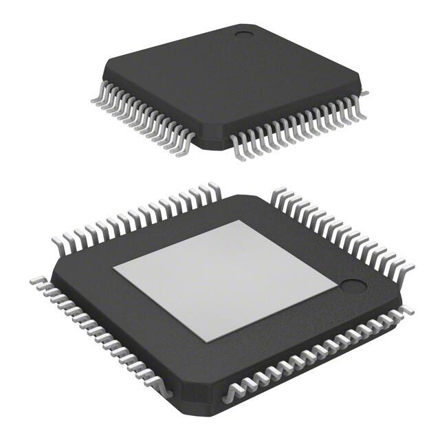
VSC8601
10/100/1000BASE-T PHY with RGMII
MAC Interface
Datasheet
VMDS-10210
Revision 4.1
September 2009
�Vitesse
Corporate Headquarters
741 Calle Plano
Camarillo, California 93012
United States
www.vitesse.com
Copyright© 2005–2007, 2009 by Vitesse Semiconductor Corporation
Vitesse Semiconductor Corporation (“Vitesse”) retains the right to make changes to its
products or specifications to improve performance, reliability or manufacturability. All
information in this document, including descriptions of features, functions,
performance, technical specifications and availability, is subject to change without
notice at any time. While the information furnished herein is held to be accurate and
reliable, no responsibility will be assumed by Vitesse for its use. Furthermore, the
information contained herein does not convey to the purchaser of microelectronic
devices any license under the patent right of any manufacturer.
Vitesse products are not intended for use in products or applications, including, but not
limited to, medical devices (including life support and implantable medical devices),
nuclear products, or other safety-critical uses where failure of a Vitesse product could
reasonably be expected to result in personal injury or death. Anyone using a Vitesse
product in such an application without express written consent of an officer of Vitesse
does so at their own risk, and agrees to fully indemnify Vitesse for any damages that
may result from such use or sale.
Safety of Laser Products, IEC 60825. While Vitesse products support IEC 60825, use of
Vitesse products does not ensure compliance to IEC 60825. Buyers are responsible for
ensuring compliance to IEC 60825. Buyers must fully indemnify Vitesse for any
damages resulting from non-compliance to IEC 60825.
Vitesse Semiconductor Corporation is a registered trademark. All other products or
service names used in this publication are for identification purposes only, and may be
trademarks or registered trademarks of their respective companies. All other
trademarks or registered trademarks mentioned herein are the property of their
respective holders.
Revision 4.1
September 2009
Page 2
�VSC8601 Datasheet
Contents
Contents
Revision History ..........................................................................................9
1
2
Introduction.....................................................................................13
Product Overview.............................................................................14
2.1
2.2
2.3
3
Functional Descriptions....................................................................17
3.1
3.2
3.3
3.4
3.5
3.6
3.7
3.8
3.9
3.10
3.11
3.12
3.13
4
Features ........................................................................................................... 14
Applications....................................................................................................... 15
Block Diagram ................................................................................................... 16
Interface and Media............................................................................................ 17
MAC Interface.................................................................................................... 17
3.2.1
MAC Resistor Calibration .......................................................................... 17
3.2.2
RGMII MAC Interface Mode ...................................................................... 17
Cat5 Media Interface .......................................................................................... 18
Cat5 Auto-Negotiation ........................................................................................ 19
Manual MDI/MDI-X Setting .................................................................................. 20
Automatic Crossover and Polarity Detection ........................................................... 20
Link Speed Downshift ......................................................................................... 21
Transformerless Ethernet..................................................................................... 21
Ethernet Inline Powered Devices .......................................................................... 21
ActiPHY Power Management................................................................................. 23
3.10.1 Low-Power State .................................................................................... 24
3.10.2 Link Partner Wake-Up State ..................................................................... 25
3.10.3 Normal Operating State ........................................................................... 25
Serial Management Interface ............................................................................... 25
3.11.1 SMI Frames ........................................................................................... 25
3.11.2 SMI Interrupts ....................................................................................... 27
LED Interface .................................................................................................... 28
3.12.1 Simple or Enhanced LED Method............................................................... 28
3.12.2 LED Modes............................................................................................. 28
3.12.3 LED Behavior ......................................................................................... 30
Testing Features................................................................................................. 30
3.13.1 Ethernet Packet Generator (EPG) .............................................................. 30
3.13.2 CRC Counters......................................................................................... 31
3.13.3 Far-end Loopback ................................................................................... 31
3.13.4 Near-End Loopback ................................................................................. 32
3.13.5 Connector Loopback................................................................................ 32
3.13.6 VeriPHY Cable Diagnostics........................................................................ 33
3.13.7 IEEE 1149.1 JTAG Boundary Scan ............................................................. 33
3.13.8 JTAG Instruction Codes............................................................................ 34
3.13.9 Boundary-Scan Register Cell Order............................................................ 36
Configuration ...................................................................................37
4.1
4.2
Registers........................................................................................................... 37
4.1.1
Reserved Registers ................................................................................. 38
4.1.2
Reserved Bits ......................................................................................... 38
IEEE Standard and Main Registers ........................................................................ 38
4.2.1
Mode Control ......................................................................................... 39
4.2.2
Mode Status........................................................................................... 40
Revision 4.1
September 2009
Page 3
�VSC8601 Datasheet
Contents
4.3
4.4
4.5
5
4.2.3
Device Identification ............................................................................... 41
4.2.4
Auto-Negotiation Advertisement ............................................................... 41
4.2.5
Link Partner Auto-Negotiation Capability .................................................... 42
4.2.6
Auto-Negotiation Expansion ..................................................................... 43
4.2.7
Transmit Auto-Negotiation Next Page......................................................... 43
4.2.8
Auto-Negotiation Link Partner Next Page Receive ........................................ 44
4.2.9
1000BASE-T Control................................................................................ 44
4.2.10 1000BASE-T Status................................................................................. 45
4.2.11 Main Registers Reserved Addresses ........................................................... 45
4.2.12 1000BASE-T Status Extension 1................................................................ 45
4.2.13 100BASE-TX Status Extension .................................................................. 46
4.2.14 1000BASE-T Status Extension 2................................................................ 46
4.2.15 Bypass Control ....................................................................................... 47
4.2.16 Receive Error Counter ............................................................................. 48
4.2.17 False Carrier Sense Counter ..................................................................... 48
4.2.18 Disconnect Counter................................................................................. 49
4.2.19 Extended Control and Status .................................................................... 49
4.2.20 Extended PHY Control Set 1 ..................................................................... 50
4.2.21 Extended PHY Control Set 2 ..................................................................... 50
4.2.22 Interrupt Mask ....................................................................................... 51
4.2.23 Interrupt Status ..................................................................................... 52
4.2.24 LED Control ........................................................................................... 52
4.2.25 Auxiliary Control and Status ..................................................................... 53
4.2.26 Delay Skew Status.................................................................................. 54
4.2.27 Reserved Address Space .......................................................................... 54
Extended Page Registers ..................................................................................... 55
4.3.1
Extended Page Access ............................................................................. 56
4.3.2
Enhanced LED Method Select ................................................................... 56
4.3.3
Enhanced LED Behavior ........................................................................... 57
4.3.4
CRC Good Counter .................................................................................. 58
4.3.5
MAC Resistor Calibration Control ............................................................... 58
4.3.6
Extended PHY Control 3........................................................................... 59
4.3.7
EEPROM Interface Status and Control ........................................................ 59
4.3.8
EEPROM Data Read/Write ........................................................................ 60
4.3.9
Extended PHY Control 4........................................................................... 60
4.3.10 Reserved Extended Registers ................................................................... 61
4.3.11 Extended PHY Control 5........................................................................... 61
4.3.12 RGMII Skew Control................................................................................ 62
4.3.13 Ethernet Packet Generator (EPG) Control 1 ................................................ 63
4.3.14 Ethernet Packet Generator Control 2 ......................................................... 64
CMODE ............................................................................................................. 64
4.4.1
CMODE Pins and Related Functions ........................................................... 64
4.4.2
Functions and Related CMODE Pins ........................................................... 65
4.4.3
CMODE Resistor Values............................................................................ 65
EEPROM............................................................................................................ 66
4.5.1
EEPROM Contents Description .................................................................. 66
4.5.2
Read/Write Access to the EEPROM ............................................................ 67
Electrical Specifications ...................................................................69
5.1
5.2
DC Characteristics .............................................................................................. 69
5.1.1
VDDIO at 3.3 V ...................................................................................... 69
5.1.2
VDDIO at 2.5 V ...................................................................................... 70
Current Consumption.......................................................................................... 70
5.2.1
Consumption with 1000BASE-T Link .......................................................... 70
5.2.2
Consumption with 100BASE-TX Link .......................................................... 71
Revision 4.1
September 2009
Page 4
�VSC8601 Datasheet
Contents
5.3
5.4
5.5
6
Pin Descriptions ...............................................................................84
6.1
6.2
6.3
6.4
7
Package Drawing................................................................................................ 93
Thermal Specifications ........................................................................................ 95
Moisture Sensitivity ............................................................................................ 95
Design Considerations .....................................................................96
8.1
8.2
8.3
8.4
8.5
8.6
8.7
8.8
8.9
8.10
9
Pin Diagram ...................................................................................................... 84
Pins by Function................................................................................................. 85
6.2.1
Twisted Pair Interface .............................................................................. 85
6.2.2
RGMII MAC Interface .............................................................................. 86
6.2.3
Serial Management Interface (SMI)........................................................... 87
6.2.4
JTAG ..................................................................................................... 88
6.2.5
Miscellaneous......................................................................................... 88
6.2.6
Power Supply ......................................................................................... 89
6.2.7
Power Supply and Associated Function....................................................... 90
Pins by Name .................................................................................................... 91
Pins by Number ................................................................................................. 92
Package Information........................................................................93
7.1
7.2
7.3
8
5.2.3
Consumption with 10BASE-T Link.............................................................. 72
5.2.4
Consumption with No Link and ActiPHY Enabled .......................................... 73
5.2.5
Consumption with No Link and ActiPHY Disabled ......................................... 73
5.2.6
Consumption in Power-Down Mode............................................................ 74
5.2.7
Consumption in Reset State ..................................................................... 75
AC Characteristics .............................................................................................. 75
5.3.1
Reference Clock Input ............................................................................. 76
5.3.2
Clock Output .......................................................................................... 76
5.3.3
JTAG Interface ....................................................................................... 77
5.3.4
SMI Interface ......................................................................................... 77
5.3.5
Device Reset .......................................................................................... 78
5.3.6
RGMII Uncompensated ............................................................................ 80
5.3.7
RGMII Compensated ............................................................................... 81
Operating Conditions .......................................................................................... 82
Stress Ratings ................................................................................................... 83
RX_CLK Can Reach as High as 55% Duty Cycle ...................................................... 96
First SMI Write Fails after Software Reset .............................................................. 96
Link-Up Issue In Forced 100BASE-TX Mode ............................................................ 96
Default 10Base-T Settings Are Marginal and Cause MAU Test Failure.......................... 97
On-Chip Pull-up Resistor Violation......................................................................... 99
Setting the Internal RGMII Timing Compensation Value ........................................... 99
10BASE-T Harmonics at 30 MHz and 50 MHz Marginally Violate Specification .............. 99
Voltage Overshoot When Using On-Chip Switching Regulator.................................. 100
Long Link-Up Times Caused by Noise on the Twisted Pair Interface ......................... 100
High VDD33 and Low VDDIOMAC Supply ............................................................. 101
Ordering Information .....................................................................102
Revision 4.1
September 2009
Page 5
�VSC8601 Datasheet
Contents
Figures
Figure
Figure
Figure
Figure
Figure
Figure
Figure
Figure
Figure
Figure
Figure
Figure
Figure
Figure
Figure
Figure
Figure
Figure
Figure
Figure
Figure
Figure
Figure
Figure
1.
2.
3.
4.
5.
6.
7.
8.
9.
10.
11.
12.
13.
14.
15.
16.
17.
18.
19.
20.
21.
22.
23.
24.
Revision 4.1
September 2009
Typical Application...................................................................................... 14
High-level Block Diagram ............................................................................ 16
RGMII to Cat5 Block Diagram ...................................................................... 17
RGMII MAC Interface .................................................................................. 18
Cat5 Media Interface .................................................................................. 19
Inline Powered Ethernet Switch Diagram ....................................................... 22
ActiPHY State ............................................................................................ 24
SMI Read Frame ........................................................................................ 26
SMI Write Frame........................................................................................ 26
MDINT Configured as an Open-Drain (Active-Low) Pin..................................... 27
MDINT Configured as an Open-Source (Active-High) Pin .................................. 27
Far-End Loopback ...................................................................................... 32
Near-End Loopback .................................................................................... 32
Connector Loopback ................................................................................... 32
Test Access Port and Boundary-Scan Architecture ........................................... 34
Register Space Diagram .............................................................................. 37
EEPROM Read and Write Register Flow .......................................................... 68
JTAG Interface Timing ................................................................................ 77
SMI Interface Timing .................................................................................. 78
Reset Timing ............................................................................................. 79
RGMII Uncompensated Timing ..................................................................... 81
RGMII Compensated Timing ........................................................................ 82
Pin Diagram .............................................................................................. 84
Package Drawing ....................................................................................... 94
Page 6
�VSC8601 Datasheet
Contents
Tables
Table
Table
Table
Table
Table
Table
Table
Table
Table
Table
Table
Table
Table
Table
Table
Table
Table
Table
Table
Table
Table
Table
Table
Table
Table
Table
Table
Table
Table
Table
Table
Table
Table
Table
Table
Table
Table
Table
Table
Table
Table
Table
Table
Table
Table
Table
Table
Table
Table
Table
Table
Table
Table
1.
2.
3.
4.
5.
6.
7.
8.
9.
10.
11.
12.
13.
14.
15.
16.
17.
18.
19.
20.
21.
22.
23.
24.
25.
26.
27.
28.
29.
30.
31.
32.
33.
34.
35.
36.
37.
38.
39.
40.
41.
42.
43.
44.
45.
46.
47.
48.
49.
50.
51.
52.
53.
Interface and Media ................................................................................... 17
Supported MDI Pair Combinations ................................................................ 21
LED Mode and Function Summary ................................................................ 28
JTAG Device Identification Register Description .............................................. 35
JTAG Interface Instruction Codes ................................................................. 35
IEEE 802.3 Standard Registers .................................................................... 38
Main Registers ........................................................................................... 38
Mode Control, Address 0 (0x00)................................................................... 39
Mode Status, Address 1 (0x01) .................................................................... 40
Identifier 1, Address 2 (0x02)...................................................................... 41
Identifier 2, Address 3 (0x03)...................................................................... 41
Device Auto-Negotiation Advertisement, Address 4 (0x04) .............................. 41
Auto-Negotiation Link Partner Ability, Address 5 (0x05)................................... 42
Auto-Negotiation Expansion, Address 6 (0x06)............................................... 43
Auto-Negotiation Next Page Transmit, Address 7 (0x07) .................................. 43
Auto-Negotiation LP Next Page Receive, Address 8 (0x08) ............................... 44
1000BASE-T Control, Address 9 (0x09) ......................................................... 44
1000BASE-T Status, Address 10 (0x0A) ........................................................ 45
1000BASE-T Status Extension 1, Address 15 (0x0F) ....................................... 45
100BASE-TX Status Extension, Address 16 (0x10) .......................................... 46
1000BASE-T Status Extension 2, Address 17 (0x11) ....................................... 46
Bypass Control, Address 18 (0x12)............................................................... 47
Receive Error Counter, Address 19 (0x13) ..................................................... 48
False Carrier Sense Counter, Address 20 (0x14) ............................................. 48
Disconnect Counter, Address 21 (0x15)......................................................... 49
Extended Control and Status, Address 22 (0x16) ........................................... 49
Extended PHY Control 1, Address 23 (0x17) .................................................. 50
Extended PHY Control 2, Address 24 (0x18) .................................................. 50
Interrupt Mask, Address 25 (0x19)............................................................... 51
Interrupt Status, Address 26 (0x1A)............................................................. 52
LED Control, Address 27 (0x1B)................................................................... 52
Auxiliary Control and Status, Address 28 (0x1C) ............................................ 53
Delay Skew Status, Address = 29 (0x1D)...................................................... 54
Extended Registers Page Space.................................................................... 55
Extended Page Access, Address 31 (0x1F)..................................................... 56
Enhanced LED Method Select, Address 16E (0x10) ......................................... 56
Available LED Mode Settings........................................................................ 56
Enhanced LED Behavior, Address 17E (0x11) ................................................. 57
CRC Good Counter, Address 18E (0x12) ........................................................ 58
MAC Resistor Calibration Control, Address 19E (0x13)..................................... 58
Extended PHY Control 3, Address 20E (0x14)................................................. 59
EEPROM Interface Status and Control, Address 21E (0x15).............................. 59
EEPROM Read or Write, Address 22E (0x16) .................................................. 60
Extended PHY Control 4, Address 23E (0x17)................................................. 60
Extended PHY Control 5, Address 27E (0x1B) ................................................ 61
RGMII Skew Control, Address 28E (0x1C) ..................................................... 62
EPG Control Register 1, Address 29E (0x1D).................................................. 63
EPG Control Register 2, Address 30E (0x1E) .................................................. 64
CMODE Configuration Pins and Device Functions ............................................ 64
Device Functions and Associated CMODE Pins ................................................ 65
CMODE Resistor Values and Resultant Bit Settings .......................................... 65
EEPROM Configuration Contents................................................................... 67
DC Characteristics for VDD33, VDDIOMAC, or VDDIOMICRO at 3.3 V ................ 69
Revision 4.1
September 2009
Page 7
�VSC8601 Datasheet
Contents
Table
Table
Table
Table
Table
Table
Table
Table
Table
Table
Table
Table
Table
Table
Table
Table
Table
Table
Table
Table
Table
Table
Table
Table
Table
Table
Table
Table
Table
Table
Table
Table
Table
Table
54.
55.
56.
57.
58.
59.
60.
61.
62.
63.
64.
65.
66.
67.
68.
69.
70.
71.
72.
73.
74.
75.
76.
77.
78.
79.
80.
81.
82.
83.
84.
85.
86.
87.
DC Characteristics for VDDIOMAC or VDDIOMICRO at 2.5 V............................. 70
Current Consumption: 1000BASE-T, Regulator Enabled ................................... 70
Current Consumption: 1000BASE-T, Regulator Disabled................................... 71
Current Consumption: 100BASE-TX, Regulator Enabled ................................... 71
Current Consumption: 100BASE-TX, Regulator Disabled .................................. 71
Current Consumption: 10BASE-T, Regulator Enabled ....................................... 72
Current Consumption: 10BASE-T, Regulator Disabled ...................................... 72
Current Consumption: No Link, ActiPHY Enabled, Regulator Enabled ................. 73
Current Consumption: No Link, ActiPHY Enabled, Regulator Disabled ................ 73
Current Consumption: No Link, ActiPHY Disabled, Regulator Enabled ................ 73
Current Consumption: No Link, ActiPHY Disabled, Regulator Disabled................ 74
Current Consumption: Power-Down, Regulator Enabled................................... 74
Current Consumption: Power-Down, Regulator Disabled .................................. 75
Current Consumption: Reset State ............................................................... 75
AC Characteristics for REFCLK Input ............................................................. 76
AC Characteristics for REFCLK Input with 25 MHz Clock Input .......................... 76
AC Characteristics for the CLKOUT Pin .......................................................... 76
AC Characteristics for the JTAG Interface....................................................... 77
AC Characteristics for the SMI Interface ........................................................ 77
AC Characteristics for Device Reset .............................................................. 78
AC Characteristics for RGMII Uncompensated ................................................ 80
AC Characteristics for RGMII Compensated.................................................... 81
Recommended Operating Conditions............................................................. 82
Stress Ratings ........................................................................................... 83
Pin Type Symbols ....................................................................................... 85
Twisted Pair Interface Pins........................................................................... 85
RGMII MAC Interface Pins ........................................................................... 86
SMI Pins ................................................................................................... 87
JTAG Pins.................................................................................................. 88
Miscellaneous Pins ..................................................................................... 88
Power Supply Pins...................................................................................... 89
Power Supply Pins and Associated Function Pins............................................. 90
Thermal Resistances................................................................................... 95
Ordering Information................................................................................ 102
Revision 4.1
September 2009
Page 8
�VSC8601 Datasheet
Revision History
Revision History
This section describes the changes that were implemented in this document. The
changes are listed by revision, starting with the most current publication.
Revision 4.1
Revision 4.1 of this datasheet was published in September 2009. In revision 4.1 of the
document, design considerations were added. For more information, see “Design
Considerations,” page 96.
Revision 4.0
Revision 4.0 of this datasheet was published in November 2007. The following is a
summary of the changes implemented in the datasheet:
•
The VSC8601KN package was removed. VSC8601XKN remains available.
•
The electrostatic discharge voltage values were added. For charged device model, it
is ±500. For human body model, it is ±1500.
•
The moisture sensitivity is now specified as level 3.
•
In the jumbo packet register settings (28E.11:10), the packet lengths were
updated.
•
In several current consumption specifications, the values for total power at 2.5 V
were corrected. The previous values were slightly elevated.
•
In the DC characteristics for VDDIO at 3.3 V, both the input and output leakage
current parameters (IILEAK and IOLEAK) were increased from ±36 µA to ±43 µA.
•
In the DC characteristics for VDDIO at 2.5 V, the minimum input high voltage (VIH)
was increased from 1.7 V to 2.0 V. Both the input and output leakage current
parameters (IILEAK and IOLEAK) were increased from ±25 µA to ±35 µA.
•
Current consumption specifications were added for both the power-down mode and
the reset state.
•
In the AC characteristics for the CLKOUT pin, the duty cycle (%DUTY) was modified
from 40% minimum to 44% minimum and from 60% maximum to 56% maximum.
Also, the total jitter (JCLK) was raised from 491 ps maximum to 600 ps maximum,
with the qualifier “time interval error” added to the condition.
•
In the SMI specifications, the MDC rise and fall times were corrected from minimum
values to maximum values.
•
For the device reset rise time specification, a condition was added that it is
measured from a 10% level to a 90% level.
•
In the AC characteristics for RGMII uncompensated, the 1000BASE-T duty cycle
(tDUTY1000) was separated into two sets of values. In the first set, the values remain
the same, but the added condition is: at room temperature and nominal supply and
Revision 4.1
September 2009
Page 9
�VSC8601 Datasheet
Revision History
register 28E.13:12 set to 10 or 11. In the second set, the minimum is 40% and the
maximum is 60% and the condition is: register 28E.13:12 set to 00 or 01.
•
In the AC characteristics for RGMII compensated, all of the setup and hold times
were modified from 0 ns maximum to 3 ns maximum.
•
In the description of pin MDIO, the type was corrected from open drain (OD) to
input and output (I/O).
•
The PLLMODE pin description was updated with additional clocking information. If a
crystal or an external 25 MHz clock is used, PLLMODE must be pulled low. If an
external 125 MHz clock is used, PLLMODE must be pulled high.
•
A design guideline was added regarding writes from the serial management
interface (SMI) after a software reset.
•
A design guideline was added regarding delays in the link-up process while in the
forced 100BASE-TX mode with the automatic MDI/MDI-X detection feature enabled.
•
The following design guidelines were removed, because they no longer apply to the
device: Remote Fault Status; DSP Optimization Script Required; Default Port Type
Incorrect; and Core 1.2 V Supply Needs to Meet Specific Range.
Revision 2.2
Revision 2.2 of this datasheet was published in July 2006. The following is a summary
of the changes implemented in the datasheet:
•
In the inline powered Ethernet switch diagram, a reference to “SGMII interface”
was corrected to “RGMII interface.”
•
In the description of CRC counters, the CRC good counter’s highest value was
corrected from 10,000 to 9,999 packets, after which the counter clears.
•
The device revision number definition was updated from 0000 to 0001 in the
identifier 2 register (address 3) and the JTAG device identification.
•
In the DC Characteristics for VDD33, VDDIOMAC, or VDDIOMICRO at 3.3 V, the output
leakage (IOLEAK) was changed to match the same values as the input leakage
(IILEAK) with the same condition (internal resistor included). Specifically, the values
were changed from –10 µA minimum and 10 µA maximum to –36 µA minimum and
36 µA maximum.
•
In the DC Characteristics for VDDIOMAC or VDDIOMICRO at 2.5 V, the output leakage
(IOLEAK) was changed to match the same values as the input leakage (IILEAK) with
the same condition (internal resistor included). Specifically, the values were
changed from –10 µA minimum and 10 µA maximum to –25 µA minimum and
25 µA maximum.
•
In the DC characteristics for VDDIOMAC or VDDIOMICRO at 2.5 V, the output high
voltage parameter (VOH) incorrectly stated IOH = 1.0 mA as a condition. It is now
corrected to the condition IOH = –1.0 mA.
•
For all the current consumption specifications with the on-chip switching regulator
enabled, the specification values for IVDD12 and IVDD12A were removed because
Revision 4.1
September 2009
Page 10
�VSC8601 Datasheet
Revision History
they were inadvertently added in a prior revision of this document. The IVDD12 and
IVDD12A values are kept for current consumption with the regulator disabled.
•
For the 100BASE current consumption specifications, all references to the speed
were corrected from 100BASE-X to 100BASE-TX.
•
In the AC characteristics for the CLKOUT pin, the total jitter specifications were
added. They are 217 ps typical and 491 ps maximum.
•
For device reset, both the reset characteristics and timing diagram were updated to
include new parameters: reset rise time (tRST_RISE) and supply stable time
(tVDDSTABLE).
•
In the stress ratings, the power supply voltage parameter was removed because it
was redundant.
•
In the pin description for TX_CLK, the rate was clarified to be 2.5 MHz for 10 Mbps
mode, 25 MHz for 100 Mbps mode, or 125 MHz for 1000 Mbps mode.
•
The errata item “RX_CLK Can Reach as High as 55% Duty Cycle” remains in effect
but all other errata items no longer apply to the latest part revision.
Revision 2.1
Revision 2.1 of this datasheet was published in February 2006. The following is a
summary of the changes implemented in the datasheet:
•
In the high-level block diagram, representation of the XTAL pin was corrected from
“XTAL 1/2” to “XTAL1” and “XTAL2.”
•
In the RGMII to Cat5 block diagram, the interface name was corrected from GMII to
RGMII.
•
New information was added about how to manually force the device to use
MDI/MDI-X.
•
The VSC8601 device switches between the low-power state and LP wake-up state
every two seconds; the rate is not programmable, as was originally stated.
•
In the link partner wake-up state, the device sends FLP bursts for two seconds;
they are not limited to three bursts, as was originally stated.
•
In the description of the PHY address for the serial management interface (SMI),
the physical address was corrected from 3:0 to 4:0.
•
For the enhanced LED method, controlled by MII Register 16E, two of the LED
modes have changed. Mode 11, TX activity, and mode 13, RX activity, are now both
reserved.
•
In the description of the far-end loopback testing feature, the controlling register
bit was corrected from 23.3 to 27E.10.
•
For the JTAG interface instructions EXTEST and SAMPLE/PRELOAD, the values for
register width were modified from TBD to 45.
•
For the Mode Control register (address 0), when bit 11 (power-down) is set, RGMII
in-band signaling will not function.
Revision 4.1
September 2009
Page 11
�VSC8601 Datasheet
Revision History
•
In the Identifier 2 register (address 3), which enables device identification, the
default for bits 9:4 was modified from TBD to 000010.
•
In the LED Control register (address 27), the name for bits 2 and 1 was corrected
from “link/activity” to simply “activity.”
•
In the ActiPHY Control (address 20E), bit 5 was reassigned from being reserved to
being the MAC RX_CLK disable parameter.
•
In the extended PHY control 4 register (address 23E), all the bit settings were
mistakenly omitted. They are now restored.
•
In the Extended PHY Control 5 register (address 27E), the settings have changed
for bits 8:6 and 5:3 (100BASE-TX and 1000BASE-T transmitter amplitude control).
For bits 8:6 (100BASE-TX), the setting 011 changed from +5 amplitude to
reserved, making bit setting 010 (+4 amplitude) the largest. For bits 5:3
(1000BASE-T), the setting 011 changed from +3 amplitude to reserved, making bit
setting 010 (+2 amplitude) the largest.
•
For added clarity, the table that lists device functions and related CMODE pins now
references the associated register and bit for each function.
•
For the EEPROM Configuration Contents table, some address locations were added
and the introductory text was corrected.
•
For the DC electrical specifications with VDDIO at 3.3 V and with VDDIO at 2.5 V, an
additional condition was added. The specifications may be considered valid only
when VDDREG = 3.3 V.
•
The current consumption specifications were replaced with a new set of
specifications.
•
In the recommended operating conditions, the minimum and maximum values
were modified for the VDDIOMICRO, VDDIOMAC, and VDD33 parameters at 3.3 V.
For all of these parameters, the minimum changed from 3.13 V to 3.0 V and the
maximum changed from 3.47 V to 3.6 V. The VDDREG parameter was added to the
recommended operating conditions.
•
In the stress ratings, a new rating was added for the VDDREG parameter.
•
An errata section was added.
Revision 2.0
Revision 2.0 of this datasheet was published in December 2005. This was the first
publication of the document.
Revision 4.1
September 2009
Page 12
�VSC8601 Datasheet
Introduction
1
Introduction
This document consists of descriptions and specifications for both functional and
physical aspects of the VSC8601 10/100/1000BASE-T PHY with RGMII MAC Interface.
In addition to the datasheet, Vitesse maintains an extensive device-specific library of
support and collateral materials that you may find useful in developing your own
product. Depending upon the Vitesse device, this library may include:
•
Software Development Kits with sample commands and scripts
•
Reference designs showing the Vitesse device built in to applications in ways
intended to exploit its relative strengths
•
Presentations highlighting the operational features and specifications of the device
to assist in developing your own product road map
•
Input/Output Buffer Information specification (IBIS) models to help you create and
support the interfaces available on the particular Vitesse product
•
Application notes that provide detailed descriptions of the use of the particular
Vitesse product to solve real-world problems
•
White papers published by industry experts that provide ancillary and background
information useful in developing products that take full advantage of Vitesse
product designs and capabilities
•
User guides that describe specific techniques for interfacing to the particular Vitesse
products
Visit and register as a user on the Vitesse Web site to keep abreast of the latest
innovations from research and development teams and the most current product and
application documentation. The address of the Vitesse Web site is www.vitesse.com.
Revision 4.1
September 2009
Page 13
�VSC8601 Datasheet
Product Overview
2
Product Overview
The VSC8601 device is a low-power Gigabit Ethernet (GbE) transceiver ideal for Gigabit
LAN-on-Motherboard applications. The device’s compact, plastic low-profile quad flat
package (LQFP) with an exposed pad is optimal for footprint-sensitive applications.
Vitesse’s mixed signal and digital signal processing (DSP) architecture assures robust
performance. It supports both half-duplex and full-duplex 10BASE-T, 100BASE-TX, and
1000BASE-T communication speeds over Category 5 (Cat5) unshielded twisted pair
(UTP) cable at distances greater than 140 m, displaying excellent tolerance to NEXT,
FEXT, echo, and other types of ambient environment and system electronic noise.
The following illustration shows a high-level, generic view of a VSC8601 application.
Figure 1.
Typical Application
3.3 V
10/100/1000BASE-T MAC,
Switching ASIC,
or Network Processor
RGMII
VSC8601
10/100/1000BASE-T
Transceiver
Management I/F (MDC / MDIO)
2.1
RJ45+Magnetics
25 MHz
Features
This section lists key aspects of the VSC8601 device functionality and design that
distinguish it from similar products:
•
10/100/1000BASE-T PHY with industry’s lowest power consumption.
•
Compliant with IEEE 802.3 (10BASE-T, 100BASE-TX, 1000BASE-T) specifications.
•
Supports RGMII versions 1.3 and 2.0 (2.5 V, 3.3 V) MAC interface.
•
Low EMI line driver with integrated line side termination resistors.
•
Up to 16 kB jumbo frame support in all speeds.
•
Three programmable direct drive LEDs.
•
Suite of test modes, including loopback paths, Ethernet packet generators, and CRC
counters.
•
The VeriPHY® suite provides extensive network cable information such as cable
length, termination status, and open/short fault location.
•
ActiPHYTM power saving modes.
•
Advanced power management complies with Wake-on-LANTM and PCI2.2 power
requirements.
Revision 4.1
September 2009
Page 14
�VSC8601 Datasheet
Product Overview
2.2
•
Legacy Power-over-Ethernet (POE) support.
•
Powered by a single 3.3 V supply by using the optional on-chip switching regulator.
•
IEEE 1149.1 JTAG boundary-scan support.
•
10 mm × 10 mm, 64-pin, plastic LQFP package with an exposed pad.
Applications
Suggested applications for the VSC8601 device include:
•
LAN-on-Motherboards, NICs, and mobile PCs
•
iSCSI and TOE applications
•
Workgroup and desktop switches and routers
•
Gigabit Ethernet SAN, NAS, and MAN systems
•
Network-enabled devices such as printers, IP phones, and gaming appliances
•
ATCATM 3.0 and PICMGTM 2.16 Ethernet backplane applications
Revision 4.1
September 2009
Page 15
�VSC8601 Datasheet
Product Overview
2.3
Block Diagram
The following illustration shows the primary functional blocks of the VSC8601 device.
Figure 2.
High-level Block Diagram
TXVPA
TXVNA
TX_CLK
TXD[3:0]
TX_CTL
RX_CLK
RGMII MAC
Interface
Jumbo Packet
FIFO
10/100/
1000BASE-T
PCS
10/100/
1000BASE-T
PMA
MDI
Twisted Pair
Interface
RXD[3:0]
MDI Reference
CMODE[3:0]
NRESET
MDC
MDIO
MDINT
JTAG
Management
and Control
Interface
LED Interface
LED[2:0]
REG_EN
REG_OUT
NTRST
TMS
TCK
TDO
TDI
REF_REXT
XTAL1
XTAL2
CLKOUT
Power Regulation
EECLK
REF_FILT
PLL
EEDAT
Revision 4.1
September 2009
TXVPC
TXVNC
TXVPD
TXVND
RX_CTL
NSRESET
TXVPB
TXVNB
Page 16
�VSC8601 Datasheet
Functional Descriptions
3
Functional Descriptions
This section provides detailed information about how the VSC8601 device works, what
configurations and operational features are available, and how to test its functions. It
includes descriptions of the various device interfaces and how to set them up.
3.1
Interface and Media
The VSC8601 device operates with the interface and media shown in the following table
and illustration.
Table 1.
Interface and Media
Operating Mode
MAC Interface
RGMII - Cat5
Figure 3.
10/100/1000BASE-T
RGMII to Cat5 Block Diagram
MAC
3.2
Supported Media
RGMII
RGMII
VSC8601
Cat5
Cat5
Link Partner
MAC Interface
The VSC8601 supports RGMII versions 1.3 and 2.0 (2.5 V, 3.3 V) MAC interface.
3.2.1
MAC Resistor Calibration
To simplify board design, the VSC8601 MAC interface uses SimpliPINTM outputs that can
self-calibrate to a desired impedance characteristic to eliminate the need for series
termination resistors. By default, these RX output pins calibrate to 50 Ω. In addition,
MII Register 19E, bits 15:14 can be used to select different target impedances. For
more information, see “MAC Resistor Calibration Control,” page 58.
3.2.2
RGMII MAC Interface Mode
The RGMII interface can support all three speeds (10 Mbps, 100 Mbps, and 1000 Mbps)
and is used as an interface to an RGMII-compatible MAC.
Revision 4.1
September 2009
Page 17
�VSC8601 Datasheet
Functional Descriptions
Figure 4.
RGMII MAC Interface
SimpliPHY
RGMII MAC
RT
RT
TXD[3]
TXD[1]
TD [ 0 ]
RT
RT
TXC
RT
T X _C T L
RT
TD [ 3 ]
TD [ 2 ]
TD [ 1 ]
RD [ 3 ]
RD [ 2 ]
RD [ 1 ]
RD [ 0 ]
RX C
R X _C T L
3.3
TXD[2]
TXD[0]
TX_CLK
TX_CTL
50
50
50
50
50
50
RXD[3]
RXD[2]
RXD[1]
RXD[0]
RX_CLK
RX_CTL
Cat5 Media Interface
The twisted pair interface on the VSC8601 is compliant with the IEEE802.3-2000
specifications for Cat5 media. The VSC8601, unlike other Gigabit PHYs, has all passive
components (required to connect the PHY’s Cat5 interface to an external 1:1
transformer) fully integrated into the device. The connection of the twisted pair
interface is shown in the following figure.
Revision 4.1
September 2009
Page 18
�VSC8601 Datasheet
Functional Descriptions
Figure 5.
Cat5 Media Interface
SimpliPHY
TXVP_A_n
Transformer
0.1 µF
RJ-45
1 A+
2 A-
TXVN_A_n
TXVP_B_n
0.1 µF
3
B+
6
B-
TXVN_B_n
TXVP_C_n
4
C+
5
C-
0.1 µF
TXVN_C_n
7
D+
8
D-
TXVP_D_n
0.1 µF
TXVN_D_n
75
75
1000pF, 2kV
75
75
3.4
Cat5 Auto-Negotiation
The VSC8601 device supports twisted pair auto-negotiation as defined by clause 28 of
the IEEE standard 802.3-2000.
The auto-negotiation process consists of the evaluation of the advertised capabilities of
the PHY and its link partner to determine the best possible operating mode, throughput
speed, duplex configuration, and master or slave operating modes in the case of
1000BASE-T setups. Auto-negotiation also allows a connected MAC to communicate
with its link partner MAC through the VSC8601 device using the optional “next pages,”
which set attributes that may not otherwise be defined by the IEEE standard.
In installations where the Cat5 link partner does not support auto-negotiation, the
VSC8601 automatically switches to use parallel detection to select the appropriate link
speed.
Clearing VSC8601 device register 0, bit 12 disables clause 28 twisted-pair
auto-negotiation. If auto-negotiation is disabled, the state of register bits 0.6, 0.13,
Revision 4.1
September 2009
Page 19
�VSC8601 Datasheet
Functional Descriptions
and 0.8 determine the device operating speed and duplex mode. For more information
about configuring auto-negotiation, see “IEEE Standard and Main Registers,” page 38.
3.5
Manual MDI/MDI-X Setting
As an alternative to automatic MDI/MDI-X detection (using HP Auto-MDIX technology),
you can force the PHY to select MDI or MDI-X using the following scripts.
Format:
Phywrite ( register(dec), data(hex) )
Phywritemask ( register(dec), data(hex), mask(hex) )
To force MDI:
Phywrite ( 31, 0x2A30 )
Phywritemask ( 5, 0x0010, 0x0018 )
Phywrite ( 31, 0x0000 )
To force MDI-X:
Phywrite ( 31, 0x2A30 )
Phywritemask ( 5, 0x0018, 0x0018 )
Phywrite ( 31, 0x0000 )
To resume MDI/MDI-X setting based on register 18, bits 7 and 5:
Phywrite ( 31, 0x2A30 )
Phywritemask ( 5, 0x0000, 0x0018 )
Phywrite ( 31, 0x0000 )
3.6
Automatic Crossover and Polarity Detection
For trouble-free configuration and management of Ethernet links, the VSC8601 device
includes a robust, automatic, media-dependent and crossed media-dependent
detection feature, HP Auto-MDIX, in all of its three available speeds (10BASE-T,
100BASE-T, and 1000BASE-T). The function is fully compliant with clause 40 of the IEEE
standard 802.3-2002.
Additionally, the device detects and corrects polarity errors on all MDI pairs—a useful
capability that exceeds the requirements of the standard.
Both HP Auto-MDIX detection and polarity correction are enabled in the device by
default. The default settings are adjustable using device register bits 18.5:4. Status
bits for each of these functions are located in register 28.
Revision 4.1
September 2009
Page 20
�VSC8601 Datasheet
Functional Descriptions
The VSC8601 device’s algorithm for HP Auto-MDIX successfully detects, corrects, and
operates with any of the MDI wiring pair combinations listed in the following table.
Table 2.
Supported MDI Pair Combinations
RJ-45 Pin Pairings
1, 2
3, 6
4, 5
7, 8
A
B
C
D
Mode
Normal MDI
B
A
D
C
Normal MDI-X
A
B
D
C
Normal MDI with pair swap on C and D pair
B
A
C
D
Normal MDI-X with pair swap on C and D pair
Note The VSC8601 device can be configured to perform HP Auto-MDIX even when its
auto-negotiation feature is disabled (setting register 0.12 to 0) and the link is forced
into 10/100 speeds. To enable this feature, set register 27E.15 = 0.
3.7
Link Speed Downshift
For operation in cabling environments that are incompatible with 1000BASE-T, the
VSC8601 device provides an automatic link speed “downshift” option. When enabled,
the device automatically changes its 1000BASE-T auto-negotiation advertisement to
the next slower speed after a set number of failed attempts at 1000BASE-T.
This is useful in networks using older cable installations that may include only pairs A
and B and not pairs C and D.
To configure and monitor link speed downshifting, use register bits 20E.4:1. For more
information, see “Extended PHY Control Set 1,” page 50.
3.8
Transformerless Ethernet
The Cat5 media interface supports 10/100/1000BT Ethernet for backplane applications
such as those specified by the PICMGTM 2.16 and ATCATM 3.0 specifications for
eight-pin channels. With proper AC coupling, the typical Cat5 transformer can be
removed and replaced with capacitors.
3.9
Ethernet Inline Powered Devices
The VSC8601 device can detect inline powered devices in Ethernet network
applications. Its inline powered detection capability can be part of a system that allows
for IP-phone and other devices, such as wireless access points, to receive power
directly from their Ethernet cable, similar to office digital phones receiving power from
a Private Branch Exchange (PBX) office switch over the telephone cabling. This can
eliminate the need for an IP-phone to have an external power supply. It also enables
the inline powered device to remain active during a power outage (assuming the
Ethernet switch is connected to an uninterrupted power supply, battery, back-up power
generator, or some other uninterruptible power source).
For more information about inline powered device detection, visit the Cisco Web site at
www.cisco.com.
Revision 4.1
September 2009
Page 21
�VSC8601 Datasheet
Functional Descriptions
The VSC8601 device is compatible with switch designs that are intended for use in
systems that supply power to Data Terminal Equipment (DTE) using the MDI or twisted
pair cable, as described in clause 33 of the IEEE standard 802.3af. The following
illustration shows an example of this type of application.
Figure 6.
Inline Powered Ethernet Switch Diagram
Gigabit Switch
RGMII
Interface
Processor
Control
SMI
PHY_0
PHY_1
PHY_n
Inline
Power
Supply Unit
X-former
X-former
X-former
RJ-45
I/F
RJ-45
I/F
RJ-45
I/F
Cat5
The following procedure describes the process that an Ethernet switch must perform to
process inline power requests made by a link partner (LP) that is, in turn, capable of
receiving inline power.
1.
Enable the inline powered device detection mode on each VSC8601 PHY using its
serial management interface. Set register bit 23E.10 to 1.
2.
Ensure that the VSC8601 device auto-negotiation enable bit (register 0.12) is also
set to 1. In the application, the device sends a special Fast Link Pulse (FLP) signal
to the LP. Reading register bit 23E.9:8 returns 00 during the search for devices that
require Power-over-Ethernet (PoE).
3.
The VSC8601 PHY monitors its inputs for the FLP signal looped back by the LP. An
LP capable of receiving PoE will loopback the FLP pulses when it is in a
powered-down state. This is reported when VSC8601 device register bit 23E.9:8
reads back 01. It can also be verified as an inline power detection interrupt by
Revision 4.1
September 2009
Page 22
�VSC8601 Datasheet
Functional Descriptions
reading VSC8601 device register bit 26.9, which should be a 1, and which is
subsequently cleared and the interrupt de-asserted after the read.
If an LP device does not loop back the FLP after a specific time, VSC8601 device
register bit 23E.9:8 automatically resets to 10.
3.10
4.
If the VSC8601 PHY reports that the LP needs PoE, the Ethernet switch must enable
inline power on this port, externally of the PHY.
5.
The PHY automatically disables inline powered device detection if the VSC8601
device register bit 23E.9:8 automatically resets to 10, and then automatically
changes to its normal auto-negotiation process. A link is then auto-negotiated and
established when the link status bit is set (register bit 1.2 is set to 1).
6.
In the event of a link failure (indicated when VSC8601 device register bit 1.2 reads
0), the inline power should be disabled to the inline powered device external to the
PHY. The VSC8601 PHY disables its normal auto-negotiation process and re-enables
its inline powered device detection mode.
ActiPHY Power Management
In addition to the IEEE-specified power-down control bit (device register bit 0.11), the
device also includes an ActiPHY™ power management mode for each PHY. This mode
enables support for power-sensitive applications such as laptop computers with
Wake-on-LAN™ capability. It utilizes a signal-detect function that monitors the media
interface for the presence of a link to determine when to automatically power-down the
PHY. The PHY “wakes up” at a programmable interval and attempts to “wake up” the
link partner PHY by sending a burst of FLP over copper media.
The ActiPHY power management mode in the VSC8601 device can be enabled during
normal operation at any time by setting register bit 23.5 to 1.
There are three operating states possible when ActiPHY mode is enabled:
•
Low-power state
•
LP wake-up state
•
Normal operating state (link-up state)
The VSC8601 device switches between the low-power state and LP wake-up state every
two seconds until signal energy is detected on the media interface pins. When signal
energy is detected, the PHY enters the normal operating state. If the PHY is in its
normal operating state and the link fails, the PHY returns to the low-power state after
the link status time-out timer has expired. After reset, the PHY enters the low-power
state.
When auto-negotiation is enabled in the PHY, the ActiPHY state machine operates as
described. If auto-negotiation is disabled and the link is forced to 10BT or 100BTX
modes while the PHY is in its low-power state, the PHY continues to transition between
the low-power and LP wake-up states until signal energy is detected on the media pins.
At that time, the PHY transitions to the normal operating state and stays in that state
even when the link is dropped. If auto-negotiation is disabled while the PHY is in the
normal operation state, the PHY stays in that state when the link is dropped and does
not transition back to the low-power state.
Revision 4.1
September 2009
Page 23
�VSC8601 Datasheet
Functional Descriptions
The following illustration shows the relationship between ActiPHY states and timers.
Figure 7.
ActiPHY State
Low-Power State
Signal Energy Detected on
Media
FLP Burst
Signal Sent
Sleep Timer Expires
Timeout Timer Expires and
Auto-Negotiation Enabled
LP Wake-up
State
3.10.1
Normal
Operation
Low-Power State
In the low-power state, all major digital blocks are powered down. However, the
following functionality is provided:
•
SMI interface (MDC, MDIO, MDINT)
•
CLKOUT
In this state, the PHY monitors the media interface pins for signal energy. The PHY
comes out of low-power state and transitions to the normal operating state when signal
energy is detected on the media. This happens when the PHY is connected to one of the
following:
•
Auto-negotiation capable link partner
•
Auto-negotiation incapable (blink/forced) link partner (100BASE-TX or 10BASE-T)
•
Another PHY in ActiPHY LP wake-up state
In the absence of signal energy on the media pins, the PHY transitions from the
low-power state to the LP wake-up state periodically based on the programmable sleep
timer (register bits 20E.14:13). The actual sleep time duration is randomized from
–80 ms to +60 ms to avoid two linked PHYs in ActiPHY Mode entering a lock-up state
during operation.
Revision 4.1
September 2009
Page 24
�VSC8601 Datasheet
Functional Descriptions
3.10.2
Link Partner Wake-Up State
In this state, the PHY attempts to wake up the link partner. FLP bursts are sent on
alternating pairs A and B of the Cat5 media for a duration of two seconds.
In this state, the following functionality is provided:
•
SMI interface (MDC, MDIO, MDINT)
•
CLKOUT
After sending signal energy on the relevant media, the PHY returns to the low-power
state.
3.10.3
Normal Operating State
In this state, the PHY establishes a link with a link partner. When the media is
unplugged or the link partner is powered down, the PHY waits for the duration of the
programmable link status time-out timer, which is set using register bit 28.7 and
bit 28.2. It then enters the low-power state.
3.11
Serial Management Interface
The VSC8601 device includes an IEEE 802.3-compliant serial management interface
(SMI) that is affected by use of its MDC and MDIO pins. The SMI provides access to
device control and status registers. The register set that controls the SMI consists of 32
16-bit registers, including all required IEEE-specified registers. Also, there are
additional pages of registers accessible by means of device register 31.
For more information, see “Extended Page Registers,” page 55.
The SMI is a synchronous serial interface with bidirectional data on the MDIO pin that is
clocked on the rising edge of the MDC pin. The interface can be clocked at a rate from
0 MHz to 25 MHz, depending upon the total load on MDIO. An external, 2 kΩ pull-up
resistor is required on the MDIO pin.
3.11.1
SMI Frames
Data is transferred over the SMI using 32-bit frames with an optional and arbitrary
length preamble. The following illustrations show the SMI frame format for the read
operation and write operation.
Revision 4.1
September 2009
Page 25
�VSC8601 Datasheet
Functional Descriptions
Figure 8.
SMI Read Frame
Station Manager Drives MDIO
PHY Drives MDIO
MDC
MDIO
Z
Z
1
0
1
1
Preamble SFD
(optional)
Idle
Figure 9.
0
A4
Read
A3
A2
A1
A0
PHY Address
R4 R3 R2 R1 R0
Z
Register Address
to PHY
0
TA
D15 D14 D13 D12 D11 D10 D9 D8 D7 D6 D5 D4 D3 D2 D1 D0
Z
Register Data from PHY
Z
Idle
SMI Write Frame
Station Manager Drives MDIO (PHY tristates MDIO during entire sequence)
MDC
MDIO
Z
Idle
Z
1
0
1
Preamble SFD
(optional)
0
1
Write
A4
A3
A2
A1
PHY Address
A0 R4 R3 R2 R1 R0
Register Address
to PHY
1
0
TA
D15 D14 D13 D12 D11 D10 D9 D8 D7 D6 D5 D4 D3 D2 D1 D0
Z
Register Data from PHY
Z
Idle
The following provides additional information about the terms used in Figure 8 and
Figure 9.
Idle During idle, the MDIO node goes to a high-impedance state. This allows an
external pull-up resistor to pull the MDIO node up to a logical 1 state. Because the idle
mode should not contain any transitions on MDIO, the number of bits is undefined
during idle.
Preamble By default, preambles are not expected nor required. The preamble is a
string of ones. If it exists, the preamble must be at least one bit; otherwise, it may be
of an arbitrary length.
Start of Frame (SFD) A pattern of 01 indicates the start of frame. If the pattern is
not 01, all following bits are ignored until the next preamble pattern is detected.
Read or Write Opcode A pattern of 10 indicates a read. A pattern of 01 indicates a
write. If these bits are not either 01 or 10, all following bits are ignored until the next
preamble pattern is detected.
PHY Address The VSC8601 responds to a message frame only when the received
PHY address matches its physical address. The physical address is five bits long (4:0).
The bits are set by the CMODE pins.
Register Address
The next five bits are the register address.
Turn-around The two bits used to avoid signal contention when a read operation is
performed on the MDIO are called the turn-around (TA) bits. During read operations,
the VSC8601 device drives the second TA bit, which is a logical 0.
Data The 16-bits read from or written to the device are considered the data or data
stream. When data is read from a PHY, it is valid at the output from one rising edge of
Revision 4.1
September 2009
Page 26
�VSC8601 Datasheet
Functional Descriptions
MDC to the next rising edge of MDC. When data is being written to the PHY, it must be
valid around the rising edge of MDC.
Idle The sequence is repeated.
3.11.2
SMI Interrupts
The SMI also includes an output interrupt signal, MDINT, for signaling the station
manager when certain events occur in the PHY.
The MDINT pin can be configured for open-drain (active-low) by tying the pin to a
pull-up resistor and to VDDIO. The following illustration shows this configuration.
Figure 10.
MDINT Configured as an Open-Drain (Active-Low) Pin
VDDIO
Interrupt Pin Enable
(MII Register 25.15)
MDINT
External Pull-up
at Station Manager
for Open-Drain
(Active Low Mode)
MDINT
(to Station Manager)
Interrupt Pin Status
(MII Register 26.15)
Alternatively, each MDINT pin can be configured for open-source (active-high) by tying
the pin to a pull-down resistor and to VSS. The following illustration shows this
configuration.
Figure 11.
MDINT Configured as an Open-Source (Active-High) Pin
VDDIO
Interrupt Pin Enable
(MII Register 25.15)
Interrupt Pin Status
(MII Register 26.15)
MDINT
MDINT
(to Station Manager)
External Pull-Down at
Station Manager
for Open Source
(Active-High Mode)
When a PHY generates an interrupt, the MDINT pin is asserted (driven high or low,
depending on resistor connection) if the interrupt pin enable bit (MII Register 25.15) is
set.
Revision 4.1
September 2009
Page 27
�VSC8601 Datasheet
Functional Descriptions
3.12
LED Interface
The VSC8601 device drives up to three LEDs directly. All LED outputs are active-low
and are driven using 3.3 V from the VDD33 power supply. When active, the pins are
mainly used to sink current of the cathode side of an LED, but the pins can also supply
source power to the anode portion of LEDs when they are not in the active state. This
allows for two LED pins to be used to drive a multi-status, bi-colored LED.
3.12.1
Simple or Enhanced LED Method
The VSC8601 provides two methods for controlling its LEDs: simple or enhanced. The
simple LED method is backward-compatible to the LED control found in prior Vitesse
Ethernet PHY devices. The simple LED method eases software backward compatibility
for customers switching to the VSC8601. The simple LED method is controlled by MII
Register 27 and is enabled by default.
For added flexibility, the VSC8601 LED can be controlled using the enhanced LED
method. The enhanced LED method is enabled by setting MII Register 17E.4 = 1. When
enabled, then the LEDs are controlled by MII Registers 16E and 17E. In this method,
the MII Register 27 settings are ignored.
Simple LED Method When MII Register 17E.4 = 0, the LEDs are controlled by the
simple LED method. This LED method is enabled on power-up and is controlled by MII
Register 27. In this method, MII Register 27 controls the LEDs. For more information,
see “LED Control,” page 52.
Enhanced LED Method When MII Register 17E.4 = 1, the LEDs are controlled by the
enhanced LED method. In this method, MII Register 16E and 17E control the LEDs. For
more information, see “Enhanced LED Method Select,” page 56 and “Enhanced LED
Behavior,” page 57.
3.12.2
LED Modes
If you are using the enhanced LED method, there are several LED modes available.
They are found in MII Register 16E. Each LED pin can be configured to display different
status information. Set the LED mode either by using register 16E or with the CMODE
pin setting. The following table summarizes the LED functions.
Note The modes listed in the following table are equivalent to the setting used in
register 16E to configure each LED pin. For the LED states listed, 1 = pin held high
(de-asserted), 0 = pin held low (asserted), and blink/pulse-stretch is dependent on the
LED behavior setting in register 17E.
Table 3.
Mode
LED Mode and Function Summary
Function Name
LED State and Description
0
Link/activity
1 = No link in any speed on any media interface.
0 = Valid link at any speed on any media interface.
Blink or pulse-stretch = Valid link at any speed on any media interface and
with activity present.
1
Link1000/activity
1 = No link in 1000BASE-T.
0 = Valid 1000BASE-T link.
Blink or pulse-stretch = Valid 1000BASE-T link with activity present.
Revision 4.1
September 2009
Page 28
�VSC8601 Datasheet
Functional Descriptions
Table 3.
LED Mode and Function Summary (continued)
Mode
Function Name
LED State and Description
2
Link100/activity
1 = No link in 100BASE-TX.
0 = Valid 100BASE-TX link.
Blink or pulse-stretch = Valid 100BASE-TX link with activity present.
3
Link10/activity
1 = No link in 10BASE-T.
0 = Valid 10BASE-T link.
Blink or pulse-stretch = Valid 10BASE-T link with activity present.
4
Link100/1000/activity
1 = No link in 100BASE-TX or 1000BASE-T.
0 = Valid 100BASE-TX or 1000BASE-T link.
Blink or pulse-stretch = Valid 100BASE-TX or 1000BASE-T link with activity
present.
5
Link10/1000/activity
1 = No link in 10BASE-T or 1000BASE-T.
0 = Valid 10BASE-T or 1000BASET-T link.
Blink or pulse-stretch = Valid 10BASE-T or 1000BASE-T link with activity
present.
6
Link10/100/activity
1 = No link in 10BASE-T or 100BASE-TX.
0 = Valid 10BASE-T or 100BASE-TX link.
Blink or pulse-stretch = Valid 10BASE-T or 100BASE-TX link with activity
present.
7
Reserved
8
Duplex/collision
1 = Link established in half-duplex mode, or no link established.
0 = Link established in full-duplex mode.
Blink or pulse-stretch = Link established in half-duplex mode but collisions are
present.
9
Collision
1 = No collision detected.
Blink or pulse-stretch = Collision detected.
10
Activity
1 = No activity present.
Blink or pulse-stretch = Activity present (becomes TX activity present if
register bit 30.14 is set to 1).
11
Reserved
12
Auto-negotiation fault
13
Reserved
14
Force LED off
1 = De-asserts the LED.
15
Force LED on
0 = Asserts the LED.
Revision 4.1
September 2009
1 = No auto-negotiation fault present.
0 = Auto-negotiation fault occurred.
Page 29
�VSC8601 Datasheet
Functional Descriptions
3.12.3
LED Behavior
Several LED behaviors can be programmed into the VSC8601 device. Use the settings
in register 17E to program LED behavior, which includes the following:
LED Combine Enables an LED to display status for a combination of primary and
secondary modes. This can be enabled or disabled for each LED pin. For example, a
copper link running in 1000BASE-T mode and activity present can be displayed with one
LED by configuring an LED pin to Link1000/Activity mode. The LED asserts when linked
to a 1000BASE-T partner and also blinks or pulse-stretches when activity is either
transmitted by the PHY or received by the link partner. The combine feature when
disabled only allows status of the primary function selected. In this example, only
Link1000 asserts the LED, and the secondary mode, activity, does not display if the
combine feature is disabled.
LED Blink or Pulse-Stretch This behavior is used for activity and collision indication.
This can be uniquely configured for each LED pin. Activity and collision events can occur
randomly and intermittently throughout the link-up period. For activity or collision to be
visually seen, these two modes are provided. Blink is a 50% duty cycle oscillation of
asserting and de-asserting an LED pin. Pulse-stretch guarantees that an LED is asserted
and de-asserted for a specific period of time when activity is either present or not
present. These rates can also be configured using a register setting.
Rate of LED Blink or Pulse-Stretch This controls the LED blink rate or pulse-stretch
length when blink/pulse-stretch is enabled on an LED pin. The blink rate, which
alternates between a high and low voltage level at a 50% duty cycle, can be set to
2.5 Hz, 5 Hz, 10 Hz, or 20 Hz. For pulse-stretch, this can be set to 50 ms, 100 ms,
200 ms, or 400 ms.
LED Pulsing Enable To provide additional power savings, the LEDs (when asserted)
can be pulsed at 5 kHz, 20% duty cycle.
3.13
Testing Features
The VSC8601 device includes several testing features designed to make it easier to
perform system-level debugging and in-system production testing. This section
describes the available features.
3.13.1
Ethernet Packet Generator (EPG)
The device EPG can be used at each of the 10/100/1000BASE-T speed settings to
isolate problems between the MAC and the VSC8601 device, or between a locally
connected PHY and its remote link partner. Enabling the EPG feature effectively disables
all MAC interface transmit pins and selects the EPG as the source for all data
transmitted onto the twisted pair interface.
Note The EPG is intended for use with laboratory or in-system testing equipment only.
Do not use the EPG testing feature when the VSC8601 device is connected to a live
network.
To enable the VSC8601 device EPG feature, set the device register bit 29E.15 to 1.
When the EPG is enabled, packet loss occurs during transmission of packets from the
MAC to the PHY. However, the PHY receive output pins to the MAC are still active when
Revision 4.1
September 2009
Page 30
�VSC8601 Datasheet
Functional Descriptions
the EPG is enabled. If it is necessary to disable the MAC receive pins as well, set
register bit 0.10 to 1.
When the device register bit 29E.14 is set to 1, the PHY begins transmitting Ethernet
packets based on the settings in registers 29E and 30E. These registers set:
•
Source and destination addresses for each packet
•
Packet size
•
Inter-packet gap
•
FCS state
•
Transmit duration
•
Payload pattern
If register bit 29E.13 is set to 0, register bit 29E.14 is cleared automatically after
30,000,000 packets are transmitted.
3.13.2
CRC Counters
Two separate cyclical redundancy checking (CRC) counters are available in the
VSC8601 device. There is a 14-bit CRC good counter available in register bits 18E.13:0
and a separate 8-bit CRC error counter available in register bits 23E.7:0.
The device CRC counters operate in 10/100/1000BASE-T testing as follows:
3.13.3
•
After receiving a packet on the media interface, register bit 18E.15 is set and
cleared after being read. The packet then is counted by either the CRC good
counter or the CRC error counter. Both CRC counters are also automatically cleared
when read.
•
The CRC good counter’s highest value is 9,999 packets. Upon receiving the next
packet, the counter clears and continues to count additional packets beyond that
value. The CRC error counter saturates when it reaches its maximum counter limit
of 255 packets.
Far-end Loopback
The far-end loopback testing feature is enabled by setting register bit 27E.10 to 1.
When enabled, it forces incoming data from a link partner on the current media
interface to be retransmitted back to the link partner on the media interface as shown
in the following illustration. In addition, the incoming data also appears on the receive
data pins of the MAC interface. Data present on the transmit data pins of the MAC
interface is ignored when using this testing feature.
Revision 4.1
September 2009
Page 31
�VSC8601 Datasheet
Functional Descriptions
Figure 12.
Far-End Loopback
Link Partner
SimpliPHY
Cat5
3.13.4
RX
RXD
TX
TXD
MAC
Near-End Loopback
When the near-end loopback testing feature is enabled (by setting the device register
bit 0.14 to 1), data on the transmit data pins (TXD) is looped back onto the device
received data pins (RXD) as illustrated in the following illustration. When using this
testing feature, no data is transmitted over the network.
Figure 13.
Near-End Loopback
Link Partner
SimpliPHY
Cat5
3.13.5
MAC
RX
RXD
TX
TXD
Connector Loopback
The connector loopback testing feature allows for the twisted pair interface to be looped
back externally. When using this feature, the PHY must be connected to a loopback
connector or a loopback cable. Pair A should be connected to pair B and pair C to
pair D, as shown in the following illustration. The connector loopback feature functions
at all available interface speeds.
Figure 14.
Connector Loopback
RXD
A
Cat5
B
SimpliPHY
MAC
C
D
TXD
When using the connector loopback testing feature, the device auto-negotiation, speed,
and duplex configuration is set using device registers 0, 4, and 9. For 1000BASE-T
Revision 4.1
September 2009
Page 32
�VSC8601 Datasheet
Functional Descriptions
connector loopback, only the following additional writes are required. Execute the
additional writes in the following order:
3.13.6
1.
Enable the 1000BASE-T connector loopback. Set register bit 24.0 to 1.
2.
Disable the pair swap correction. Set register bit 18.5 to 1.
VeriPHY Cable Diagnostics
The VSC8601 device includes a comprehensive suite of cable diagnostic functions that
are available using SMI reads and writes. These functions enable a variety of cable
operating conditions and status to be accessed and checked. The VeriPHY suite has the
ability to identify the cable length and operating conditions and to isolate a variety of
common faults that can occur on the Cat5 twisted pair cabling.
For more information, refer to the PHY API Software and Programmers Guide on the
Vitesse Web site at www.vitesse.com.
Note If a link is established on the twisted pair interface in 1000BASE-T mode,
VeriPHY can run without disrupting the link or any data transfer. However, if a link is
established in 100BASE-TX or 10BASE-T, VeriPHY causes the link to drop while the
diagnostics are running. After the diagnostics are finished, the link is then
re-established.
The following diagnostic functions are part of the VeriPHY suite:
•
Detection of coupling between cable pairs
•
Detection of cable pair termination
•
Determination of cable length
Coupling Between Cable Pairs Shorted wires, improper termination, or high
crosstalk resulting from an incorrect wire map can cause error conditions, such as
anomalous coupling between cable pairs. These conditions can all prevent the device
from establishing a link at any speed.
Cable Pair Termination Proper termination of Cat5 cable requires 100-Ω differential
impedance between the positive and negative cable terminals. The IEEE standard 802.3
allows for a termination of as high as 115 Ω or as low as 85 Ω. If the termination falls
outside of this range, it is reported by the VeriPHY diagnostics as an anomalous
termination. The diagnostics can also determine the presence of an open or shorted
cable pair.
Cable Length When the Cat5 cable in an installation is properly terminated, VeriPHY
reports the approximate cable length in meters.
3.13.7
IEEE 1149.1 JTAG Boundary Scan
The VSC8601 device supports the Test Access Port (TAP) and boundary-scan
architecture described in the IEEE standard 1149.1. The device includes an IEEE
1149.1-compliant test interface, often referred to as a “JTAG TAP Interface.”
The JTAG boundary-scan logic on the VSC8601 device, accessed using its TAP interface,
consists of a boundary-scan register and other logic control blocks. The TAP controller
Revision 4.1
September 2009
Page 33
�VSC8601 Datasheet
Functional Descriptions
includes all IEEE-required signals (TMS, TCK, TDI, and TDO), in addition to the optional
asynchronous reset signal NTRST.
The following illustration shows the TAP and boundary-scan architecture.
Figure 15.
Test Access Port and Boundary-Scan Architecture
Boundary-Scan
Register
Device Identification
Register
Bypass Register
Control
Instruction Register,
Instruction Decode,
Control
TDI
TMS
NTRST
Mux,
DFF
TDO
Control
Test Access Port
Controller
Select
tdoenable
TCK
After a TAP reset, the Device Identification register is serially connected between TDI
and TDO by default. The TAP Instruction register is loaded either from a shift register
(when a new instruction is shifted in) or, if there is no new instruction in the shift
register, a default value of 0110 (IDCODE) is loaded. Using this method, there is always
a valid code in the instruction register, and the problem of toggling instruction bits
during a shift is avoided. Unused codes are mapped to the BYPASS instruction.
3.13.8
JTAG Instruction Codes
The VSC8601 device supports the following instruction codes:
EXTEST Allows testing of off-chip circuitry and board-level interconnections by
sampling input pins and loading data onto output pins. Outputs are driven by the
contents of the boundary-scan cells, which have to be updated with valid values (with
the PRELOAD instruction) prior to the EXTEST instruction.
Revision 4.1
September 2009
Page 34
�VSC8601 Datasheet
Functional Descriptions
SAMPLE/PRELOAD Allows a snapshot of inputs and outputs during normal system
operation to be taken and examined. It also allows data values to be loaded into the
boundary-scan cells prior to the selection of other boundary-scan test instructions.
IDCODE Provides the version number (bits 31:28), part number (bits 27:12), and the
manufacturer identity (bits 11:1) to be serially read from the device.
The following table provides information about the meaning of IDCODE binary values
stored in the device JTAG registers.
Table 4.
JTAG Device Identification Register Description
Description
Device Version
Number
Model Number
Manufacturing
Identity
Bit field
31 through 28
27 through 12
11 through 1
0
Binary value
0001
1000 0110 0000 0001
000 0111 0100
1
LSB
CLAMP Allows the state of the signals driven from the component pins to be
determined from the boundary-scan register while the bypass register is selected as the
serial path between TDI and TDO. While the CLAMP instruction is selected, the signals
driven from the component pins do not change.
HIGHZ Places the component in a state in which all of its system logic outputs are
placed in a high impedance state. In this state, an in-circuit test system may drive
signals onto the connections normally driven by a component output without incurring a
risk of damage to the component. This makes it possible to use a board where not all of
the components are compatible with the IEEE 1149.1 standard.
BYPASS The bypass register contains a single shift-register stage and is used to
provide a minimum-length serial path (one TCK clock period) between TDI and TDO to
bypass the device when no test operation is required.
The following table provides more information about the location and IEEE compliance
of the JTAG instruction codes used in the VSC8601.
Table 5.
JTAG Interface Instruction Codes
Revision 4.1
September 2009
Instruction
Code
Selected Register
Register
Width
IEEE 1149.1
Specification
EXTEST
0000
Boundary-scan
45
Mandatory
SAMPLE/PRELOAD
0001
Boundary-scan
45
Mandatory
IDCODE
0110
Device identification
32
Optional
CLAMP
0010
Bypass register
1
Optional
HIGHZ
0011
Bypass register
1
Optional
BYPASS
1111
Bypass register
1
Mandatory
RESERVED
0100, 0101,
0111, 1000-1110
Page 35
�VSC8601 Datasheet
Functional Descriptions
3.13.9
Boundary-Scan Register Cell Order
All inputs and outputs are observed in the boundary-scan register cells. All outputs are
additionally driven by the contents of boundary-scan register cells. Bidirectional pins
have all three related boundary-scan register cells: input, output, and control.
The complete boundary-scan cell order is available as a BSDL file format on the Vitesse
Web site at www.vitesse.com.
Revision 4.1
September 2009
Page 36
�VSC8601 Datasheet
Configuration
4
Configuration
The VSC8601 device can be configured using three different methods:
4.1
•
Setting internal memory registers using the management interface.
•
Setting a combination of CMODE pins and registers.
•
Loading a configuration into an external EEPROM and connecting that device so that
it writes configuration information at system startup.
Registers
This section provides information about how to configure the VSC8601 device using its
internal memory registers and the management interface. For information about
configuring the device using the CMODE pins, see “CMODE,” page 64. For information
about setting up an external EEPROM to perform startup configuration, see “EEPROM,”
page 66.
The following illustration shows the relationship between the device registers and their
address spaces.
Figure 16.
Register Space Diagram
0
1
2
3
.
.
.
.
.
.
.
.
15
16
17
18
19
.
.
.
.
.
.
.
.
30
31
Revision 4.1
September 2009
IEEE 802.3
Standard
Registers
Main
Registers
Extended Page
Registers
0x0000
0x0001
16E
17E
18E
19E
.
.
.
.
.
.
.
.
30E
Page 37
�VSC8601 Datasheet
Configuration
4.1.1
Reserved Registers
For main registers 16 through 31 and extended page registers 16E through 30E, any
bits marked as “Reserved” should be processed as read only and their states as
undefined.
4.1.2
Reserved Bits
In writing to registers with reserved bits, use a “read-modify-then-write” technique,
where the entire register is read but only the intended bits to be changed are modified.
Reserved bits cannot be changed and their read state cannot be considered static or
unchanging.
4.2
IEEE Standard and Main Registers
In the VSC8601 device, the standard registers’ page space consists of the IEEE
standard registers and the Vitesse standard registers. The following table lists the
names of the registers associated with the addresses as dictated by the IEEE standard.
Table 6.
IEEE 802.3 Standard Registers
Register Address
Register Name
0
Mode control
1
Mode status
2
PHY identifier 1
3
PHY identifier 2
4
Auto-negotiation advertisement
5
Auto-negotiation link partner ability
6
Auto-negotiation expansion
7
Auto-negotiation next-page transmit
8
Auto-negotiation link partner next-page receive
9
1000BASE-T control
10
1000BASE-T status
11
Reserved
12
Reserved
13
Reserved
14
Reserved
15
1000BASE-T status extension 1
The following table lists the names of the registers in the main page space of the
device. These registers are accessible only when register address 31 is set to 0x0000.
Table 7.
Main Registers
Register Address
Revision 4.1
September 2009
Register Name
16
100BASE-TX status extension
17
1000BASE-T status extension 2
Page 38
�VSC8601 Datasheet
Configuration
Table 7.
Main Registers (continued)
Register Address
4.2.1
Register Name
18
Bypass control
19
Receive error counter
20
False carrier sense counter
21
Disconnect counter
22
Extended control and status
23
Extended PHY control 1
24
Extended PHY control 2
25
Interrupt mask
26
Interrupt status
27
LED control
28
Auxiliary control and status
29
Delay skew status
30
Reserved
31
Extended register page access
Mode Control
The device register at memory address 0.00.15:0 controls several aspects of VSC8601
functionality. The following table lists the available bit settings in this register and what
they control.
Table 8.
Mode Control, Address 0 (0x00)
Revision 4.1
September 2009
Bit
Name
15
Software reset
Access
R/W
Description
This is a self-clearing bit that restores all
serial management interface (SMI) registers
to their default state, except for sticky and
super sticky bits.
1 = Reset asserted.
0 = Reset de-asserted.
You must wait 4 µs after setting this bit to
initiate another SMI register access.
Default
0
14
Loopback
R/W
1 = Loopback enabled.
0 = Loopback disabled.
When loop back is enabled, the device
functions at the current speed setting and
with the current duplex mode setting (bit 8
of this register).
0
13, 6
Forced speed
selection
R/W
LSB = bit 13, MSB = bit 6.
00 = 10 Mbps.
01 = 100 Mbps.
10 = 1000 Mbps.
11 = Reserved.
12
Auto-negotiation
enable
R/W
1 = Auto-negotiation enabled.
0 = Auto-negotiation disabled.
10
1
Page 39
�VSC8601 Datasheet
Configuration
Table 8.
4.2.2
Mode Control, Address 0 (0x00) (continued)
Bit
Name
Access
Description
Default
11
Power-down
R/W
1 = Power-down enabled.
If power-down is enabled, the RGMII’s
in-band signaling is disabled. When this bit
is set, RGMII in-band signaling does not
function.
0
10
Isolate
R/W
1 = Disable MAC interface outputs and
ignore MAC interface inputs.
0
9
Restart
auto-negotiation
R/W
This is a self-clearing bit.
1 = Restart auto-negotiation on media
interface.
0
8
Duplex
R/W
1 = Full-duplex.
0 = Half-duplex.
0
7
Collision test enable
R/W
1 = Collision test enabled.
0
6
MSB for speed
selection
R/W
See bit 13 above.
1
5:0
Reserved
000000
Mode Status
The register at 1.01.15:0 in the device main registers space displays the currently
enabled mode setting. The following table lists possible readouts of this register.
Table 9.
Mode Status, Address 1 (0x01)
Revision 4.1
September 2009
Bit
Name
Access
Description
15
100BASE-T4
capability
RO
1 = 100BASE-T4 capable.
0
14
100BASE-X FDX
capability
RO
1 = 100BASE-X FDX capable.
1
13
100BASE-X HDX
capability
RO
1 = 100BASE-X DDX capable.
1
12
10BASE-T FDX
capability
RO
1 = 10BASE-T FDX capable.
1
11
10BASE-T HDX
capability
RO
1 = 10BASE-T HDX capable.
1
10
100BASE-T2 FDX
capability
RO
1 = 100BASE-T2 FDX capable.
0
9
100BASE-T2 HDX
capability
RO
1 = 100BASE-T2 HDX capable.
0
8
Extended status
enable
RO
7
Reserved
RO
6
Preamble
suppression
capability
RO
1 = MF preamble may be suppressed.
0 = MF always required.
1
5
Auto-negotiation
complete
RO
1 = Auto-negotiation complete.
0
1 = Extended status information present in
register 15.
Default
1
0
Page 40
�VSC8601 Datasheet
Configuration
Table 9.
4.2.3
Mode Status, Address 1 (0x01) (continued)
Bit
Name
Access
Description
Default
4
Remote fault
RO
This bit latches high.
1 = Far-end fault detected.
0
3
Auto-negotiation
capability
RO
1 = Auto-negotiation capable.
1
2
Link status
RO
This bit latches low.
1 = Link is up.
0
1
Jabber detect
RO
This bit latches high.
1 = Jabber condition detected.
0
0
Extended capability
RO
1 = Extended register capable.
1
Device Identification
All 16 bits in both register 2 and register 3 in the VSC8601 device are used to provide
information associated with aspects of the device identification. The following tables list
the possible readouts.
Table 10.
Table 11.
Identifier 1, Address 2 (0x02)
Bit
Name
15:0
Organizationally
unique identifier
(OUI)
RO
Description
Default
OUI most significant bits (3:18)
0x0007
Identifier 2, Address 3 (0x03)
Bit
4.2.4
Access
Name
Access
Description
Default
15:10
OUI
RO
OUI least significant bits (19:24)
0x0001
9:4
Vitesse model
number
RO
VSC8601
000010
3:0
Device revision
number
RO
0001
Auto-Negotiation Advertisement
The bits in address 4 in the main registers space control the VSC8601 device ability to
notify other devices of the status of its auto-negotiation feature. The following table
lists the available settings and readouts.
Table 12.
Device Auto-Negotiation Advertisement, Address 4 (0x04)
Revision 4.1
September 2009
Bit
Name
15
Next page
transmission
request
14
Reserved
13
Transmit remote
fault
Access
R/W
Description
1 = Request enabled
RO
R/W
Default
0
0
1 = Enabled
0
Page 41
�VSC8601 Datasheet
Configuration
Table 12.
4.2.5
Device Auto-Negotiation Advertisement, Address 4 (0x04)
Bit
Name
Access
Description
Default
12
Reserved
technologies
R/W
11
Advertise
asymmetric pause
R/W
1 = Advertises asymmetric pause
CMODE
10
Advertise symmetric
pause
R/W
1 = Advertises symmetric pause
CMODE
9
Advertise
100BASE-T4
R/W
1 = Advertises 100BASE-T4
8
Advertise
100BASE-TX FDX
R/W
1 = Advertise 100BASE-TX FDX
CMODE
7
Advertise
100BASE-TX HDX
R/W
1 = Advertises 100BASE-TX HDX
CMODE
6
Advertise
10BASE-T FDX
R/W
1 = Advertises 10BASE-T FDX
CMODE
5
Advertise
10BASE-T HDX
R/W
1 = Advertises 10BASE-T HDX
CMODE
4:0
Advertise selector
R/W
0
0
00001
Link Partner Auto-Negotiation Capability
The bits in main register 5 enable you to determine if the Cat5 link partner (LP) used
with the VSC8601 device is compatible with the auto-negotiation functionality.
Table 13.
Auto-Negotiation Link Partner Ability, Address 5 (0x05)
Revision 4.1
September 2009
Bit
Name
15
LP next page
transmission
request
Access
RO
1 = Requested
Description
Default
0
14
LP acknowledge
RO
1 = Acknowledge
0
13
LP remote fault
RO
1 = Remote fault
0
12
Reserved
RO
11
LP advertise
asymmetric pause
RO
1 = Capable of asymmetric pause
0
0
10
LP advertise
symmetric pause
RO
1 = Capable of symmetric pause
0
9
LP advertise
100BASE-T4
RO
1 = Capable of 100BASE-T4
0
8
LP advertise
100BASE-TX FDX
RO
1 = Capable of 100BASE-TX FDX
0
7
LP advertise
100BASE-TX HDX
RO
1 = Capable of 100BASE-TX HDX
0
6
LP advertise
10BASE-T FDX
RO
1 = Capable of 10BASE-T FDX
0
5
LP advertise
10BASE-T HDX
RO
1 = Capable of 10BASE-T HDX
0
4:0
LP advertise selector
RO
00000
Page 42
�VSC8601 Datasheet
Configuration
4.2.6
Auto-Negotiation Expansion
The bits in main register 6 work together with those in register 5 to indicate the status
of the LP auto-negotiation. The following table lists the available settings and readouts.
Table 14.
4.2.7
Auto-Negotiation Expansion, Address 6 (0x06)
Bit
Name
15:5
Reserved
Access
RO
Description
Default
4
Parallel detection
fault
RO
This bit latches high.
1 = Parallel detection fault.
0
3
LP next page
capable
RO
1 = LP is next page capable.
0
2
Local PHY next page
capable
RO
1 = Local PHY is next page capable.
1
1
Page received
RO
This bit latches low.
1 = New page has been received.
0
0
LP is
auto-negotiation
capable
RO
1 = LP is capable of auto-negotiation.
0
00000000000
Transmit Auto-Negotiation Next Page
The settings in register 7 in the main registers space provide information about the
number of pages in an auto-negotiation sequence. The following table lists the settings
available.
Table 15.
Auto-Negotiation Next Page Transmit, Address 7 (0x07)
Revision 4.1
September 2009
Bit
Name
Access
15
Next page
R/W
14
Reserved
RO
13
Message page
R/W
1 = Message page
0 = Unformatted page
1
12
Acknowledge 2
R/W
1 = Complies with request
0 = Cannot comply with request
0
11
Toggle
1 = Previous transmitted LCW = 0
0 = Previous transmitted LCW = 1
0
10:0
Message/unformatted
code
RO
R/W
Description
1 = More pages follow
Default
0
0
00000000001
Page 43
�VSC8601 Datasheet
Configuration
4.2.8
Auto-Negotiation Link Partner Next Page Receive
The bits in register 8 of the main register space work together with register 7 to
determine certain aspects of the LP auto-negotiation. The following table lists the
possible readouts.
Table 16.
4.2.9
Auto-Negotiation LP Next Page Receive, Address 8 (0x08)
Bit
Name
15
LP next page
Access
14
Acknowledge
RO
1 = LP acknowledge
0
13
LP message page
RO
1 = Message page
0 = Unformatted page
0
12
LP Acknowledge 2
RO
1 = LP complies with request
0
11
LP toggle
RO
1 = Previous transmitted LCW = 0
0 = Previous transmitted LCW = 1
0
10:0
LP message /
unformatted code
RO
RO
Description
Default
1 = More pages follow
0
00000000000
1000BASE-T Control
The VSC8601 device’s 1000BASE-T functionality is controlled by the bits in register 9 of
the main register space. The following table lists the settings and readouts available.
Table 17.
1000BASE-T Control, Address 9 (0x09)
Bit
Name
15:13
Transmitter
test mode
Access
R/W
000
001
010
011
100
101
Description
12
Master/slave
manual
configuration
R/W
1 = Master/slave manual configuration enabled.
0
11
Master/slave
value
R/W
This register is only valid when bit 9.12 is set to 1.
1 = Configure PHY as master during negotiation.
0 = Configure PHY as slave during negotiation.
0
10
Port type
R/W
1 = Multi-port device.
0 = Single-port device.
0
9
1000BASE-T
FDX capability
R/W
1 = PHY is 1000BASE-T FDX capable.
CMODE
8
1000BASE-T
HDX capability
R/W
1 = PHY is 1000BASE-T HDX capable.
CMODE
7:0
Reserved
R/W
= Normal.
= Mode 1: Transmit waveform test.
= Mode 2: Transmit jitter test as master.
= Mode 3: Transmit jitter test as slave.
= Mode 4: Transmitter distortion test.
to 111 = Reserved: Operation not defined.
Default
000
0x00
Note Transmitter Test Mode (bits 15:13) operates in the manner described in IEEE
standard 802.3, section 40.6.1.1.2.
Revision 4.1
September 2009
Page 44
�VSC8601 Datasheet
Configuration
4.2.10
1000BASE-T Status
The bits in register 10 of the main register space allow you to read the status of the
1000BASE-T communications enabled in the device. The following table lists these
readouts.
Table 18.
4.2.11
1000BASE-T Status, Address 10 (0x0A)
Bit
Name
15
Master/slave
configuration fault
Access
RO
This bit latches high.
1 = Master/slave configuration fault
detected.
0 = No master/slave configuration fault
detected.
Description
Default
0
14
Master/slave
configuration
resolution
RO
1 = Local PHY configuration resolved to
master.
0 = Local PHY configuration resolved to
slave.
1
13
Local receiver status
RO
1 = Local receiver okay.
0
12
Remote receiver
status
RO
1 = Remote receiver OK.
0
11
LP 1000BASE-T FDX
capability
RO
1 = LP 1000BASE-T FDX capable.
0
10
LP 1000BASE-T HDX
capability
RO
1 = LP 1000BASE-T HDX capable.
0
9:8
Reserved
RO
7:0
Idle error count
RO
00
This is a self-clearing bit.
0x00
Main Registers Reserved Addresses
In the VSC8601 device main registers page space, registers 11 through 15 (0x0B
through 0x0E) are reserved.
4.2.12
1000BASE-T Status Extension 1
Register 15 provides additional information about the operation of the device
1000BASE-T communications. The following table lists the readouts available.
Table 19.
1000BASE-T Status Extension 1, Address 15 (0x0F)
Revision 4.1
September 2009
Bit
Name
Access
Description
Default
15
1000BASE-X FDX
capability
RO
1 = PHY is 1000BASE-X FDX capable
0
14
1000BASE-X HDX
capability
RO
1 = PHY is 1000BASE-X HDX capable
0
13
1000BASE-T FDX
capability
RO
1 = PHY is 1000BASE-T FDX capable
1
12
1000BASE-T HDX
capability
RO
1 = PHY is 1000BASE-T HDX capable
1
11:0
Reserved
RO
0x000
Page 45
�VSC8601 Datasheet
Configuration
4.2.13
100BASE-TX Status Extension
Register 16 in the main registers page space of the VSC8601 device provides additional
information about the status of the device’s 100BASE-TX operation.
Table 20.
4.2.14
100BASE-TX Status Extension, Address 16 (0x10)
Bit
Name
15
100BASE-TX
descrambler
Access
RO
1 = Descrambler locked.
Description
Default
0
14
100BASE-TX lock
error
RO
This is a self-clearing bit.
1 = Lock error detected.
0
13
100BASE-TX
disconnect state
RO
This is a self-clearing bit.
1 = PHY 100BASE-TX link disconnect
detected.
0
12
100BASE-TX current
link status
RO
1 = PHY 100BASE-TX link active.
0
11
100BASE-TX receive
error
RO
This is a self-clearing bit.
1 = Receive error detected.
0
10
100BASE-TX
transmit error
RO
This is a self-clearing bit.
1 = Transmit error detected.
0
9
100BASE-TX SSD
error
RO
This is a self-clearing bit.
1 = Start-of-stream delimiter error detected.
0
8
100BASE-TX ESD
error
RO
This is a self-clearing bit.
1 = End-of-stream delimiter error detected.
0
7:0
Reserved
RO
1000BASE-T Status Extension 2
The second status extension register is at address 17 in the device main registers
space. It provides information about another set of parameters associated with
1000BASE-T communications. For information about the first status extension register,
see Table 20, page 46. The following table lists the settings available.
Table 21.
1000BASE-T Status Extension 2, Address 17 (0x11)
Revision 4.1
September 2009
Bit
Name
15
1000BASE-T
descrambler
Access
RO
Description
1 = Descrambler locked.
Default
0
14
1000BASE-T lock
error
RO
This is a self-clearing bit.
1 = Lock error detected.
0
13
1000BASE-T
disconnect state
RO
This is a self-clearing bit.
1 = PHY 1000BASE-T link disconnect
detected.
0
12
1000BASE-T current
link status
RO
1 = PHY 1000BASE-T link active.
0
11
1000BASE-T receive
error
RO
This is a self-clearing bit.
1 = Receive error detected.
0
10
1000BASE-T
transmit error
RO
This is a self-clearing bit.
1 = Transmit error detected.
0
Page 46
�VSC8601 Datasheet
Configuration
Table 21.
4.2.15
1000BASE-T Status Extension 2, Address 17 (0x11) (continued)
Bit
Name
Access
Description
Default
9
1000BASE-T SSD
error
RO
This is a self-clearing bit.
1 = Start-of-stream delimiter error detected.
0
8
1000BASE-T ESD
error
RO
This is a self-clearing bit.
1 = End-of-stream delimiter error detected.
0
7
1000BASE-T carrier
extension error
RO
This is a self-clearing bit.
1 = Carrier extension error detected.
0
6
Non-compliant
BCM5400 detected
RO
1 = Non-compliant BCM5400 detected.
0
5
MDI crossover error
RO
1 = MDI crossover error detected.
0
4:0
Reserved
RO
Bypass Control
The bits in the Bypass Control register in the VSC8601 device control aspects of
functionality in effect when the device is disabled so that traffic can bypass it in your
design. The following table lists the settings available.
Table 22.
Bypass Control, Address 18 (0x12)
Revision 4.1
September 2009
Bit
Name
15
Transmit disable
Access
R/W
Description
Default
1 = PHY transmitter disabled.
0
14:9
Reserved
8
1000BASE-T
transmitter test
clock
R/W
RO
1 = Enabled.
0
7
Force non-compliant
BCM5400 detection
R/W
This is a sticky bit.
1 = Force non-compliant BCM5400
detection.
0
6
Non-compliant
BCM5400 detection
disable
R/W
This is a sticky bit.
1 = Non-compliant BCM5400 detection
disable.
1
5
Disable pair swap
correction
R/W
This is a sticky bit.
1 = Disable the automatic pair swap
correction.
0
4
Disable polarity
correction
R/W
This is a sticky bit.
1 = Disable polarity inversion correction on
each subchannel.
0
3
Parallel detect
control
R/W
This is a sticky bit.
1 = Do not ignore advertised ability.
0 = Ignore advertised ability.
1
2
Reserved
1
Disable automatic
1000BASE-T next
page exchange
R/W
This is a sticky bit.
1 = Disable automatic 1000BASE-T next
page exchanges.
0
0
CLKOUT output
enable
R/W
This is a sticky bit.
1 = Enable clock output pin.
RO
CMODE
Page 47
�VSC8601 Datasheet
Configuration
Note If bit 1 is set to 1 in this register, automatic exchange of next pages is disabled,
and control is returned to the user through the SMI after the base page is exchanged.
The user then must send the correct sequence of next pages to the link partner,
determine the common capabilities, and force the device into the correct configuration
following the successful exchange of pages.
4.2.16
Receive Error Counter
The following table lists the readouts you can expect.
Table 23.
Receive Error Counter, Address 19 (0x13)
Bit
Name
15:8
Reserved
Access
RO
7:0
Receive error
counter
RO
Description
Default
00000000
This is a self-clearing bit.
Counts the number of non-collision
packets with receive errors since last
read. Each time the PHY detects a
non-collision packet containing at least
one error, these bits are incremented.
The counter stops counting at 0FFh.
00000000
This register is cleared only when read,
or upon either a hardware or software
reset. These bits are valid only in
100BASE-TX and 1000BASE-T modes.
4.2.17
False Carrier Sense Counter
The following table lists the readouts you can expect.
Table 24.
False Carrier Sense Counter, Address 20 (0x14)
Bit
Name
Access
15:8
Reserved
RO
7:0
False carrier
sense counter
RO
Description
Default
00000000
This is a self-clearing bit.
Counts the number of false carrier
events since last read. The PHY
increments these bits each time it
detects a false carrier on the receive
input. The counter stops counting at
0FFh.
00000000
This register is cleared only when read,
or upon either a hardware or software
reset. These bits are valid only in
100BASE-TX and 1000BASE-T modes.
Revision 4.1
September 2009
Page 48
�VSC8601 Datasheet
Configuration
4.2.18
Disconnect Counter
The following table lists the readouts you can expect.
Table 25.
4.2.19
Disconnect Counter, Address 21 (0x15)
Bit
Name
Access
15:8
Reserved
RO
7:0
Disconnect
counter
RO
Description
Default
00000000
This is a self-clearing bit.
Counts the number of non-collision
packets with receive errors after the last
read. The PHY increments these bits
each time the Carrier Integrity Monitor
(CIM) enters the link unstable state. The
counter stops counting at 0FFh. This
register is cleared only when read or
upon a hardware or software reset.
00000000
Extended Control and Status
The bits in register 22 provide additional device control and readouts. The following
table lists the settings available.
Table 26.
Extended Control and Status, Address 22 (0x16)
Bit
Name
15
Force 10BASE-T
link high
Access
R/W
This is a sticky bit.
1 = Bypass link integrity test.
0 = Enable link integrity test.
Description
Default
0
14
Jabber detect
disable
R/W
This is a sticky bit.
1 = Disable jabber detect.
0
13
Disable 10BASE-T
echo
R/W
This is a sticky bit.
1 = Disable 10BASE-T echo.
1
12
SQE disable mode
R/W
1 = Disable SQE transmit.
11:10
10BASE-T squelch
control
R/W
This is a sticky bit.
00 = Normal squelch.
01 = Low squelch.
10 = High squelch.
11 = Reserved.
9
Reserved
8
EOF Error
RO
This bit is self-clearing.
1 = EOF error detected.
0
7
10BASE-T
disconnect state
RO
This bit is self-clearing.
1 = 10BASE-T link disconnect detected.
0
6
10BASE-T link
status
RO
1 = 10BASE-T link active.
0
5:0
Reserved
RO
1
00
The following information applies to the extended control and status bits:
•
Revision 4.1
September 2009
When bit 15 is set, the link integrity state machine is bypassed and the PHY is
forced into a link pass status.
Page 49
�VSC8601 Datasheet
Configuration
•
4.2.20
When bits 11:0 are set to 00, the squelch threshold levels are based on the IEEE
standard for 10BASE-T. When set to 01, the squelch level is decreased, which may
improve the bit error rate performance on long loops. When set to 10, the squelch
level is increased and may improve the bit error rate in high-noise environments.
Extended PHY Control Set 1
The bits in the extended control set control the MAC auto-negotiation functioning,
SGMII alignment errors, and EEPROM status. The following table lists the available
settings.
Table 27.
Extended PHY Control 1, Address 23 (0x17)
Bit
Name
15:9
Reserved
8
RGMII skew timing
compensation
enable
Access
Description
Default
This is a sticky bit.
0 = Disabled.
1 = Adds 2 ns delay to the RX_CLK and
TX_CLK pins.
CMODE
This is a sticky bit.
1 = Enabled.
CMODE
RO
R/W
7:6
Reserved
5
ActiPHY mode
enable
RO
4:1
Reserved
RO
0
Reserved
RO
R/W
Note After configuring bit 12 of the extended PHY control register set 1, a software
reset (register 0, bit 15) must be written to change the device operating mode. Bit 1
allows for flexibility in printed circuit board layouts because it can reorder the TXD pins.
4.2.21
Extended PHY Control Set 2
The second set of extended controls is located in register 24 in the main register space
for the device. The following table lists the settings and readouts available.
Table 28.
Extended PHY Control 2, Address 24 (0x18)
Revision 4.1
September 2009
Bit
Name
15:13
100BASE-TX edge
rate control
12:4
Reserved
Access
R/W
Description
This is a sticky bit.
011 = +5 Edge rate (slowest).
010 = +4 Edge rate.
001 = +3 Edge rate.
000 = +2 Edge rate.
111 = +1 Edge rate.
110 = Default edge rate.
101 = –1 Edge rate.
100 = –2 Edge rate (fastest).
Default
110
RO
Page 50
�VSC8601 Datasheet
Configuration
Table 28.
4.2.22
Extended PHY Control 2, Address 24 (0x18) (continued)
Bit
Name
Access
3:1
Cable length status
RO
0
1000BASE-T
connector loopback
R/W
Description
Default
The following are approximate lengths:
000 = < 10 m.
001 = 10—20 m.
010 = 20—40 m.
011 = 40—80 m.
100 = 80—100 m.
101 = 100—140 m.
110 = 140—180 m.
111 = >180 m.
1 = Enabled.
000
0
Interrupt Mask
The bits in register 25 control the device interrupt mask. The following table lists the
settings available.
Table 29.
Interrupt Mask, Address 25 (0x19)
Bit
Name
15
MDINT interrupt status enable
Access
R/W
Description
This is a sticky bit.
1 = Enabled.
Default
0
14
Speed state change mask
R/W
This is a sticky bit.
1 = Enabled.
0
13
Link state change mask
R/W
This is a sticky bit.
1 = Enabled.
0
12
FDX state change mask
R/W
This is a sticky bit.
1 = Enabled.
0
11
Auto-negotiation error mask
R/W
1 = Enabled.
0
10
Auto-negotiation complete mask
R/W
This is a sticky bit.
1 = Enabled.
0
9
Inline powered device detect mask
R/W
This is a sticky bit.
1 = Enabled.
0
8:3
Reserved
2
Link speed downshift detect mask
R/W
RO
This is a sticky bit.
1 = Enabled.
0
1
Master/Slave resolution error mask
R/W
This is a sticky bit.
1 = Enabled.
0
0
Reserved
RO
Note When bit 25.15 is set, the MDINT pin is enabled. When enabled, the state of this
pin reflects the state of bit 26.15. Clearing this bit only inhibits the MDINT pin from
being asserted.
Revision 4.1
September 2009
Page 51
�VSC8601 Datasheet
Configuration
4.2.23
Interrupt Status
The status of interrupts already written to the device are available for reading from
register 26 in the main registers space. The following table lists the readouts you can
expect.
Table 30.
Interrupt Status, Address 26 (0x1A)
Bit
Name
15
Interrupt status
Access
RO
Description
This is a self-clearing bit.
1 = Interrupt pending.
Default
0
14
Speed state change status
RO
This is a self-clearing bit.
1 = Interrupt pending.
0
13
Link state change status
RO
This is a self-clearing bit.
1 = Interrupt pending.
0
12
FDX state change status
RO
This is a self-clearing bit.
1 = Interrupt pending.
0
11
Auto-negotiation error status
RO
This is a self-clearing bit.
1 = Interrupt pending.
10
Auto-negotiation complete status
RO
This is a self-clearing bit.
1 = Interrupt pending.
0
9
Inline powered device detect status
RO
This is a self-clearing bit.
1 = Interrupt pending.
0
8:3
Reserved
RO
2
Link speed downshift detect status
RO
This is a self-clearing bit.
1 = Interrupt pending.
0
1
Master/Slave resolution error status
RO
This is a self-clearing bit.
1 = Interrupt pending.
0
0
Reserved
RO
The following information applies to the interrupt status bits:
4.2.24
•
All set bits in this register are cleared after being read (self-clearing). If bit 26.15 is
set, the cause of the interrupt can be read by reading bits 26.14:0.
•
For bits 26.14 and 26.12, bit 0.12 must be set for this interrupt to assert.
•
For bit 26.2, bits 4.8:5 must be set for this interrupt to assert.
LED Control
If you are using the simple LED method of control, you can control the LEDs using the
following settings. If you are using the enhanced LED method, there are different
register settings you can use. For information about the enhanced LED register
settings, see “Enhanced LED Method Select,” page 56.
Table 31.
LED Control, Address 27 (0x1B)
Revision 4.1
September 2009
Bit
Name
15:14
Reserved
Access
Description
Default
RO
Page 52
�VSC8601 Datasheet
Configuration
Table 31.
LED Control, Address 27 (0x1B) (continued)
Bit
Name
Access
Description
Default
13
Link 100 LED force on (LED2 pin)
R/W
This is a sticky bit.
1 = Forced on.
0 = Default.
0
12
Link 100 LED disable (LED2 pin)
R/W
This is a sticky bit.
1 = Disabled.
0 = Default.
0
11
Link 1000 LED force on (LED1 pin)
R/W
This is a sticky bit.
1 = Forced on.
0 = Default.
0
10
Link 1000 LED disable (LED1 pin)
R/W
This is a sticky bit.
1 = Disabled.
0 = Default.
0
9:8
Reserved
7
Activity LED force on (LED0 pin)
R/W
RO
This is a sticky bit.
1 = Forced on.
0 = Default.
0
6
Activity LED disable (LED0 pin)
R/W
This is a sticky bit.
1 = Disabled.
0 = Default.
0
5:4
Reserved
RO
3
LED pulse enable
RW
This is a sticky bit.
0 = Normal operation.
0
1 = LEDs pulse with a
5 KHz, 20% duty cycle
when active.
4.2.25
2
Activity LED blink enable
RW
This is a sticky bit.
1 = Enable.
0
1
Activity LED blink rate
RW
This is a sticky bit.
1 = 10 Hz blink rate.
0 = 5 Hz blink rate.
0
0
Reserved
RO
Auxiliary Control and Status
The following table lists the settings available.
Table 32.
Auxiliary Control and Status, Address 28 (0x1C)
Revision 4.1
September 2009
Bit
Name
Access
Description
Default
15
Auto-negotiation complete
RO
Duplicate of bit 1.5.
0
14
Auto-negotiation disabled
RO
Inverted duplicate of bit 0.12.
0
13
MDI/MDI-X crossover
indication
RO
1 = MDI/MDI-X crossover
performed internally.
0
12
CD pair swap
RO
1 = CD pairs are swapped.
0
11
A polarity inversion
RO
1 = Polarity swap on pair A.
0
10
B polarity inversion
RO
1 = Polarity swap on pair B.
0
9
C polarity inversion
RO
1 = Polarity swap on pair C.
0
Page 53
�VSC8601 Datasheet
Configuration
Table 32.
Auxiliary Control and Status, Address 28 (0x1C) (continued)
Bit
Name
Access
8
D polarity inversion
RO
7:6
Reserved
RO
5
FDX status
4:3
Speed status
2
Reserved
1
Sticky Reset Enable
Description
Default
1 = Polarity swap on pair D.
0
RO
1 = Full duplex.
0 = Half duplex.
0
RO
00
01
10
11
=
=
=
=
Speed is 10BASE-T.
Speed is 100BASE-TX.
Speed is 1000BASE-T.
Reserved.
00
RO
R/W
This is a super-sticky bit.
1 = Enabled. When enabled, all MII
register bits listed as sticky retain
their values during a software
reset.
1
0 = Disabled. When disabled, all
MII register bits listed as sticky
change to their default values
during a software reset.
Note that bits listed as super sticky
retain their values during a
software reset regardless of this
setting.
0
4.2.26
Reserved
RO
Delay Skew Status
The following table lists the settings available.
Table 33.
4.2.27
Delay Skew Status, Address = 29 (0x1D)
Bit
Name
15
Reserved
Access
14:12
Pair A delay skew
RO
11
Reserved
RO
Description
Default
RO
10:8
Pair B delay skew
RO
7
Reserved
RO
6:4
Pair C delay skew
RO
3
Reserved
RO
2:0
Pair D delay skew
RO
Skew in integral symbol times
000
Skew in integral symbol times
000
Skew in integral symbol times
000
Skew in integral symbol times
000
Reserved Address Space
The bits in register 30 (0x1E) are reserved.
Revision 4.1
September 2009
Page 54
�VSC8601 Datasheet
Configuration
4.3
Extended Page Registers
To provide functionality beyond the IEEE802.3-specified 32 registers and main device
registers, the VSC8601 device includes an extended set of registers that provide an
additional 15 register spaces.
To access the extended page registers (16E through 30E), enable extended register
access by writing 0x0001 to register 31. For more information, see Table 35, page 56.
When extended page register access is enabled, reads and writes to registers 16
through 30 affect the extended registers 16E through 30E instead of those same
registers in the IEEE-specified register space. Registers 0 through 15 are not affected
by the state of the extended page register access.
Writing 0x0000 to register 31 restores the normal register access.
The following table lists the addresses and register names in the extended register
page space. These registers are accessible only when the device register 31 is set to
0x0001.
Table 34.
Extended Registers Page Space
Revision 4.1
September 2009
Register Address
Register Name
16E
Enhanced LED method select
17E
Enhanced LED behavior
18E
CRC good counter
19E
MAC resistor calibration control
20E
Extended PHY control 3
21E
EEPROM interface status and control
22E
EEPROM data read or write
23E
Extended PHY control 4
24E
Reserved
25E
Reserved
26E
Reserved
27E
Extended PHY control 5
28E
RGMII skew control
29E
Ethernet packet generator (EPG) 1
30E
Ethernet packet generator (EPG) 2
Page 55
�VSC8601 Datasheet
Configuration
4.3.1
Extended Page Access
The register at address 31 controls the access to the extended page registers for the
VSC8601 device. The following table lists the settings available.
Table 35.
Extended Page Access, Address 31 (0x1F)
Bit
Name
15:0
Extended page
register access
Access
R/W
Description
Default
0x0000 = MII register 16 through 30
accesses main register space
0x0000
0x0001 = MII register 16 through 30
accesses extended register space
4.3.2
Enhanced LED Method Select
If you are using the enhanced LED method of control, you can control the LEDs using
the following settings. If you are using the simple LED method, there are different
register settings you can use. For information about the simple LED register settings,
see “LED Control,” page 52.
Table 36.
Enhanced LED Method Select, Address 16E (0x10)
Bit
Name
Access
Description
Default
15:12
Reserved
11:8
LED2 mode select
R/W
This is a sticky bit.
Select from LED modes 0-15 listed below.
0010
7:4
LED1 mode select
R/W
This is a sticky bit.
Select from LED modes 0-15 listed below.
0001
3:0
LED0 mode select
R/W
This is a sticky bit.
Select from LED modes 0-15 listed below.
1010
RO
The following table shows the LED functional modes that can be programmed into any
of the device’s LED outputs. For more information about accessing or reading the status
of the outputs, see Table 36, page 56.
Table 37.
Available LED Mode Settings
Revision 4.1
September 2009
Mode
Bit Setting
0
0000
LED Indicates
Link/Activity
1
0001
Link1000/Activity
2
0010
Link100/Activity
3
0011
Link10/Activity
4
0100
Link100/1000/Activity
5
0101
Link10/1000/Activity
6
0110
Link10/100/Activity
7
0111
Reserved
8
1000
Duplex/Collision
9
1001
Collision
10
1010
Activity
Page 56
�VSC8601 Datasheet
Configuration
Table 37.
Available LED Mode Settings (continued)
Mode
4.3.3
Bit Setting
11
Reserved
12
1100
LED Indicates
Autoneg_Fault
13
Reserved
14
1110
Force LED off
15
1111
Force LED on
Enhanced LED Behavior
The following table lists the settings available.
Table 38.
Enhanced LED Behavior, Address 17E (0x11)
Bit
Name
15:13
Reserved
Access
Description
Default
12
LED pulsing enable
R/W
This is a sticky bit.
0 = Normal operation.
1 = LEDs pulse with a 5 KHz, 20% duty cycle
when active.
0
11:10
LED blink /
pulse-stretch rate
R/W
This is a sticky bit.
00 = 2.5 Hz blink rate / 400 ms
pulse-stretch.
01 = 5 Hz blink rate / 200 ms pulse-stretch.
10 = 10 Hz blink rate / 100 ms pulse-stretch.
11 = 20 Hz blink rate / 50 ms pulse-stretch.
01
RO
9:8
Reserved
7
LED2 pulse-stretch /
blink select
R/W
RO
This is a sticky bit.
1 = Pulse-stretch.
0 = Blink.
1
6
LED1 pulse-stretch /
blink select
R/W
This is a sticky bit.
1 = Pulse-stretch.
0 = Blink.
1
5
LED0 pulse-stretch /
blink select
R/W
This is a sticky bit.
1 = Pulse-stretch.
0 = Blink.
1
4
LED mode
R/W
This is a sticky bit.
1 = Enhanced LED method (controlled by MII
register 16E and 17E).
0
0 = Simple LED method (controlled by MII
register 27).
3
Reserved
2
LED2 combine
feature disable
RO
R/W
This is a sticky bit.
0 = Combine enabled (Link/Activity,
Duplex/Collision).
0
1 = Disable Combination (Link only, Duplex
only).
Revision 4.1
September 2009
Page 57
�VSC8601 Datasheet
Configuration
Table 38.
Enhanced LED Behavior, Address 17E (0x11) (continued)
Bit
Name
1
LED1 combine
feature disable
Access
R/W
Description
Default
0
This is a sticky bit.
0 = Combine enabled (Link/Activity,
Duplex/Collision).
1 = Disable Combination (Link only, Duplex
only).
0
LED0 combine
feature disable
R/W
0
This is a sticky bit.
0 = Combine enabled (Link/Activity,
Duplex/Collision).
1 = Disable Combination (Link only, Duplex
only).
Note Bit 4 must be set to 1 before register 16E and 17E are enabled for enhanced
LED control. If set to 0, then the LED features in 16E and 17E are not relevant. If set to
1, then the LED features in register 27 are not relevant.
4.3.4
CRC Good Counter
Register 31E makes it possible to read the contents of the CRC good counter; the
number of CRC routines that have executed successfully. The following table lists the
possible readouts.
Table 39.
4.3.5
CRC Good Counter, Address 18E (0x12)
Bit
Name
15
Packet since last
read
Access
RO
14
Reserved
RO
13:0
CRC good counter
contents
RO
Description
This is a self-clearing bit.
1 = Packet received since last read.
This is a self-clearing bit.
Counter containing the number of packets
with valid CRCs. This counter does not stop
counting and will roll over.
Default
0
0x000
MAC Resistor Calibration Control
The following table lists the settings available.
Table 40.
MAC Resistor Calibration Control, Address 19E (0x13)
Bit
Name
15:14
MAC resistor
calibration control
setting
13:0
Revision 4.1
September 2009
Reserved
Access
R/W
Description
Default
This is a sticky bit.
00 = 50 Ω.
01 = 60 Ω.
10 = 30 Ω.
11 = 45 Ω.
CMODE
RO
Page 58
�VSC8601 Datasheet
Configuration
4.3.6
Extended PHY Control 3
Register 20E controls the ActiPHY sleep timer, its wake-up timer, the frequency of the
CLKOUT signal, and its link speed downshifting feature. The following table lists the
settings available.
Table 41.
Extended PHY Control 3, Address 20E (0x14)
Bit
Name
15
Reserved
14:13
ActiPHY sleep timer
12:11
Reserved
10:9
ActiPHY link status
time-out control
Access
Description
Default
RO
R/W
This is a sticky bit.
00 = 1 second.
01 = 2 seconds.
10 = 3 seconds.
11 = 4 seconds.
01
00
01
10
11
01
RO
R/W
=
=
=
=
1
2
3
4
second.
second.
second.
second.
8:6
Reserved
5
MAC RX_CLK
Disable
R/W
RO
1 = RX_CLK is held low.
0 = RX_CLK is in normal operation.
4
Enable link speed
auto-downshift
feature
R/W
This is a sticky bit.
1 = Enable auto link speed downshift from
1000BASE-T.
3:2
Link speed
auto-downshift
control
R/W
This is a sticky bit.
00 = Downshift after two failed 1000BASE-T
auto-negotiation attempts.
0
CMODE
01
01 = Downshift after three failed 1000BASE-T
auto-negotiation attempts.
10 = Downshift after four failed 1000BASE-T
auto-negotiation attempts.
11 = Downshift after five failed 1000BASE-T
auto-negotiation attempts.
4.3.7
1
Link speed
auto-downshift
status
RO
0
Reserved
RO
0 = No downshift.
1 = Downshift is required or has occurred.
0
EEPROM Interface Status and Control
Register 21E is used to affect control over device function when you have incorporated
a startup EEPROM into your design.
Table 42.
EEPROM Interface Status and Control, Address 21E (0x15)
Revision 4.1
September 2009
Bit
Name
15
Reserved
Access
Description
Default
RO
Page 59
�VSC8601 Datasheet
Configuration
Table 42.
4.3.8
EEPROM Interface Status and Control, Address 21E (0x15)
Bit
Name
Access
14
Re-read EEPROM
after software reset
R/W
This is a super-sticky bit.
1 = Contents of EEPROM to be re-read
after software reset.
0
13
Enable EEPROM
access
R/W
This is a self-clearing bit.
1 = Execute read or write EEPROM
based on the settings of register 21E,
bit 12.
0
12
EEPROM read or
write
R/W
1 = Read from EEPROM.
0 = Write to EEPROM.
1
11
EEPROM ready
1 = EEPROM is ready for read or
write.
1
10:0
EEPROM address
RO
R/W
Description
Sets the address of the EEPROM to
which the read or write is to be
directed.
Default
00000000000
EEPROM Data Read/Write
Register 22E in the extended register space enables access to the contents of the
external EEPROM in your design. The following table lists the writes needed to obtain
the data from the external device.
Table 43.
4.3.9
EEPROM Read or Write, Address 22E (0x16)
Bit
Name
15:8
EEPROM read data
Access
RO
7:0
EEPROM write data
R/W
Description
Default
Eight-bit data read from EEPROM;
requires setting register 21E, bit 13.
0x00
Eight-bit data to be written to EEPROM.
0x00
Extended PHY Control 4
The register at address 23E consists of the fourth set bits that control various aspects
of inline powering and the CRC error counter in the VSC8601 device.
Table 44.
Extended PHY Control 4, Address 23E (0x17)
Revision 4.1
September 2009
Bit
Name
15:11
PHY address
Access
10
Inline powered
device detection
R/W
9:8
Inline powered
device detection
status
RO
RO
Description
Default
PHY address; latched on reset.
CMODE
This is a sticky bit.
1 = Enabled.
00 = Searching for devices.
01 = Device found; requires inline power.
10 = Device found; does not require
inline power.
11 = Reserved.
0
00
Page 60
�VSC8601 Datasheet
Configuration
Table 44.
Extended PHY Control 4, Address 23E (0x17) (continued)
Bit
Name
7:0
CRC error counter
Note
4.3.10
Access
RO
Description
This is a self-clearing bit.
CRC error counter for the Ethernet packet
generator. The value saturates at 0xFF
and subsequently clears when read and
restarts count.
Default
0x00
Bits 9:8 are only valid if bit 10 is set.
Reserved Extended Registers
The bits in the extended register page space at addresses 24E, 25E, and 26E (0x18,
0x19, and 0x1A, respectively) are reserved.
4.3.11
Extended PHY Control 5
The following table lists the settings available.
Table 45.
Extended PHY Control 5, Address 27E (0x1B)
Bit
Name
15
HP Auto-MDIX in
forced 10/100
14
Reserved
13:12
CRS behavior
control
Access
R/W
Description
This is a sticky bit.
1 = Disabled.
For more information about HP Auto-MDIX,
see “Automatic Crossover and Polarity
Detection,” page 20.
Default
1
RO
R/W
This is a sticky bit.
Controls the CRS Behavior. The effect of
each setting depends on whether it is
half-duplex or full-duplex operation.
00
For half-duplex operation:
00: CRS = RX_DV + TX_EN
01: CRS = RX_DV + TX_EN
10: CRS = RX_DV
11: CRS = RX_DV.
For full-duplex operation:
00: CRS = RX_DV
01: CRS = 0
10: CRS = RX_DV
11: CRS = 0.
Revision 4.1
September 2009
11
EEPROM present
RO
1 = Configuration EEPROM detected on the
EECLK and EEDAT pins.
0
10
Far End loopback
mode
R/W
1 = Enabled.
0
9
PICMG 2.16 reduced
power mode
R/W
This is a sticky bit.
1 = Enabled.
0
Page 61
�VSC8601 Datasheet
Configuration
Table 45.
4.3.12
Extended PHY Control 5, Address 27E (0x1B) (continued)
Bit
Name
Access
Description
Default
8:6
100BASE-TX
transmitter
amplitude control
R/W
This is a sticky bit.
011 = Reserved.
010 = +4 amplitude setting (largest).
001 = +3 amplitude setting.
000 = +2 amplitude setting.
111 = +1 amplitude setting.
110 = Default amplitude.
101 = –1 amplitude setting.
100 = –2 amplitude setting (smallest).
110
5:3
1000BASE-T
transmitter
amplitude control
R/W
This is a sticky bit.
011 = Reserved.
010 = +2 amplitude setting (largest).
001 = +1 amplitude setting.
000 = Default amplitude.
111 = –1 amplitude setting.
110 = –2 amplitude setting.
101 = –3 amplitude setting.
100 = –4 amplitude setting (smallest)
000
2:0
1000BASE-T edge
rate control
R/W
This is a sticky bit.
011 = +4 edge rate (slowest).
010 = +3 edge rate.
001 = +2 edge rate.
000 = +1 edge rate.
111 = default edge rate.
110 = –1 edge rate.
101 = –2 edge rate.
100 = –3 edge rate (fastest)
111
RGMII Skew Control
The following table lists the settings available.
Table 46.
RGMII Skew Control, Address 28E (0x1C)
Revision 4.1
September 2009
Bit
Name
Description
Default
15:14
RGMII TX skew
compensation
enable
Access
R/W
This is a sticky bit.
00 = 0 ns.
01 = 1.4 ns.
10 = 1.7 ns.
11 = 2.0 ns.
CMODE
13:12
RGMII RX skew
compensation
enable
R/W
This is a sticky bit.
00 = 0 ns.
01 = 1.4 ns.
10 = 1.7 ns.
11 = 2.0 ns.
CMODE
11:10
Jumbo packet mode
R/W
This is a sticky bit.
00 = Normal IEEE 1.5 kB packet length.
01 = Normal IEEE 9 kB packet length.
10 = Normal IEEE 12 kB packet length.
11 = Normal IEEE 16 kB packet length.
9
10BASE-T no
preamble mode
R/W
This is a sticky bit.
1 = Enabled, no preamble required.
0 = Disabled, preamble required.
00
0
Page 62
�VSC8601 Datasheet
Configuration
Table 46.
4.3.13
RGMII Skew Control, Address 28E (0x1C) (continued)
Bit
Name
8:0
Reserved
Access
Description
Default
RO
Ethernet Packet Generator (EPG) Control 1
The EPG control register provides access to and control of various aspects of the EPG
testing feature. There are two, separate EPG control registers. The following table lists
the setting available in the first register.
Table 47.
EPG Control Register 1, Address 29E (0x1D)
Bit
Name
Access
Description
15
EPG enable
R/W
1 = Enable EPG
0
14
EPG run or stop
R/W
1 = Run EPG
0
13
Transmission
duration
R/W
1 = Continuous (sends in 10,000-packet
increments)
0 = Send 30,000,000 packets and stop
0
12:11
Packet length
R/W
00
01
10
11
0
10
Inter-packet gap
R/W
1 = 8,192 ns
0 = 96 ns
9:6
Destination address
R/W
Lowest nibble of the six-byte destination
address
0001
5:2
Source address
R/W
Lowest nibble of the six-byte destination
address
0000
1
Payload type
R/W
1 = Randomly generated payload pattern
0 = Fixed based on payload pattern
0
0
Bad frame check
sequence (FCS)
generation
R/W
1 = Generate packets with bad FCS
0 = Generate packets with good FCS
0
=
=
=
=
Default
125 bytes
64 bytes
1518 bytes
10,000 bytes (Jumbo packet)
0
The following information applies to the EPG control number 1:
•
Do not run the EPG when the VSC8601 device is connected to a live network.
•
Bit 29E.13 (Continuous EPG mode control): When enabled, this mode causes the
device to send continuous packets. When disabled, the device continues to send
packets only until it reaches the next 10,000-packet increment mark. It then
ceases to send packets.
•
The six-byte destination address in bits 9:6 is assigned one of 16 addresses in the
range of 0xFF FF FF FF FF F0 through 0xFF FF FF FF FF FF.
•
The six-byte source address in bits 5:2 is assigned one of 16 addresses in the range
of 0xFF FF FF FF FF F0 through 0xFF FF FF FF FF FF.
•
If any of bits 13:0 are changed while the EPG is running (bit 14 is set to 1), bit 14
must be cleared and then set back to 1 for the change to take effect and to restart
the EPG.
Revision 4.1
September 2009
Page 63
�VSC8601 Datasheet
Configuration
4.3.14
Ethernet Packet Generator Control 2
The register at address 30E consists of the second of bits that provide access to and
control over various aspects of the EPG testing feature. For information about the first
set of EPG control bits, see Table 47, page 63. The following table lists the settings
available.
Table 48.
EPG Control Register 2, Address 30E (0x1E)
Bit
Name
Access
15:0
EPG packet payload
R/W
Description
Default
Data pattern repeated in the payload of
packets generated by the EPG
0x00
Note If any of bits 15:0 in this register are changed while the EPG is running (bit 14
of register 29E is set to 1), that bit (29E.14) must first be cleared and then set back to
1 for the change to take effect and to restart the EPG.
4.4
CMODE
The information in this section consists of a detailed description of the methods to
configure the VSC8601 device using its CMODE pins. It includes descriptions of the
registers that work together with the CMODE pins to control the device function.
There are four configuration mode (CMODE) pins on the VSC8601 device. For more
information about the physical location of the CMODE pins, see “Pin Descriptions,”
page 84. Each CMODE pin maps to a configuration bit, which means there are 16
possible settings for the device.
4.4.1
CMODE Pins and Related Functions
The following table lists the pin numbers and device functionality that is controlled by
each configuration bit.
Table 49.
CMODE Configuration Pins and Device Functions
CMODE Pin Bit 3 (MSB) Control
Bit 2 Controls
Bit 1 Controls
Bit 0 (LSB) Controls
MAC calibration
setting[0]
3
PHY address [3]
PHY address [4]
MAC calibration
setting[1]
2
PHY address [2]
ActiPHY
RGMII clock skew[1]
RGMII clock skew[0]
1
PHY address [1]
Link speed downshift
Speed/Duplex Modes
[1]
Speed/Duplex modes [0]
0
PHY address [0]
CLKOUT enable
Advertise asymmetric
pause
Advertise symmetric
pause
Revision 4.1
September 2009
Page 64
�VSC8601 Datasheet
Configuration
4.4.2
Functions and Related CMODE Pins
The following table lists the pin and bit settings according to the device function and
CMODE pin used to configure it.
Table 50.
Device Functions and Associated CMODE Pins
CMODE
Pin
Bit
3 to 0
3 and 2
Link speed
downshift
1
2
Register 20E,
bit 4
Speed and
duplex
1
1 and 0
Register 4,
bits 8:5 and
Register 9,
bits 9:8
00
01
10
11
=
=
=
=
10/100/1000BASE-T FDX/HDX.
10/100/1000BASE-T FDX; 10/100BASE-T HDX.
1000BASE-T FDX only.
10/100BASE-T FDX/HDX.
RGMII clock
skew
2
1 and 0
Register 23,
bit 8
00
01
10
11
=
=
=
=
No skew on RX_CLK and TX_CLK.
1.4 ns skew on RX_CLK and TX_CLK.
1.7 ns skew on RX_CLK and TX_CLK.
2.0 ns skew on RX_CLK and TX_CLK.
Advertise
asymmetric
pause
0
1
Register 4,
bit 11
0 = Not advertised.
1 = Advertised.
Advertise
symmetric
pause
0
0
Register 4,
bit 10
0 = Not advertised.
1 = Advertised.
CLKOUT enable
0
2
Register 18,
bit 0
0 = Disabled.
1 = Enabled.
ActiPHY
2
2
Register 23,
bit 5
0 = Disabled.
1 = Enabled.
MAC resistor
calibration
setting
3
1 and 0
Register 19E,
bits 15:14
Function
PHY Address
[4:0]
4.4.3
Associated
Register, Bit
Result
Sets the PHY address.
0 = Link only according to the auto-negotiation
resolution.
1 = Enable link speed downshift feature.
00
01
10
11
=
=
=
=
50
60
30
45
Ω.
Ω.
Ω.
Ω.
CMODE Resistor Values
To affect the VSC8601 device configuration, find the parameter in Table 49, page 64 or
in Table 50, page 65, and connect the associated pin to the resistor specified in the
following table. This sets the bits as shown.
Table 51.
CMODE Resistor Values and Resultant Bit Settings
With CMODE
Pin Tied To
Revision 4.1
September 2009
With 1%
Resistor
Value
Set
Bit 3 (MSB) to:
Set
Bit 2 to:
Set
Bit 1 to:
Set
Bit 0 (LSB) to:
VSS
0
0
0
0
0
VSS
2.26 kΩ
0
0
0
1
VSS
4.02 kΩ
0
0
1
0
VSS
5.90 kΩ
0
0
1
1
Page 65
�VSC8601 Datasheet
Configuration
Table 51.
CMODE Resistor Values and Resultant Bit Settings (continued)
With 1%
Resistor
Value
Set
Bit 3 (MSB) to:
Set
Bit 2 to:
Set
Bit 1 to:
Set
Bit 0 (LSB) to:
VSS
8.25 kΩ
0
1
0
0
VSS
12.1 kΩ
0
1
0
1
VSS
16.9 kΩ
0
1
1
0
VSS
22.6 kΩ
0
1
1
1
With CMODE
Pin Tied To
VDD33
0
1
0
0
0
VDD33
2.26 kΩ
1
0
0
1
VDD33
4.02 kΩ
1
0
1
0
VDD33
5.90 kΩ
1
0
1
1
VDD33
8.25 kΩ
1
1
0
0
VDD33
12.1 kΩ
1
1
0
1
VDD33
16.9 kΩ
1
1
1
0
VDD33
22.6 kΩ
1
1
1
1
Using resistors with the CMODE pins can be optional in designs that access the device’s
MDC/MDIO pins. In designs that do this, all configurations otherwise affected on the
device by using the CMODE pins can be changed using the regular device register
settings, and all the CMODE pins can be pulled to VSS (ground). However, the
PHYADDR [4:0] still requires CMODE configuration.
4.5
EEPROM
The VSC8601 device EEPROM interface makes it possible to set up the device to
self-configure its internal registers based on the information programmed into and
stored in an external device. To accomplish this, the EEPROM is read on power-up or
de-assertion of the NRESET bit. For field configuration, the EEPROM can also be
accessed using VSC8601 device registers 21E and 22E.
The EEPROM used to interface to the VSC8601 device must have a two-wire interface. A
device such as the Atmel part AT24CXXX is suggested.
As defined by the interface, data is clocked from the VSC8601 device on the falling
edge of EECLK. The device determines that an external EEPROM is present if EEDAT is
connected to a 4.7 kΩ external pull-up resistor. The EEDAT pin can be left floating or
grounded to indicate that no EEPROM is present.
4.5.1
EEPROM Contents Description
When an EEPROM is present, the VSC8601 device looks for the command header,
0xBDBD at address 0 and 1 of the EEPROM. The address is incremented by 256 until
the header is found. If the header is not found or no EEPROM is connected, the
VSC8601 device bypasses the EEPROM read step.
When an EEPROM is present, the VSC8601 device waits for an acknowledgement for
approximately three seconds (in accordance with the ATMEL EEPROM protocol). If there
Revision 4.1
September 2009
Page 66
�VSC8601 Datasheet
Configuration
is no acknowledgement for three seconds, the VSC8601 device aborts its attempt to
connect to the EEPROM and reverts to its otherwise normal operating mode.
After the header value is found, the two-byte address value shown in the following table
indicates the EEPROM word address where the base address location for the device is
located. At the base address location, the next set of bytes indicates where the
configuration data contents to be programmed into the VSC8601 device are located. At
the programming location, the first two bytes represent the total number of bytes
(11 bits long, with MSB first) where the Total_Number_Bytes[10:0] is equal to the
number of SMI writes multiplied by 3 (one byte for SMI port and register address and
two bytes for data). Data is read from the EEPROM sequentially until all SMI write
commands are completed.
Table 52.
EEPROM Configuration Contents
10-bit Address
Content (Bits 7:0)
0
0xBD
1
0xBD
2
PHY_ADDR[4:0], Base_Address_Location[10:8]
3
Base_Address_Location[7:0] (K)
Address length not specified
Address length not specified
K
00000, Config Location[10:8]
K+1
Config_Location[7:0] (X)
Address length not specified
Address length not specified
X
00000, Total_Number_Bytes[10:8]
X+1
Total_Number_Bytes [7:0] (M)
X+2
Register address a
X+3
Data[15:8] to be written to register address a
X+4
Data[7:0] to be written to register address a
X+5
Register address b
X+6
Data[15:8] to be written to register address b
X+7
Data[7:0] to be written to register address b
Address length not specified
X+(M–2)
Register address x
X+(M–1)
Data[15:8] to be written to register address x
X+M
Data[7:0] to be written to register address x
Address length not specified
Address length not specified
Max Address
4.5.2
Read/Write Access to the EEPROM
The VSC8601 device also has the ability to read from and write to an EEPROM such as
an ATMEL AT24CXXX that is directly connected to its EECLK and EEDAT pins. If it is
Revision 4.1
September 2009
Page 67
�VSC8601 Datasheet
Configuration
required to be able to write to the EEPROM, refer to the EEPROM’s specific datasheet to
ensure that write protection on the EEPROM is not set.
The following illustration shows the interaction of the VSC8601 device and the EEPROM.
Figure 17.
EEPROM Read and Write Register Flow
START
21E.11 = 0
Wait for Ready
Read Data = 22E.15:8
21E.11 = 1
Write EEPROM
Data
21E.13 = 1
Read or Write
Read EEPROM
Data
21E.10:0 = Write Address
21E.12 = 0
22E.7:0 = Data to Write
21E.11 = 1
21E.10:0 = Address to Read
21E.12 = 1
Wait for Ready
21E.11 = 0
21E.13 = 1
To read a value from a specific address of the EEPROM:
1.
Read the VSC8601 device register bit 21E.11 and ensure that it is set.
2.
Write the EEPROM address to be read to register bits 21E.10:0.
3.
Set both register bits 21E.12 and 21E.13 both to 1.
4.
When register bit 21E.11 changes to 1, read the 8-bit data value found at register
bits 22E.15:8. This is the contents of the address just read by the PHY.
To write a value to a specific address of the EEPROM:
1.
Read the VSC8601 device register bit 21E.11 and ensure that it is set.
2.
Write the address to be written to register bits 21E.10:0.
3.
Set register bit 21E.12 to 0.
4.
Set register bits 22E.7:0 with the 8-bit value to be written to the EEPROM.
5.
Set register bit 21E.13 to 1.
6.
To avoid collisions during read and write transactions, always wait until register bit
21E.11 changes to 1 before performing another EEPROM read or write operation.
Revision 4.1
September 2009
Page 68
�VSC8601 Datasheet
Electrical Specifications
5
Electrical Specifications
This section provides the DC characteristics, AC characteristics, recommended
operating conditions, and stress ratings for the VSC8601 device. It includes information
on the various timing functions of the device.
5.1
DC Characteristics
In addition to any parameter-specific conditions, the specifications listed in the
following table may be considered valid only in the environment characterized by the
specifications listed as recommended operating conditions for the VSC8601 device. For
more information about the recommended operating conditions, see “Operating
Conditions,” page 82.
5.1.1
VDDIO at 3.3 V
In addition to any parameter-specific conditions, the specifications listed in the
following table may be considered valid only when all of these apply:
Table 53.
•
VDDIO is 3.3 V
•
VDD33 is 3.3 V
•
VDD12 is 1.2 V
•
VDD12A is 1.2 V
•
VDDREG is 3.3 V
DC Characteristics for VDD33, VDDIOMAC, or VDDIOMICRO at 3.3 V
Parameter
Minimum
Maximum
Unit
Condition
Output high voltage
VOH
2.4
3.6
V
IOH = –4 mA
Output low voltage
VOL
0
0.5
V
IOL = 4 mA
Input high voltage
VIH
2.0
5.0
V
For JTAG pins
Input high voltage
VIH
2.1
3.6
V
For all other input pins
VIL
–0.3
0.9
V
Input leakage
current
IILEAK
–43
43
μA
Internal resistor included
Output leakage
current
IOLEAK
–43
43
μA
Internal resistor included
11
mA
Input low voltage
Revision 4.1
September 2009
Symbol
Output low current
drive strength
IOL
Output high current
drive strength
IOH
–20
mA
Page 69
�VSC8601 Datasheet
Electrical Specifications
5.1.2
VDDIO at 2.5 V
In addition to any parameter-specific conditions, the specifications listed in the
following table may be considered valid only when all of these apply:
Table 54.
•
VDDIO is 2.5 V
•
VDD33 is 3.3 V
•
VDD12 is 1.2 V
•
VDD12A is 1.2 V
•
VDDREG is 3.3 V
DC Characteristics for VDDIOMAC or VDDIOMICRO at 2.5 V
Parameter
Symbol
Minimum
Maximum
Unit
Output high voltage
VOH
2.0
2.8
V
IOH = –1.0 mA
Output low voltage
VOL
–0.3
0.4
V
IOL = 1.0 mA
Input high voltage
VIH
2.0
3.0
V
For all other pins
VIL
–0.3
0.7
V
Input leakage current
IILEAK
–35
35
μA
Internal resistor included
Output leakage
current
IOLEAK
–35
35
μA
Internal resistor included
9
mA
Input low voltage
5.2
Condition
Output low current
drive strength
IOL
Output high current
drive strength
IOH
–11
mA
Current Consumption
The current consumption values listed in this section are based on nominal values and
the PHY operating with full-duplex enabled and a 64-bit random data pattern at 100%
utilization. Values are grouped by the type of link and whether the on-chip switching
regulator is enabled.
5.2.1
Consumption with 1000BASE-T Link
The following table shows the current consumption values with a 1000BASE-T link and
the on-chip switching regulator enabled.
Table 55.
Current Consumption: 1000BASE-T, Regulator Enabled
Parameter
Current with VDD33 at 3.3 V
Typical
Unit
IVDD33
115
mA
IVDDREG
75
mA
Current with VDDIOMAC at 3.3 V
IVDDIOMAC
32
mA
Current with VDDIOMAC at 2.5 V
IVDDIOMAC
23
mA
IVDDIOMICRO