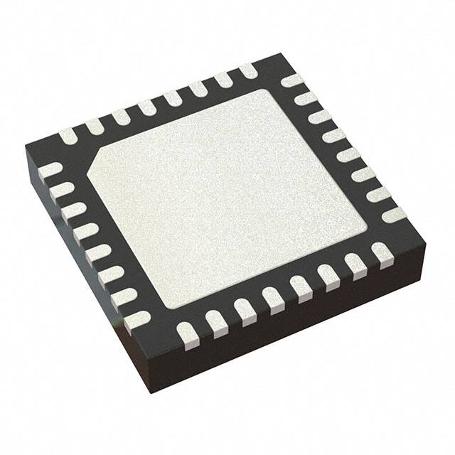
ZL30108
SONET/SDH
Network Interface DPLL
Data Sheet
May 2009
Features
•
Ordering Information
Supports output wander and jitter generation
specifications for GR-253-CORE OC-3 and G.813
STM-1 SONET/SDH interfaces
•
Accepts two input references and synchronizes to
any combination of 2 kHz, 8 kHz, 1.544 MHz,
2.048 MHz, 8.192 MHz, 16.384 MHz or 19.44 MHz
inputs
•
Provides a 19.44 MHz (SONET/SDH) clock output
•
Provides an 8 kHz framing pulse and a 2 kHz
multi-frame pulse
•
Provides automatic entry into Holdover and return
from Holdover
•
Hitless reference switching between any
combination of valid input reference frequencies
•
Provides lock and accurate reference fail
indication
•
Loop filter bandwidth of 29 Hz or 14 Hz
•
Less than 24 psrms intrinsic jitter on the 19.44 MHz
output clock, compliant with GR-253-CORE OC-3
and G.813 STM-1 specifications
•
Less than 0.5 nspp intrinsic jitter on output frame
pulses
•
External master clock source: clock oscillator or
crystal
•
Simple hardware control interface
OSCi
OSCo
ZL30108LDA
ZL30108LDG1
32 Pin QFN
Tubes, Bake & Drypack
32 Pin QFN* Trays, Bake & Drypack
*Pb Free Matte Tin
-40°C to +85°C
Applications
•
Line card synchronization for SONET/SDH
systems
Description
The ZL30108 SONET/SDH network interface digital
phase-locked loop (DPLL) provides timing and
synchronization for SONET/SDH network interface
cards.
The ZL30108 generates a SONET/SDH clock and
framing signals that are phase locked to one of two
backplane or network references. It helps ensure
system reliability by monitoring its references for
frequency accuracy and stability and by maintaining
tight phase alignment between the input reference
clock and clock outputs.
The ZL30108 output clock’s wander and jitter
generation are compliant with GR-253-CORE OC-3
and G.813 STM-1 specifications.
LOCK
TIE_CLR
Master Clock
REF0
TIE
Corrector
Circuit
MUX
REF1
REF_FAIL0
REF_FAIL1
OOR_SEL
Reference
Monitor
DPLL
Frequency
Synthesizer
TIE
Corrector
Enable
Mode
Control
REF_SEL
RST
Virtual
Reference
State Machine
Frequency
Select
MODE_SEL
Figure 1 - Functional Block Diagram
1
Zarlink Semiconductor Inc.
Zarlink, ZL and the Zarlink Semiconductor logo are trademarks of Zarlink Semiconductor Inc.
Copyright 2004-2009, Zarlink Semiconductor Inc. All Rights Reserved.
C19o
F8ko
F2ko
�ZL30108
1.0
Data Sheet
Change Summary
Changes from March 2006 Issue. Page, section, figure and table numbers refer to this current issue.
Page
Item
Change
1
Ordering Information
Updates to Packaging Information. Added new packaging
variants. Added Section 9.0.
Changes from November 2005 Issue. Page, section, figure and table numbers refer to this current issue.
Page
Item
Change
1
Ordering Information
Updated Ordering Information.
Changes from July 2005 Issue. Page, section, figure and table numbers refer to this current issue.
Page
Item
Change
1
Features
Changed description for hitless reference switching.
18
Section 7.1
Removed power supply decoupling circuit and included
reference to synchronizer power supply decoupling application
note.
Changes from October 2004 Issue to July 2005 Issue. Page, section, figure and table numbers refer to this issue.
Page
Item
Change
6
RST pin
Specified clock and frame pulse outputs forced to high
impedance.
20
Section 7.4
Corrected time-constant of example reset circuit.
21
Table “DC Electrical Characteristics*“
Corrected Schmitt trigger levels.
25
Table “Performance Characteristics* Functional“
Specified TIE_CLR=1 in Lock Time conditions.
2
Zarlink Semiconductor Inc.
�ZL30108
Data Sheet
Table of Contents
1.0 Change Summary . . . . . . . . . . . . . . . . . . . . . . . . . . . . . . . . . . . . . . . . . . . . . . . . . . . . . . . . . . . . . . . . . . . . . . 2
2.0 Physical Description . . . . . . . . . . . . . . . . . . . . . . . . . . . . . . . . . . . . . . . . . . . . . . . . . . . . . . . . . . . . . . . . . . . . 5
2.1 Pin Connections . . . . . . . . . . . . . . . . . . . . . . . . . . . . . . . . . . . . . . . . . . . . . . . . . . . . . . . . . . . . . . . . . . . . . 5
3.0 Pin Description. . . . . . . . . . . . . . . . . . . . . . . . . . . . . . . . . . . . . . . . . . . . . . . . . . . . . . . . . . . . . . . . . . . . . . . . . 6
4.0 Functional Description . . . . . . . . . . . . . . . . . . . . . . . . . . . . . . . . . . . . . . . . . . . . . . . . . . . . . . . . . . . . . . . . . . 8
4.1 Reference Select Multiplexer (MUX) . . . . . . . . . . . . . . . . . . . . . . . . . . . . . . . . . . . . . . . . . . . . . . . . . . . . . . 8
4.2 Reference Monitor . . . . . . . . . . . . . . . . . . . . . . . . . . . . . . . . . . . . . . . . . . . . . . . . . . . . . . . . . . . . . . . . . . . . 8
4.3 Time Interval Error (TIE) Corrector Circuit. . . . . . . . . . . . . . . . . . . . . . . . . . . . . . . . . . . . . . . . . . . . . . . . . 10
4.4 Digital Phase Lock Loop (DPLL) . . . . . . . . . . . . . . . . . . . . . . . . . . . . . . . . . . . . . . . . . . . . . . . . . . . . . . . . 12
4.5 Frequency Synthesizers . . . . . . . . . . . . . . . . . . . . . . . . . . . . . . . . . . . . . . . . . . . . . . . . . . . . . . . . . . . . . . 13
4.6 State Machine . . . . . . . . . . . . . . . . . . . . . . . . . . . . . . . . . . . . . . . . . . . . . . . . . . . . . . . . . . . . . . . . . . . . . . 13
4.7 Master Clock . . . . . . . . . . . . . . . . . . . . . . . . . . . . . . . . . . . . . . . . . . . . . . . . . . . . . . . . . . . . . . . . . . . . . . . 13
5.0 Control and Modes of Operation . . . . . . . . . . . . . . . . . . . . . . . . . . . . . . . . . . . . . . . . . . . . . . . . . . . . . . . . . 14
5.1 Out of Range Selection . . . . . . . . . . . . . . . . . . . . . . . . . . . . . . . . . . . . . . . . . . . . . . . . . . . . . . . . . . . . . . . 14
5.2 Modes of Operation . . . . . . . . . . . . . . . . . . . . . . . . . . . . . . . . . . . . . . . . . . . . . . . . . . . . . . . . . . . . . . . . . . 14
5.2.1 Freerun Mode. . . . . . . . . . . . . . . . . . . . . . . . . . . . . . . . . . . . . . . . . . . . . . . . . . . . . . . . . . . . . . . . . . 14
5.2.2 Normal Mode . . . . . . . . . . . . . . . . . . . . . . . . . . . . . . . . . . . . . . . . . . . . . . . . . . . . . . . . . . . . . . . . . . 14
5.3 Reference Selection . . . . . . . . . . . . . . . . . . . . . . . . . . . . . . . . . . . . . . . . . . . . . . . . . . . . . . . . . . . . . . . . . 16
6.0 Measures of Performance . . . . . . . . . . . . . . . . . . . . . . . . . . . . . . . . . . . . . . . . . . . . . . . . . . . . . . . . . . . . . . . 16
6.1 Jitter Generation (Intrinsic Jitter) . . . . . . . . . . . . . . . . . . . . . . . . . . . . . . . . . . . . . . . . . . . . . . . . . . . . . . . . 16
6.2 Jitter Tolerance . . . . . . . . . . . . . . . . . . . . . . . . . . . . . . . . . . . . . . . . . . . . . . . . . . . . . . . . . . . . . . . . . . . . . 16
6.3 Jitter Transfer . . . . . . . . . . . . . . . . . . . . . . . . . . . . . . . . . . . . . . . . . . . . . . . . . . . . . . . . . . . . . . . . . . . . . . 16
6.4 Frequency Accuracy . . . . . . . . . . . . . . . . . . . . . . . . . . . . . . . . . . . . . . . . . . . . . . . . . . . . . . . . . . . . . . . . . 16
6.5 Holdover Accuracy . . . . . . . . . . . . . . . . . . . . . . . . . . . . . . . . . . . . . . . . . . . . . . . . . . . . . . . . . . . . . . . . . . 17
6.6 Capture Range . . . . . . . . . . . . . . . . . . . . . . . . . . . . . . . . . . . . . . . . . . . . . . . . . . . . . . . . . . . . . . . . . . . . . 17
6.7 Lock Range . . . . . . . . . . . . . . . . . . . . . . . . . . . . . . . . . . . . . . . . . . . . . . . . . . . . . . . . . . . . . . . . . . . . . . . . 17
6.8 Time Interval Error (TIE) . . . . . . . . . . . . . . . . . . . . . . . . . . . . . . . . . . . . . . . . . . . . . . . . . . . . . . . . . . . . . . 17
6.9 Maximum Time Interval Error (MTIE) . . . . . . . . . . . . . . . . . . . . . . . . . . . . . . . . . . . . . . . . . . . . . . . . . . . . 17
6.10 Phase Continuity . . . . . . . . . . . . . . . . . . . . . . . . . . . . . . . . . . . . . . . . . . . . . . . . . . . . . . . . . . . . . . . . . . . 17
6.11 Phase Lock Time. . . . . . . . . . . . . . . . . . . . . . . . . . . . . . . . . . . . . . . . . . . . . . . . . . . . . . . . . . . . . . . . . . . 17
7.0 Applications . . . . . . . . . . . . . . . . . . . . . . . . . . . . . . . . . . . . . . . . . . . . . . . . . . . . . . . . . . . . . . . . . . . . . . . . . . 18
7.1 Power Supply Decoupling . . . . . . . . . . . . . . . . . . . . . . . . . . . . . . . . . . . . . . . . . . . . . . . . . . . . . . . . . . . . . 18
7.2 Master Clock . . . . . . . . . . . . . . . . . . . . . . . . . . . . . . . . . . . . . . . . . . . . . . . . . . . . . . . . . . . . . . . . . . . . . . . 18
7.2.1 Clock Oscillator . . . . . . . . . . . . . . . . . . . . . . . . . . . . . . . . . . . . . . . . . . . . . . . . . . . . . . . . . . . . . . . . 18
7.2.2 Crystal Oscillator . . . . . . . . . . . . . . . . . . . . . . . . . . . . . . . . . . . . . . . . . . . . . . . . . . . . . . . . . . . . . . . 19
7.3 Power Up Sequence . . . . . . . . . . . . . . . . . . . . . . . . . . . . . . . . . . . . . . . . . . . . . . . . . . . . . . . . . . . . . . . . . 20
7.4 Reset Circuit . . . . . . . . . . . . . . . . . . . . . . . . . . . . . . . . . . . . . . . . . . . . . . . . . . . . . . . . . . . . . . . . . . . . . . . 20
8.0 Characteristics . . . . . . . . . . . . . . . . . . . . . . . . . . . . . . . . . . . . . . . . . . . . . . . . . . . . . . . . . . . . . . . . . . . . . . . . 21
8.1 AC and DC Electrical Characteristics . . . . . . . . . . . . . . . . . . . . . . . . . . . . . . . . . . . . . . . . . . . . . . . . . . . . 21
8.2 Performance Characteristics . . . . . . . . . . . . . . . . . . . . . . . . . . . . . . . . . . . . . . . . . . . . . . . . . . . . . . . . . . . 25
9.0 Packaging Information . . . . . . . . . . . . . . . . . . . . . . . . . . . . . . . . . . . . . . . . . . . . . . . . . . . . . . . . . . . . . . . . . 27
3
Zarlink Semiconductor Inc.
�ZL30108
Data Sheet
List of Figures
Figure 1 - Functional Block Diagram . . . . . . . . . . . . . . . . . . . . . . . . . . . . . . . . . . . . . . . . . . . . . . . . . . . . . . . . . . . . 1
Figure 2 - Pin Connections (32 pin 5 mm X 5 mm QFN) . . . . . . . . . . . . . . . . . . . . . . . . . . . . . . . . . . . . . . . . . . . . . 5
Figure 3 - Reference Monitor Circuit . . . . . . . . . . . . . . . . . . . . . . . . . . . . . . . . . . . . . . . . . . . . . . . . . . . . . . . . . . . . 8
Figure 4 - Behavior of the Dis/Requalify Timer . . . . . . . . . . . . . . . . . . . . . . . . . . . . . . . . . . . . . . . . . . . . . . . . . . . . 9
Figure 5 - Out-of-Range Thresholds for OOR_SEL=1. . . . . . . . . . . . . . . . . . . . . . . . . . . . . . . . . . . . . . . . . . . . . . . 9
Figure 6 - Out-of-Range Thresholds for OOR_SEL=0. . . . . . . . . . . . . . . . . . . . . . . . . . . . . . . . . . . . . . . . . . . . . . 10
Figure 7 - Timing Diagram of Hitless Reference Switching . . . . . . . . . . . . . . . . . . . . . . . . . . . . . . . . . . . . . . . . . . 11
Figure 8 - DPLL Block Diagram . . . . . . . . . . . . . . . . . . . . . . . . . . . . . . . . . . . . . . . . . . . . . . . . . . . . . . . . . . . . . . . 12
Figure 9 - Mode Switching in Normal Mode . . . . . . . . . . . . . . . . . . . . . . . . . . . . . . . . . . . . . . . . . . . . . . . . . . . . . . 15
Figure 10 - Clock Oscillator Circuit. . . . . . . . . . . . . . . . . . . . . . . . . . . . . . . . . . . . . . . . . . . . . . . . . . . . . . . . . . . . . 18
Figure 11 - Crystal Oscillator Circuit. . . . . . . . . . . . . . . . . . . . . . . . . . . . . . . . . . . . . . . . . . . . . . . . . . . . . . . . . . . . 19
Figure 12 - Power-Up Reset Circuit . . . . . . . . . . . . . . . . . . . . . . . . . . . . . . . . . . . . . . . . . . . . . . . . . . . . . . . . . . . . 20
Figure 13 - Timing Parameter Measurement Voltage Levels. . . . . . . . . . . . . . . . . . . . . . . . . . . . . . . . . . . . . . . . . 22
Figure 14 - Input to Output Timing . . . . . . . . . . . . . . . . . . . . . . . . . . . . . . . . . . . . . . . . . . . . . . . . . . . . . . . . . . . . . 24
Figure 15 - SONET/SDH Output Timing Referenced to F8ko . . . . . . . . . . . . . . . . . . . . . . . . . . . . . . . . . . . . . . . . 24
4
Zarlink Semiconductor Inc.
�24
22
AGND
REF_SEL
20
AGND
Data Sheet
AVCORE
AVDD
F2ko
Pin Connections
C19o
2.1
AGND
Physical Description
F8ko
2.0
AVDD
ZL30108
18
16
ZL30108
26
AVDD
REF0
REF1
14
12
30
OSCi
OSCo
33
VDD
IC (E-pad)
10
32
GND
8
AVCORE
VCORE
6
REF_FAIL1
4
LOCK
VCORE
GND
RST
MODE_SEL
2
REF_FAIL0
TIE_CLR
VDD
IC
28
OOR_SEL
IC
GND
Figure 2 - Pin Connections (32 pin 5 mm X 5 mm QFN)
5
Zarlink Semiconductor Inc.
�ZL30108
3.0
Data Sheet
Pin Description
Pin #
Name
Description
1
GND
2
VCORE
Positive Supply Voltage. +1.8 VDC nominal
3
LOCK
Lock Indicator (Output). This output goes to a logic high when the PLL is frequency
locked to the selected input reference.
4
REF_FAIL0
Reference 0 Failure Indicator (Output). A logic high at this pin indicates that the REF0
reference frequency has exceeded the out-of-range limit set by the OOR_SEL pin or that
it is exhibiting abrupt phase or frequency changes.
5
REF_FAIL1
Reference 1 Failure Indicator (Output). A logic high at this pin indicates that the REF1
reference frequency has exceeded the out-of-range limit set by the OOR_SEL pin or that
it is exhibiting abrupt phase or frequency changes.
6
VCORE
7
AVCORE
8
GND
9
MODE_SEL
10
RST
Reset (Input). A logic low at this input resets the device. On power up, the RST pin must
be held low for a minimum of 300 ns after the power supply pins have reached the
minimum supply voltage. When the RST pin goes high, the device will transition into a
Reset state for 3 ms. In the Reset state all clock and frame pulse outputs will be forced
into high impedance.
11
OSCo
Oscillator Master Clock (Output). For crystal operation, a 20 MHz crystal is connected
from this pin to OSCi. This output is not suitable for driving other devices. For clock
oscillator operation, this pin must be left unconnected.
12
OSCi
Oscillator Master Clock (Input). For crystal operation, a 20 MHz crystal is connected
from this pin to OSCo. For clock oscillator operation, this pin must be connected to a
clock source.
13
IC
14
VDD
Positive Supply Voltage. +3.3 VDC nominal
15
AVDD
Positive Analog Supply Voltage. +3.3 VDC nominal
16
GND
Ground. 0 V
17
AGND
18
AVCORE
Positive Analog Supply Voltage. +1.8 VDC nominal
19
AVDD
Positive Analog Supply Voltage. +3.3 VDC nominal
20
F2ko
Multi Frame Pulse (Output). This is a CMOS 2 kHz active high 51 ns framing pulse,
which marks the beginning of a multi frame.
Ground. 0 V
Positive Supply Voltage. +1.8 VDC nominal.
Positive Analog Supply Voltage. +1.8 VDC nominal.
Ground. 0 V
Mode Select (Input). This input determines the mode of operation: See Table 3.
0: Normal mode (device locked to input reference)
1: Freerun mode
Internal Connection. Connect this pin to VDD.
Analog Ground. 0 V
This clock output pad includes a Schmitt triggered input which serves as a PLL feedback
path; proper transmission-line termination should be applied to maintain reflections below
Schmitt trigger levels.
6
Zarlink Semiconductor Inc.
�ZL30108
Pin #
Name
21
C19o
Data Sheet
Description
Clock 19.44 MHz (Output). This CMOS output is used in SONET/SDH applications.
This clock output pad includes a Schmitt input which serves as a PLL feedback path;
proper transmission-line termination should be applied to maintain reflections below
Schmitt trigger levels.
22
AGND
Analog Ground. 0 V
23
AVDD
Positive Analog Supply Voltage. +3.3 VDC nominal
24
F8ko
Frame Pulse (Output). This is an CMOS 8 kHz active high 31 ns framing pulse, which
marks the beginning of a 125 μs frame.
This clock output pad includes a Schmitt input which serves as a PLL feedback path;
proper transmission-line termination should be applied to maintain reflections below
Schmitt trigger levels.
25
AGND
Analog Ground. 0 V
26
REF_SEL
27
REF0
Reference (Input). This is one of two (REF0 and REF1) input reference sources used for
synchronization. One of seven possible frequencies may be used: 2 kHz, 8 kHz,
1.544 MHz, 2.048 MHz, 8.192 MHz,16.384 MHz or 19.44 MHz. This pin is internally
pulled down to GND.
28
REF1
Reference (Input). See REF0 pin description.
29
OOR_SEL
30
IC
31
VDD
32
TIE_CLR
33
IC
Reference Select 0 (Input/Output). As an input REF_SEL selects the reference input
that is used for synchronization; See Table 4.
0: REF0
1: REF1
This pin is internally pulled down to GND.
Out Of Range Selection (Input). This input selects the frequency acceptance limits of
the reference monitor: See Table 2.
0: 40 - 52 ppm
1: 64 - 83 ppm
Internal Connection. Connect this pin to GND.
Positive Supply Voltage. +3.3 VDC nominal.
TIE Circuit Reset (Input). A logic low at this input resets the Time Interval Error (TIE)
correction circuit resulting in a realignment of input phase with output phase.
Internal Connection. Package E-pad, this pin is internally connected to device GND, it
can be left unconnected or it can be connected to GND.
7
Zarlink Semiconductor Inc.
�ZL30108
4.0
Data Sheet
Functional Description
The ZL30108 is a SONET/SDH Network Interface DPLL, providing timing (clock) and synchronization (frame)
signals to SONET/SDH network interface cards. Figure 1 is a functional block diagram which is described in the
following sections.
4.1
Reference Select Multiplexer (MUX)
The ZL30108 accepts two simultaneous reference input signals and operates on their rising edges. One of two, the
primary reference (REF0) or the secondary reference (REF1) signal is selected as input to the TIE Corrector Circuit
based on the Reference Selection (REF_SEL) input.
4.2
Reference Monitor
The input references are monitored by two independent reference monitor blocks, one for each reference. The
block diagram of a single reference monitor is shown in Figure 3. For each reference clock, the frequency is
detected and the clock is continuously monitored for three independent criteria that indicate abnormal behavior of
the reference signal, for example; long term drift from its nominal frequency or excessive jitter. To ensure proper
operation of the reference monitor circuit, the minimum input pulse width restriction of 15 nsec must be
observed.
•
Reference Frequency Detector (RFD): This detector determines whether the frequency of the reference
clock is 2 kHz, 8 kHz, 1.544 MHz, 2.048 MHz 8.192 MHz, 16.384 MHz or 19.44 MHz and provides this
information to the various monitor circuits and the phase detector circuit of the DPLL.
•
Precise Frequency Monitor (PFM): This circuit determines whether the frequency of the reference clock
is within the applicable accuracy range defined by the OOR_SEL pin, see Figure 5, Figure 6 and Table 2.
It will take the precise frequency monitor up to 10 s to qualify or disqualify the input reference.
•
Coarse Frequency Monitor (CFM): This circuit monitors the reference over intervals of approximately
30 µs to quickly detect large frequency changes.
•
Single Cycle Monitor (SCM): This detector checks the period of a single clock cycle to detect large
phase hits or the complete loss of the clock.
Reference Frequency
Detector
REF0 /
REF1
REF_FAIL0 /
REF_FAIL1
OR
Precise Frequency
Monitor
Coarse Frequency
Monitor
Single Cycle
Monitor
dis/requalify
timer
REF_DIS Mode select
state machine
OR
HOLDOVER
REF_DIS= reference disrupted (internal signal)
Figure 3 - Reference Monitor Circuit
8
Zarlink Semiconductor Inc.
�ZL30108
Data Sheet
Exceeding the threshold of any of the monitors forces the corresponding REF_FAIL pin to go high. The single cycle
and coarse frequency failure flags force the DPLL into Holdover mode and feed a timer that disqualifies the
reference input signal when the failures are present for more than 2.5 s. The single cycle and coarse frequency
failures must be absent for 10 s to let the timer requalify the input reference signal as valid. Multiple failures of less
than 2.5 s each have an accumulative effect and will disqualify the reference. This is illustrated in Figure 4.
SCM or CFM failure
current REF
timer
2.5 s
10 s
REF_FAIL
HOLDOVER
Figure 4 - Behavior of the Dis/Requalify Timer
When the incoming signal returns to normal (REF_FAIL=0), the DPLL returns to Normal mode with the output
signal locked to the input signal. Each of the monitors has a built-in hysteresis to prevent flickering of the REF_FAIL
status pin at the threshold boundaries. The precise frequency monitor and the timer do not affect the mode
(Holdover/Normal) of the DPLL.
C20i Clock Accuracy
Out of Range
C20
0 ppm
In Range
-83
-64
0
64
83
Out of Range
C20
+32 ppm
In Range
-51
96
32
-32
115
Out of Range
C20
-32 ppm
In Range
-115
-96
-100
-32
-75
-50
-25
32
0
25
51
50
75
100
Figure 5 - Out-of-Range Thresholds for OOR_SEL=1
9
Zarlink Semiconductor Inc.
Frequency offset [ppm]
�ZL30108
Data Sheet
C20i Clock Accuracy
Out of Range
C20
0 ppm
In Range
-52 -40
0
40 52
Out of Range
C20
+20 ppm
In Range
-32
-20
60
20
72
Out of Range
C20
-20 ppm
In Range
-72 -60
-100
-75
-50
20
-32
-25
0
32
25
50
75
100
Frequency offset [ppm]
Figure 6 - Out-of-Range Thresholds for OOR_SEL=0
4.3
Time Interval Error (TIE) Corrector Circuit
The TIE Corrector Circuit eliminates phase transients on the output clock that may occur in the course of recovery
from Automatic Holdover mode to Normal mode.
On recovery from Automatic Holdover mode or when switching to another reference input, the TIE corrector circuit
measures the phase delay between the current phase (feedback signal) and the phase of the selected reference
signal. This delay value is stored in the TIE corrector circuit. This circuit creates a new virtual reference signal that
is at the same phase position as the feedback signal. By using the virtual reference, the PLL minimizes the phase
transient it experiences when it switches to another reference input or recovers from Automatic Holdover mode.
The delay value can be reset by setting the TIE Corrector Circuit Clear pin (TIE_CLR) low for at least 15 ns. This
results in a phase alignment between the input reference signal and the output clocks and frame pulses as shown
in Figure 14 and Figure 15. The speed of the phase alignment correction is limited by the loop filter bandwidth.
Convergence is always in the direction of least phase travel. TIE_CLR can be kept low continuously. In that case
the output clocks will always align with the selected input reference. This is illustrated in Figure 7.
10
Zarlink Semiconductor Inc.
�ZL30108
Data Sheet
TIE_CLR = 0
TIE_CLR = 1
locked to REF0
locked to REF0
REF0
REF0
REF1
REF1
Output
Clock
Output
Clock
locked to REF1
locked to REF1
REF0
REF0
REF1
REF1
Output
Clock
Output
Clock
Figure 7 - Timing Diagram of Hitless Reference Switching
11
Zarlink Semiconductor Inc.
�ZL30108
4.4
Data Sheet
Digital Phase Lock Loop (DPLL)
The DPLL of the ZL30108 consists of a phase detector, an integrated on-chip loop filter, and a digitally controlled
oscillator as shown in Figure 8. The data path from the phase detector to the filter is tapped and routed to the lock
indicator that provides a lock indication which is output at the LOCK pin.
lock
indicator
virtual reference
from
TIE corrector circuit
phase
detector
loop filter
digitally
controlled
oscillator
LOCK
DPLL reference to
frequency synthesizer
state select from
control state machine
feedback signal from
frequency select MUX
Figure 8 - DPLL Block Diagram
Phase Detector - the phase detector compares the virtual reference signal from the TIE corrector circuit with the
feedback signal and provides an error signal corresponding to the phase difference between the two. This error
signal is passed to the loop filter circuit.
Loop Filter - the loop filter is similar to a first order low pass filter with bandwidth of 29 Hz, suitable to provide timing
and synchronization for SONET/SDH network interface cards.
Detected REF Frequency
Loop Filter Bandwidth
2 kHz
14 Hz
8 kHz, 1.544 MHz,
2.048 MHz, 8.192 MHz,
16.384 MHz, 19.44 MHz
29 Hz
Table 1 - Loop Filter Bandwidth Settings
12
Zarlink Semiconductor Inc.
�ZL30108
Data Sheet
Digitally Controlled Oscillator (DCO) - the DCO receives the limited and filtered signal from the Loop Filter, and
based on its value, generates a corresponding digital output signal. The synchronization method of the DCO is
dependent on the state of the ZL30108.
In Normal Mode, the DCO provides an output signal which is frequency and phase locked to the selected input
reference signal.
In the Automatic Holdover mode, the DCO is free running at a frequency equal to the frequency that the DCO was
generating in Normal Mode. The frequency in the Automatic Holdover mode is calculated from frequency samples
stored 26 ms to 52 ms before the ZL30108 entered the Automatic Holdover mode. This ensures that the coarse
frequency monitor and the single cycle monitor have time to disqualify a bad reference before it corrupts the
holdover frequency.
In Freerun Mode, the DCO is free running with an accuracy equal to the accuracy of the OSCi 20 MHz source.
Lock Indicator - the lock detector monitors if the output value of the phase detector is within the phase-lockwindow for a certain time. The selected phase-lock-window guarantees the stable operation of the LOCK pin with
maximum network jitter and wander on the reference input. If the DPLL goes into the Automatic Holdover mode, the
LOCK pin will initially stay high for 0.1 s. If at that point the DPLL is still in the Automatic Holdover mode, the LOCK
pin will go low. In Freerun mode the LOCK pin will go low immediately.
4.5
Frequency Synthesizers
The output of the DCO is used by the frequency synthesizers to generate the output clocks and frame pulses which
are synchronized to one of the input references (REF0 or REF1).
The frequency synthesizer uses digital techniques to generate output clocks and advanced noise shaping
techniques to minimize the output jitter. The clock and frame pulse outputs have limited drive capability and should
be buffered when driving high capacitance loads.
4.6
State Machine
As shown in Figure 1, the state machine controls the TIE Corrector Circuit and the DPLL. The control of the
ZL30108 is based on the input MODE_SEL.
4.7
Master Clock
The ZL30108 can use either a clock or crystal as the master timing source. For recommended master timing
circuits, see the Applications - Master Clock section.
13
Zarlink Semiconductor Inc.
�ZL30108
5.0
Control and Modes of Operation
5.1
Out of Range Selection
Data Sheet
The frequency out of range limits for the precise frequency monitoring in the reference monitors are selected by the
OOR_SEL pin, see Table 2.
OOR_SEL
Out Of Range Limits
0
40 - 52 ppm
1
64 - 83 ppm
Table 2 - Out of Range Limits Selection
5.2
Modes of Operation
The ZL30108 has two possible manual modes of operation; Normal and Freerun. These modes are selected with
mode select pins MODE_SEL as is shown in Table 3. Transitioning from one mode to the other is controlled
externally.
MODE_SEL
Mode
0
Normal (with automatic Holdover)
1
Freerun
Table 3 - Operating Modes
5.2.1
Freerun Mode
Freerun mode is typically used when an independent clock source is required, or immediately following system
power-up before network synchronization is achieved.
In Freerun mode, the ZL30108 provides timing and synchronization signals which are based on the master clock
frequency (supplied to OSCi pin) only, and are not synchronized to the reference input signals.
The accuracy of the output clock is equal to the accuracy of the master clock (OSCi). So if a ±32 ppm output clock
is required, the master clock must also be ±32 ppm. See Applications - Section 7.2, “Master Clock“.
5.2.2
Normal Mode
Normal mode is typically used when a system clock source, synchronized to the network or a backplane is required.
In Normal mode, the ZL30108 provides timing and frame synchronization signals, which are synchronized to one of
two reference inputs (REF0 or REF1). The input reference signal may have a nominal frequency of 2 kHz, 8 kHz,
1.544 MHz, 2.048 MHz, 8.192 MHz, 16.384 MHz or 19.44 MHz. The frequency of the reference inputs are
automatically detected by the reference monitors.
When the Normal mode is selected through the MODE_SEL pin, the ZL30108 will automatically go into the
Automatic Holdover mode if the currently selected reference is disrupted (see Figure 9). After the power up reset,
the ZL30108 will initially go into the Automatic Holdover mode, generating clocks with the same accuracy as it
would be in the Freerun mode. If the currently selected reference is not disrupted (see Figure 3), the state machine
takes the DPLL out of the Automatic Holdover mode. The transition is done through the TIE correction state and the
current phase offset of the output signals to the input reference is maintained.
14
Zarlink Semiconductor Inc.
�ZL30108
Data Sheet
If the current reference experiences an disruption while the device is in Normal mode, the device will go
automatically into Automatic Holdover mode. It will return to Normal mode as soon as the reference is valid again.
If the reference selection changes because the value of the REF_SEL pin change the ZL30108 goes into Automatic
Holdover mode and returns to Normal mode through the TIE correction state.
Normal
(locked)
REF_DIS=0 and
REF_CH=0
REF_CH=1
REF_DIS=0
RST
REF_DIS=1
REF_DIS=1
TIE Correction
Holdover
(REF_DIS=0) or
REF_CH=1
REF_DIS=1: Current selected reference disrupted (see Figure 3)
REF_CH= 1: Reference change, a transition in the reference selection (a change in the
REF_SEL pin).
Figure 9 - Mode Switching in Normal Mode
Automatic Holdover Mode
Automatic Holdover mode is typically used for short durations while system synchronization is temporarily
disrupted.
In Automatic Holdover mode, the ZL30108 provides timing and synchronization signals, which are not locked to an
external reference signal, but are based on storage techniques. The storage value is determined while the device is
in Normal Mode and locked to an external reference signal.
When in Normal Mode, and locked to the input reference signal, a numerical value corresponding to the ZL30108
output reference frequency is stored alternately in two memory locations every 26 ms. When the device is switched
into Automatic Holdover mode, the value in memory from between 26 ms and 52 ms is used to set the output
frequency of the device. The frequency accuracy of Automatic Holdover mode is 0.01 ppm.
Two factors affect the accuracy of Automatic Holdover mode. One is drift on the master clock while in Automatic
Holdover mode, drift on the master clock directly affects the Automatic Holdover mode accuracy. Note that the
absolute master clock (OSCi) accuracy does not affect Holdover accuracy, only the change in OSCi accuracy while
in Holdover. For example, a ±32 ppm master clock may have a temperature coefficient of ±0.1 ppm per °C. So a
±10 °C change in temperature, while the ZL30108 is in the Automatic Holdover mode may result in an additional
offset (over the 0.01 ppm) in frequency accuracy of ±1 ppm, which is much greater than the 0.01 ppm of the
ZL30108. The other factor affecting the accuracy is large jitter on the reference input prior (26 ms to 52 ms) to the
mode switch.
15
Zarlink Semiconductor Inc.
�ZL30108
5.3
Data Sheet
Reference Selection
The active reference input (REF0 or REF1) is selected by the REF_SEL pin as shown in Table 4. If the logic value
of the REF_SEL pin is changed when the DPLL is in Normal mode, the ZL30108 will perform a hitless reference
switch.
REF_SEL
(input pin)
Input Reference Selected
0
REF0
1
REF1
Table 4 - Manual Reference Selection
When the REF_SEL inputs are used to force a change from the currently selected reference to another reference,
the action of the LOCK output will depend on the relative frequency and phase offset of the old and new references.
Where the new reference has enough frequency offset and/or TIE-corrected phase offset to force the output
outside the phase-lock-window, the LOCK output will de-assert, the lock-qualify timer is reset, and LOCK will stay
de-asserted for the full lock-time duration. Where the new reference is close enough in frequency and TIEcorrected phase for the output to stay within the phase-lock-window, the LOCK output will remain asserted through
the reference-switch process.
6.0
Measures of Performance
The following are some PLL performance indicators and their corresponding definitions.
6.1
Jitter Generation (Intrinsic Jitter)
Timing jitter is defined as the high frequency variation of the clock edges from their ideal positions in time. Wander
is defined as the low-frequency variation of the clock edges from their ideal positions in time. High and low
frequency variation imply phase oscillation frequencies relative to some demarcation frequency. (Often 10 Hz or
20 Hz for DS1 or E1, higher for SONET/SDH clocks.) Jitter parameters given in this data sheet are total timing jitter
numbers, not cycle-to-cycle jitter.
6.2
Jitter Tolerance
Jitter tolerance is a measure of the ability of a PLL to operate properly (i.e., remain in lock and or regain lock in the
presence of large jitter magnitudes at various jitter frequencies) when jitter is applied to its reference. The applied
jitter magnitude and jitter frequency depends on the applicable standards.
6.3
Jitter Transfer
Jitter transfer or jitter attenuation refers to the magnitude of jitter at the output of a device for a given amount of jitter
at the input of the device. Input jitter is applied at various amplitudes and frequencies, and output jitter is measured
with various filters depending on the applicable standards. For the ZL30108, the internal low pass loop filter
determines the jitter attenuation.
Since intrinsic jitter is always present, jitter attenuation will appear to be lower for small input jitter signals than for
large ones. Consequently, accurate jitter transfer function measurements are usually made with large input jitter
signals (for example 75% of the specified maximum tolerable input jitter).
6.4
Frequency Accuracy
Frequency accuracy is defined as the absolute accuracy of an output clock signal when it is not locked to an
external reference, but is operating in a free running mode. For the ZL30108, the Freerun accuracy is equal to the
master clock (OSCi) accuracy.
16
Zarlink Semiconductor Inc.
�ZL30108
6.5
Data Sheet
Holdover Accuracy
Holdover accuracy is defined as the absolute frequency accuracy of an output clock signal, when it is not locked to
an external reference signal, but is operating using storage techniques. For the ZL30108, the storage value is
determined while the device is in Normal Mode and locked to an external reference signal.
6.6
Capture Range
Also referred to as pull-in range. This is the input frequency range over which the PLL must be able to pull into
synchronization. The ZL30108 capture range is equal to ±130 ppm minus the accuracy of the master clock (OSCi).
For example, a +32 ppm master clock results in a capture range of +162 ppm on one side and -98 ppm on the other
side of frequency range.
6.7
Lock Range
This is the input frequency range over which the synchronizer must be able to maintain synchronization. The lock
range is equal to the capture range for the ZL30108.
6.8
Time Interval Error (TIE)
TIE is the time delay between a given timing signal and an ideal timing signal.
6.9
Maximum Time Interval Error (MTIE)
MTIE is the maximum peak to peak delay between a given timing signal and an ideal timing signal within a
particular observation period.
6.10
Phase Continuity
Phase continuity is the phase difference between a given timing signal and an ideal timing signal at the end of a
particular observation period. Usually, the given timing signal and the ideal timing signal are of the same frequency.
Phase continuity applies to the output of the PLL after a signal disturbance due to a reference switch or a mode
change. The observation period is usually the time from the disturbance, to just after the synchronizer has settled to
a steady state.
6.11
Phase Lock Time
This is the time it takes the PLL to phase lock to the input signal. Phase lock occurs when the input signal and
output signal are aligned in phase with respect to each other within a certain phase distance (not including jitter).
Lock time is affected by many factors which include:
•
initial input to output phase difference
•
initial input to output frequency difference
•
PLL loop filter bandwidth
•
in-lock phase distance
The presence of input jitter makes it difficult to define when the PLL is locked as it may not be able to align its output
to the input within the required phase distance, dependent on the PLL bandwidth and the input jitter amplitude and
frequency.
Although a short lock time is desirable, it is not always possible to achieve due to other synchronizer requirements.
For instance, better jitter transfer performance is achieved with a lower frequency loop filter which increases lock
time. See Section 8.2, “Performance Characteristics“ for Maximum Phase Lock Time.
17
Zarlink Semiconductor Inc.
�ZL30108
7.0
Data Sheet
Applications
This section contains ZL30108 application specific details for power supply decoupling, clock and crystal operation,
reset operation,and control operation.
7.1
Power Supply Decoupling
Jitter levels on the ZL30108 output clocks may increase if the device is exposed to excessive noise on its power
pins. For optimal jitter performance, the ZL30108 device should be isolated from noise on power planes connected
to its 3.3 V and 1.8 V supply pins. For recommended common layout practices, refer to Zarlink Application Note
ZLAN-178.
7.2
Master Clock
The ZL30108 can use either a clock or crystal as the master timing source. Zarlink Application Note ZLAN-68 lists a
number of applicable oscillators and crystals that can be used with the ZL30108.
7.2.1
Clock Oscillator
When selecting a Clock Oscillator, numerous parameters must be considered. These includes absolute frequency,
frequency change over temperature, output rise and fall times, output levels, duty cycle and phase noise.
1
Frequency
20 MHz
2
Tolerance
As required
3
Rise & Fall Time