ZL30410
Multi-service Line Card PLL
Data Sheet
Features
•
•
•
•
•
•
•
•
•
November 2006
Generates clocks for OC-3, STM-1, DS3, E3,
DS2, DS1, E1, 19.44 MHz and ST-BUS
Meets jitter generation requirements for STM-1,
OC-3, DS3, E3, J2 (DS2), E1 and DS1 interfaces
Compatible with GR-253-CORE SONET stratum
3 and G.813 SEC timing compliant clocks
Provides “hit-less” reference switching
Detects frequency of both reference clocks and
synchronizes to any combination of 8 kHz,
1.544 MHz, 2.048 MHz and 19.44 MHz reference
frequencies
Continuously monitors both references for
frequency accuracy exceeding ±12 ppm
Holdover accuracy of 70x10 -12 meets GR-1244
Stratum 3E and ITU-T G.812 requirements
Meets requirements of G.813 Option 1 for SDH
Equipment Clocks (SEC) and GR-1244 for
Stratum 4E and Stratum 4 Clocks
3.3 V power supply
Ordering Information
ZL30410QCC
ZL30410QCG1
-40°C to 85°C
•
•
The ZL30410 is a Multi-service Line Card
Phase-Locked Loop designed to generate multiple
clocks for SONET, SDH and PDH equipment including
timing for ST-BUS and GCI interfaces.
The ZL30410 operates in NORMAL (LOCKED),
HOLDOVER and FREE-RUN modes to ensure that in
the presence of jitter and interruptions to the reference
signals, the generated clocks meet international
standards. The filtering characteristics of the PLL are
hardware pin selectable and they do not require any
external adjustable components. The ZL30410 uses an
external 20 MHz Master Clock Oscillator to provide a
stable timing source for the HOLDOVER operation.
Line Card synchronization for SDH, SONET, DS3,
E3, J2 (DS2), E1 and DS1 interfaces
Timing card synchronization for SDH and PDH
Network Elements
VDD GND
PRI
PRIOR
Primary
Acquisition
PLL
C20i
FCS
Master Clock
Frequency
Calibration
SEC
OE
APLL
Core PLL
MUX
SECOR
Clock generation for ST-BUS and GCI timing
Description
Applications
•
80 Pin LQFP Trays
80 Pin LQFP* Trays, Bake & Drypack
*Pb Free Matte Tin
Clock
Synthesizer
Secondary
Acquisition
PLL
C155P/N
C34/C44
C19o
C16o
C8o
C6o
C4o
C2o
C1.5o
F16o
F8o
F0o
E3DS3/OC3
E3/DS3
RefSel
RESET
JTAG
IEEE
1149.1a
Control State Machine
MS1 MS2
RefAlign
LOCK
HOLDOVER
Figure 1 - Functional Block Diagram
Zarlink Semiconductor US Patent No. 5,602,884, UK Patent No. 0772912,
France Brevete S.G.D.G. 0772912; Germany DBP No. 69502724.7-08
1
Zarlink Semiconductor Inc.
Zarlink, ZL and the Zarlink Semiconductor logo are trademarks of Zarlink Semiconductor Inc.
Copyright 2003-2006, Zarlink Semiconductor Inc. All Rights Reserved.
Tclk
Tdi
Tdo
Tms
Trst
07
�ZL30410
Data Sheet
Table of Contents
1.0 Change Summary . . . . . . . . . . . . . . . . . . . . . . . . . . . . . . . . . . . . . . . . . . . . . . . . . . . . . . . . . . . . . . . . . . . . . . 5
2.0 ZL30410 Pinout . . . . . . . . . . . . . . . . . . . . . . . . . . . . . . . . . . . . . . . . . . . . . . . . . . . . . . . . . . . . . . . . . . . . . . . . 5
2.1 Pin Connections . . . . . . . . . . . . . . . . . . . . . . . . . . . . . . . . . . . . . . . . . . . . . . . . . . . . . . . . . . . . . . . . . . . . . 5
3.0 Functional Description . . . . . . . . . . . . . . . . . . . . . . . . . . . . . . . . . . . . . . . . . . . . . . . . . . . . . . . . . . . . . . . . . 10
3.1 Acquisition PLLs . . . . . . . . . . . . . . . . . . . . . . . . . . . . . . . . . . . . . . . . . . . . . . . . . . . . . . . . . . . . . . . . . . . . 10
3.2 Core PLL . . . . . . . . . . . . . . . . . . . . . . . . . . . . . . . . . . . . . . . . . . . . . . . . . . . . . . . . . . . . . . . . . . . . . . . . . . 10
3.2.1 Digitally Controlled Oscillator (DCO) . . . . . . . . . . . . . . . . . . . . . . . . . . . . . . . . . . . . . . . . . . . . . . . . 11
3.2.2 Filters . . . . . . . . . . . . . . . . . . . . . . . . . . . . . . . . . . . . . . . . . . . . . . . . . . . . . . . . . . . . . . . . . . . . . . . . 11
3.2.3 Lock Indicator (LOCK) . . . . . . . . . . . . . . . . . . . . . . . . . . . . . . . . . . . . . . . . . . . . . . . . . . . . . . . . . . . 11
3.2.4 Reference Alignment (RefAlign). . . . . . . . . . . . . . . . . . . . . . . . . . . . . . . . . . . . . . . . . . . . . . . . . . . . 11
3.2.4.1 Using RefAlign with 1.544 MHz, 2.048 MHz or 19.44 MHz Reference . . . . . . . . . . . . . . . . . 12
3.2.4.2 Using RefAlign with an 8 kHz Reference . . . . . . . . . . . . . . . . . . . . . . . . . . . . . . . . . . . . . . . . 12
3.3 Clock Synthesizer . . . . . . . . . . . . . . . . . . . . . . . . . . . . . . . . . . . . . . . . . . . . . . . . . . . . . . . . . . . . . . . . . . . 12
3.3.1 Output Clocks. . . . . . . . . . . . . . . . . . . . . . . . . . . . . . . . . . . . . . . . . . . . . . . . . . . . . . . . . . . . . . . . . . 12
3.4 Control State Machine . . . . . . . . . . . . . . . . . . . . . . . . . . . . . . . . . . . . . . . . . . . . . . . . . . . . . . . . . . . . . . . . 13
3.4.1 Clock Modes . . . . . . . . . . . . . . . . . . . . . . . . . . . . . . . . . . . . . . . . . . . . . . . . . . . . . . . . . . . . . . . . . . 13
3.4.2 ZL30410 State Machine . . . . . . . . . . . . . . . . . . . . . . . . . . . . . . . . . . . . . . . . . . . . . . . . . . . . . . . . . . 13
3.4.3 State Transitions . . . . . . . . . . . . . . . . . . . . . . . . . . . . . . . . . . . . . . . . . . . . . . . . . . . . . . . . . . . . . . . 15
3.5 JTAG Interface . . . . . . . . . . . . . . . . . . . . . . . . . . . . . . . . . . . . . . . . . . . . . . . . . . . . . . . . . . . . . . . . . . . . . 16
4.0 Control Interface . . . . . . . . . . . . . . . . . . . . . . . . . . . . . . . . . . . . . . . . . . . . . . . . . . . . . . . . . . . . . . . . . . . . . . 16
4.1 Control Pins . . . . . . . . . . . . . . . . . . . . . . . . . . . . . . . . . . . . . . . . . . . . . . . . . . . . . . . . . . . . . . . . . . . . . . . . 16
4.2 Status Pins . . . . . . . . . . . . . . . . . . . . . . . . . . . . . . . . . . . . . . . . . . . . . . . . . . . . . . . . . . . . . . . . . . . . . . . . 17
5.0 Applications . . . . . . . . . . . . . . . . . . . . . . . . . . . . . . . . . . . . . . . . . . . . . . . . . . . . . . . . . . . . . . . . . . . . . . . . . . 18
5.1 ZL30410 Switching Between Clock Modes . . . . . . . . . . . . . . . . . . . . . . . . . . . . . . . . . . . . . . . . . . . . . . . . 18
5.1.1 System Start-up Sequence: FREE-RUN --> HOLDOVER --> NORMAL . . . . . . . . . . . . . . . . . . . . . 18
5.1.2 Single Reference Operation: NORMAL --> AUTO HOLDOVER --> NORMAL . . . . . . . . . . . . . . . . 19
5.1.3 Single 8 kHz Reference Operation: NORMAL --> AUTO HOLDOVER--> HOLDOVER --> NORMAL
20
5.1.4 Dual Reference Operation: NORMAL --> AUTO HOLDOVER--> HOLDOVER --> NORMAL. . . . . 20
5.1.5 Reference Switching (RefSel): NORMAL --> HOLDOVER --> NORMAL . . . . . . . . . . . . . . . . . . . . 21
5.2 Power Supply Filtering. . . . . . . . . . . . . . . . . . . . . . . . . . . . . . . . . . . . . . . . . . . . . . . . . . . . . . . . . . . . . . . . 22
6.0 Characteristics . . . . . . . . . . . . . . . . . . . . . . . . . . . . . . . . . . . . . . . . . . . . . . . . . . . . . . . . . . . . . . . . . . . . . . . . 23
6.1 AC and DC Electrical Characteristics . . . . . . . . . . . . . . . . . . . . . . . . . . . . . . . . . . . . . . . . . . . . . . . . . . . . 23
6.2 Performance Characteristics . . . . . . . . . . . . . . . . . . . . . . . . . . . . . . . . . . . . . . . . . . . . . . . . . . . . . . . . . . . 30
2
Zarlink Semiconductor Inc.
�ZL30410
Data Sheet
List of Figures
Figure 1 - Functional Block Diagram . . . . . . . . . . . . . . . . . . . . . . . . . . . . . . . . . . . . . . . . . . . . . . . . . . . . . . . . . . . . 1
Figure 2 - Pin Connections for 80-pin LQFP package . . . . . . . . . . . . . . . . . . . . . . . . . . . . . . . . . . . . . . . . . . . . . . . 5
Figure 3 - Core PLL Functional Block Diagram . . . . . . . . . . . . . . . . . . . . . . . . . . . . . . . . . . . . . . . . . . . . . . . . . . . 11
Figure 4 - C34/C44, C155o Clock Generation Options . . . . . . . . . . . . . . . . . . . . . . . . . . . . . . . . . . . . . . . . . . . . . 13
Figure 5 - ZL30410 State Machine. . . . . . . . . . . . . . . . . . . . . . . . . . . . . . . . . . . . . . . . . . . . . . . . . . . . . . . . . . . . . 14
Figure 6 - Control Interface . . . . . . . . . . . . . . . . . . . . . . . . . . . . . . . . . . . . . . . . . . . . . . . . . . . . . . . . . . . . . . . . . . 16
Figure 7 - Primary and Secondary Reference Out of Range Thresholds . . . . . . . . . . . . . . . . . . . . . . . . . . . . . . . 18
Figure 8 - Transition from Free-run to Normal mode . . . . . . . . . . . . . . . . . . . . . . . . . . . . . . . . . . . . . . . . . . . . . . . 19
Figure 9 - Automatic Entry into Auto Holdover State and Recovery into Normal Mode . . . . . . . . . . . . . . . . . . . . . 19
Figure 10 - Recovery Procedure from a Single 8 kHz Reference Failure by Transitioning Through the Holdover
State . . . . . . . . . . . . . . . . . . . . . . . . . . . . . . . . . . . . . . . . . . . . . . . . . . . . . . . . . . . . . . . . . . . . . . . 20
Figure 11 - Entry into Auto Holdover State and Recovery into Normal Mode by Switching References . . . . . . . . 21
Figure 12 - Manual Reference Switching . . . . . . . . . . . . . . . . . . . . . . . . . . . . . . . . . . . . . . . . . . . . . . . . . . . . . . . . 22
Figure 13 - Power Supply Filtering. . . . . . . . . . . . . . . . . . . . . . . . . . . . . . . . . . . . . . . . . . . . . . . . . . . . . . . . . . . . . 23
Figure 14 - Timing Parameters Measurement Voltage Levels . . . . . . . . . . . . . . . . . . . . . . . . . . . . . . . . . . . . . . . . 25
Figure 15 - ST-BUS and GCI Output Timing . . . . . . . . . . . . . . . . . . . . . . . . . . . . . . . . . . . . . . . . . . . . . . . . . . . . . 26
Figure 16 - DS1 and DS2 Clock Timing . . . . . . . . . . . . . . . . . . . . . . . . . . . . . . . . . . . . . . . . . . . . . . . . . . . . . . . . . 27
Figure 17 - C155o and C19o Timing . . . . . . . . . . . . . . . . . . . . . . . . . . . . . . . . . . . . . . . . . . . . . . . . . . . . . . . . . . . 27
Figure 18 - Input Reference to Output Clock Phase Alignment . . . . . . . . . . . . . . . . . . . . . . . . . . . . . . . . . . . . . . . 28
Figure 19 - Input Control Signal Setup and Hold Time . . . . . . . . . . . . . . . . . . . . . . . . . . . . . . . . . . . . . . . . . . . . . 29
Figure 20 - E3 and DS3 Output Timing . . . . . . . . . . . . . . . . . . . . . . . . . . . . . . . . . . . . . . . . . . . . . . . . . . . . . . . . . 29
3
Zarlink Semiconductor Inc.
�ZL30410
Data Sheet
List of Tables
Table 1 - Operating Modes and States. . . . . . . . . . . . . . . . . . . . . . . . . . . . . . . . . . . . . . . . . . . . . . . . . . . . . . . . . . 16
Table 2 - Filter Characteristic Selection . . . . . . . . . . . . . . . . . . . . . . . . . . . . . . . . . . . . . . . . . . . . . . . . . . . . . . . . . 17
Table 3 - Reference Source Select . . . . . . . . . . . . . . . . . . . . . . . . . . . . . . . . . . . . . . . . . . . . . . . . . . . . . . . . . . . . 17
4
Zarlink Semiconductor Inc.
�ZL30410
1.0
Data Sheet
Change Summary
Changes from March 2006 Issue to November 2006 Issue. Page, section, figure and table numbers refer to this
current issue.
Page
Item
Change
28
Figure 18
Adjusted drawing.
Changes from February 2006 Issue to March 2006 Issue. Page, section, figure and table numbers refer to this
current issue.
Page
Item
Change
1
Ordering Information Box
Updated Ordering Information.
ZL30410 Pinout
2.1
Pin Connections
IC
IC
NC
LOCK
NC
HOLDOVER
VDD
C34/C44
GND
C20i
NC
VDD
RefAlign
RefSel
C19o
GND
IC
C6o
C1.5o
PRIOR
2.0
60
58
56
54
52
50
48
46
44
62
42 40
38
64
36
66
34
68
32
ZL30410
70
72
30
28
74
26
76
24
78
22
80
2
4
6
8
10
12
14
16
18
20
NC
NC
Tdi
Trst
Tclk
Tms
Tdo
NC
GND
C155P
C155N
VDD
AVDD
GND
IC
GND
PRI
SEC
E3/DS3
E3DS3/OC3
IC
NC
NC
NC
NC
GND
NC
NC
FCS
VDD
GND
F16o
C16o
C8o
C4o
C2o
F0o
MS1
MS2
F8o
SECOR
OE
NC
RESET
NC
IC
IC
IC
IC
GND
IC
IC
VDD
IC
IC
IC
IC
NC
NC
IC
Figure 2 - Pin Connections for 80-pin LQFP package
5
Zarlink Semiconductor Inc.
�ZL30410
Data Sheet
.
Pin Description
Pin #
Name
Description
1
IC
Internal Connection. Leave unconnected.
2-5
NC
No internal bonding Connection. Leave unconnected.
6
GND
7, 8
NC
No internal bonding Connection. Leave unconnected.
9
FCS
Filter Characteristic Select (Input). In Hardware Control, FCS selects the
filtering characteristics of the ZL30410. Set this pin high to have a loop filter
corner frequency of 6 Hz and limit the phase slope to 41 ns per 1.326 ms. Set
this pin low to have corner frequency of 12 Hz with no phase slope limiting
imposed. This pin is internally pulled down to GND.
10
VDD
Positive Power Supply
11
GND
Ground
12
F16o
Frame Pulse ST-BUS 8.192 Mbps (CMOS tristate output). This is an 8 kHz,
61 ns wide, active low framing pulse, which marks beginning of a ST-BUS
frame. This frame pulse is typically used for ST-BUS operation at 8.192 Mbps.
13
C16o
Clock 16.384 MHz (CMOS tristate output). This clock is used for ST-BUS
operation at 8.192 Mbps.
14
C8o
Clock 8.192 MHz (CMOS tristate output). This clock is used for ST-BUS
operation at 8.192 Mbps.
15
C4o
Clock 4.096 MHz (CMOS tristate output). This clock is used for ST-BUS
operation at 2.048 Mbps.
16
C2o
Clock 2.048 MHz (CMOS tristate output). This clock is used for ST-BUS
operation at 2.048 Mbps.
17
F0o
Frame Pulse ST-BUS 2.048 Mbps (CMOS tristate output). This is an 8 kHz,
244 ns, active low framing pulse, which marks the beginning of a ST-BUS
frame. This is typically used for ST-BUS operation at 2.048 Mbps and
4.096 Mbps.
18
MS1
Mode Select 1 (Input). The MS1 and MS2 pins select the ZL30410 mode of
operation (Normal, Holdover or Free-run), see Table 1 on page 16 for details.
The logic level at this input is sampled by the rising edge of the F8o frame
pulse.
19
MS2
Mode Select 2 (Input). The MS2 and MS1 pins select the ZL30410 mode of
operation (Normal, Holdover or Free-run), see Table 1 on page 16 for details.
The logic level at this input is sampled by the rising edge of the F8o frame
pulse.
20
F8o
Frame Pulse ST-BUS/GCI 8.192 Mbps (CMOS tristate output). This is an 8
kHz, 122 ns, active high framing pulse, which marks the beginning of a
ST-BUS/GCI frame. This is typically used for ST-BUS/GCI operation at
8.192 Mbps. See Figure 15 for details.
Ground. Negative power supply.
6
Zarlink Semiconductor Inc.
�ZL30410
Data Sheet
Pin Description (continued)
Pin #
Name
Description
21
E3DS3/OC3
E3DS3 or OC3 Selection (Input). In Hardware Control, a logic low on this pin
enables the C155P/N outputs (pin 30 and pin 31) and sets the C34/C44 output
(pin 53) to provide C8 or C11 clocks. Logic high at this input disables the C155
clock outputs (high impedance) and sets C34/C44 output to provide C34 and
C44 clocks.
22
E3/DS3
E3 or DS3 Selection (Input). In Hardware Control, when the E3DS3/OC3 pin
is set high, logic low on E3/DS3 pin selects a 44.736 MHz clock on C34/C44
output and logic high selects 34.368 MHz clock. When E3DS3/OC3 pin is set
low, logic low on E3/DS3 pin selects 11.184 MHz clock on C34/C44 output and
logic high selects 8.592 MHz clock.
23
SEC
Secondary Reference (Input). This input is used as a secondary reference
source for synchronization. The ZL30410 can synchronize to the falling edge
of the 8 kHz, 1.544 MHz or 2.048 MHz clocks and the rising edge of the
19.44 MHz clock. In Hardware Control, selection of the input reference is
based upon the RefSel control input. This pin is internally pulled up to VDD.
24
PRI
Primary Reference (Input). This input is used as a primary reference source
for synchronization. The ZL30410 can synchronize to the falling edge of the
8 kHz, 1.544 MHz or 2.048 MHz clocks and the rising edge of the 19.44 MHz
clock. In Hardware Control, selection of the input reference is based upon the
RefSel control input. This pin is internally pulled up to VDD.
25
GND
Ground
26
IC
27
GND
Ground
28
AVDD
Positive Analog Power Supply. Connect this pin to VDD.
29
VDD
30
31
C155N
C155P
32
GND
33
NC
No internal bonding Connection. Leave unconnected.
34
Tdo
IEEE1149.1a Test Data Output (CMOS output). JTAG serial data is output on
this pin on the falling edge of Tclk clock. If not used, this pin should be left
unconnected.
35
Tms
IEEE1149.1a Test Mode Selection (3.3 V input). JTAG signal that controls the
state transition on the TAP controller. This pin is internally pulled up to VDD. If
not used, this pin should be left unconnected.
Internal Connection. Leave unconnected.
Positive Power Supply.
Clock 155.52 MHz (LVDS output). Differential outputs for the 155.52 MHz
clock. These outputs are enabled by applying logic low to E3DS3/OC3 input or
they can be disabled by applying logic high. In the disabled state the LVDS
outputs are internally terminated with an integrated 100 Ω resistor (two 50Ω
resistors connected in series). The middle point of these resistors is internally
biased from a 1.25 V LVDS bias source.
Ground
7
Zarlink Semiconductor Inc.
�ZL30410
Data Sheet
Pin Description (continued)
Pin #
Name
Description
36
Tclk
IEEE1149.1a Test Clock Signal (5 V tolerant input). Input clock for the JTAG
test logic. If not used, this pin should be pulled up to VDD.
37
Trst
IEEE1149.1a Reset Signal (3.3 V input). Asynchronous reset for the JTAG
TAP controller. This pin should be pulsed low on power-up to ensure that the
device is in the normal functional state. This pin is internally pulled up to VDD.
If this pin is not used then it should be connected to GND.
38
Tdi
IEEE1149.1a Test Data Input (3.3 V input). Input for JTAG serial test
instructions and data. This pin is internally pulled up to VDD. If not used, this
pin should be left unconnected.
39
NC
No internal bonding Connection. Leave unconnected.
40
NC
No internal bonding Connection. Leave unconnected.
41
PRIOR
Primary Reference Out of Range (Output). Logic high at this pin indicates
that the Primary Reference is off the PLL centre frequency by more than
±12 ppm. See PRIOR pin description in Section 4.2 on page 17 for details.
42
C1.5o
Clock 1.544 MHz (CMOS tristate output). This output provides a 1.544 MHz
DS1 rate clock.
43
C6o
Clock 6.312 MHz (CMOS tristate output). This output provides a 6.312 MHz
DS2 rate clock.
44
IC
45
GND
Ground
46
C19o
Clock 19.44 MHz (CMOS tristate output). This output provides a 19.44 MHz
clock.
47
RefSel
Reference Source Select (Input). A logic low selects the PRI (primary)
reference source as the input reference signal and logic high selects the SEC
(secondary) input. The logic level at this input is sampled at the rising edge of
F8o. This pin is internally pulled down to GND.
48
RefAlign
49
VDD
50
NC
51
C20i
Clock 20 MHz (5 V tolerant input). This pin is the input for the 20 MHz Master
Clock Oscillator. The clock oscillator should be connected directly (not AC
coupled) to the C20i input and it must supply clock with duty cycle that is not
worse than 40/60%.
52
GND
Digital Ground
Internal Connection. Connect this pin to Ground.
Reference Alignment (Input). In Hardware Control pulling this pin low for
250 µs initiates phase realignment between the input reference and the
generated output clocks. See Section 3.2.4 on page 11 for details. This pin
should never be tied low permanently. Internally this pin is pulled down to
GND.
Positive Power Supply
No internal bonding Connection. Leave unconnected.
8
Zarlink Semiconductor Inc.
�ZL30410
Data Sheet
Pin Description (continued)
Pin #
Name
Description
53
C34/C44
Clock 34.368 MHz / clock 44.736 MHz (CMOS Output). This clock is
programmable to be either 34.368 MHz (for E3 applications) or 44.736 MHz
(for DS3 applications) when E3DS3/OC3 is high, or to be either 8.592 MHz or
11.184 MHz when E3DS3/OC3 is low. See description of E3DS3/OC3 and
E3/DS3 inputs for details.
54
VDD
55
HOLDOVER
56
NC
57
LOCK
58
NC
No internal bonding Connection. Leave unconnected.
59
IC
Internal Connection. Connect to logic high.
60
IC
Internal Connection. Connect to ground.
61
SECOR
Secondary Reference Out of Range (Output). Logic high at this pin indicates
that the Secondary Reference is off the PLL centre frequency by more than
±12 ppm. See SECOR (PRIOR) pin description in Section 4.2 on page 17 for
details.
62
OE
Output Enable (Input). Logic high on this input enables C19, F16, C16, C8,
C6, C4, C2, C1.5, F8 and F0 signals. Pulling this input low will force the output
clocks pins into a high impedance state.
63
NC
No internal bonding Connection. Leave unconnected.
64
RESET
65
NC
No internal bonding Connection. Leave unconnected.
66-69
IC
Internal connection. Connect these pins to logic high.
70
GND
71, 72
IC
73
VDD
74 - 77
IC
Internal connection. Connect these pins to logic high.
78, 79
NC
No internal bonding Connection. Leave unconnected.
80
IC
Internal Connection (Input). Connect this pin to ground.
Positive Power Supply
Holdover Indicator (CMOS output). Logic high at this output indicates that the
device is in Holdover mode.
No internal bonding Connection. Leave unconnected.
Lock Indicator (CMOS output). Logic high at this output indicates that
ZL30410 is locked to the input reference. See LOCK indicator description in
Section 3.2.3, “Lock Indicator (LOCK),” on page 11.
RESET (5V tolerant input). The ZL30410 must be reset after power-up in order
to set internal functional blocks into a default state. The internal reset is
performed by forcing RESET pin low for a minimum of 1 µs after the C20
Master Clock is applied to pin C20i. This operation forces the ZL30410 internal
state machine into a RESET state for a duration of 625 µs.
Ground
Internal Connection (Input). Connect these pins to ground.
Positive Power Supply
9
Zarlink Semiconductor Inc.
�ZL30410
3.0
Data Sheet
Functional Description
The ZL30410 is designed to provide timing for SDH and SONET equipment conforming to ITU-T, ANSI, ETSI and
Telcordia recommendations. In addition, it generates clocks for SDH and PDH equipment operating at DS1, DS2,
DS3, E1, and E3 rates. The ZL30410 provides clocks for industry standard ST-BUS and GCI backplanes, and it
also supports H.110 timing requirements. The functional block diagram of the ZL30410 is shown in Figure 1,
“Functional Block Diagram,” on page 1 and its operation is described in the following sections.
3.1
Acquisition PLLs
The ZL30410 has two Acquisition PLLs for monitoring availability and quality of the Primary (PRI) and Secondary
(SEC) reference clocks. Each Acquisition PLL operates independently and locks to the falling edges of one of the
three input reference frequencies: 8 kHz, 1.544 MHz, 2.048 MHz or to the rising edge of 19.44 MHz. The reference
frequency is automatically detected by the ZL30410 device.
The Primary and Secondary Acquisition PLLs are designed to provide indication of two levels of reference clock
quality. For clarity, only the Primary Acquisition PLL is referenced in the text, but the same applies to the Secondary
Acquisition PLL:
•
Reference frequency drifts more than ±12 ppm. In response, the PRIOR (Primary Reference Out of Range)
pin changes state to high, in conformance with Stratum 3 requirements defined in GR-1244-CORE
•
Reference frequency drifts more than ±30000 ppm or that the reference has been lost completely. In
response, the Primary Acquisition PLL enters its own Holdover mode which forces the Core PLL into the
Auto Holdover state.
Outputs of both Acquisition PLLs are connected to a multiplexer (MUX), which allows selection of the desired
reference. This multiplexer channels binary words to the Core PLL digital phase detector (instead of analog signals)
which eliminates quantization errors and improves phase alignment accuracy. The bandwidth of the Acquisition
PLL is much wider than the bandwidth of the following Core PLL. This feature allows cascading Acquisition and
Core PLLs without altering the transfer function of the Core PLL.
3.2
Core PLL
The most critical element of the ZL30410 is its Core PLL, which generates a phase-locked clock, filters jitter and
suppresses input phase transients. All of these features are in agreement with international standards:
•
G.813 Option 1 clocks for SDH equipment
•
GR-1244 for Stratum 4E and 4 Clocks
When locked to a G.813 Option 1 and 2 or SONET Stratum 3 quality clock the ZL30410 generates clocks that also
meet SONET Stratum 3 or G.813 Option 1 and 2 requirements.
The Core PLL supports three mandatory modes of operation: Free-run, Normal (Locked) and Holdover. Each of
these modes places specific requirements on the building blocks of the Core PLL.
•
In Free-run Mode, the Core PLL derives its output clock from the 20 MHz Master Clock Oscillator connected
to pin C20i. The stability of the generated clocks remains the same as the stability of the Master Clock
Oscillator.
•
In Normal Mode, the Core PLL locks to one of the Acquisition PLLs. Both Acquisition PLLs provide
preprocessed phase data to the Core PLL including detection of reference clock quality.
•
In Holdover mode, the Core PLL generates a clock based on data collected from past reference signals. The
Core PLL enters Holdover mode if the attached Acquisition PLL switches into the Holdover state or under
external control.
Some of the key elements of the Core PLL are shown in Figure 3 "Core PLL Functional Block Diagram".
10
Zarlink Semiconductor Inc.
�ZL30410
Data Sheet
LOCK
HOLDOVER
FSM
RefAlign
MUX
Filters
Phase
Detector
DCO
FCS
Figure 3 - Core PLL Functional Block Diagram
3.2.1
Digitally Controlled Oscillator (DCO)
The DCO is an arithmetic unit that continuously generates a stream of numbers that represent the phase-locked
clock. These numbers are passed to the Clock Synthesizer (see section 3.3) where they are converted into
electrical clock signals of various frequencies.
3.2.2
Filters
In Normal mode, the clock generated by the DCO is phase-locked to the input reference signal and band-limited to
meet synchronization standards. The ZL30410 provides two hardware selectable (FCS pin) filtering options. The
filtering characteristics are similar to a first order low pass filter with corner frequencies that support international
standards:
•
6 Hz filter: supports G.813 Option 1 Clock
•
12 Hz filter: supports line card applications for G.812, G.813, GR-1244 and GR-253
3.2.3
Lock Indicator (LOCK)
The ZL30410 is considered locked (LOCK pin high) when the residual phase movement after declaring locked
condition does not exceed 20 ns; as required by standard wander generation MTIE and TDEV tests. To ensure the
integrity of the LOCK status indication, the ZL30410 holds LOCK pin low for a minimum of one second before
declaring lock. The ZL30410’s locking process allows it to lock within the specified locking times to references with
a fractional frequency offset of up to ±20 ppm.
3.2.4
Reference Alignment (RefAlign)
When the ZL30410 finishes locking to a reference an arbitrary phase difference will remain between its output
clocks and its reference; this phase difference is part of the normal operation of the ZL30410. If so desired, the
output clocks can be brought into phase alignment with the PLL reference by using the RefAlign control pin.
11
Zarlink Semiconductor Inc.
�ZL30410
3.2.4.1
Data Sheet
Using RefAlign with 1.544 MHz, 2.048 MHz or 19.44 MHz Reference
If the ZL30410 is locked to a 1.544 MHz, 2.048 MHz or 19.44 MHz reference, then the output clocks can be brought
into phase alignment with the PLL reference by using the RefAlign control pin according to the following procedure:
•
Wait until the ZL30410 LOCK indication is high, indicating that it is locked
•
Pull RefAlign low
•
Hold RefAlign low for 250 µs
•
Pull RefAlign high
After initiating a reference realignment the PLL will enter Holdover mode for 200ns while aligning the internal clocks
to remove static phase error. The PLL will then begin the normal locking procedure.
3.2.4.2
Using RefAlign with an 8 kHz Reference
If the ZL30410 is locked to an 8 kHz reference, then the output clocks can be brought into phase alignment with the
PLL reference by using the RefAlign control pin according to the following procedure:
•
Wait until the ZL30410 LOCK indication is high, indicating that it is locked
•
Pull RefAlign low
•
Hold RefAlign low for 3 sec
•
Pull RefAlign high
After initiating a reference realignment the PLL will enter Holdover mode for 200 ns while aligning the internal
clocks to remove static phase error. The PLL will then begin the normal locking procedure.
3.3
Clock Synthesizer
The output of the Core PLL is connected to the Clock Synthesizer that generates twelve clocks and three frame
pulses.
3.3.1
Output Clocks
The ZL30410 provides the following clocks (see Figure 15 "ST-BUS and GCI Output Timing", Figure 16 "DS1 and
DS2 Clock Timing", Figure 17 "C155o and C19o Timing", and Figure 20 "E3 and DS3 Output Timing" for details):
- C1.5o
: 1.544 MHz clock with nominal 50% duty cycle
- C2o
: 2.048 MHz clock with nominal 50% duty cycle
- C4o
: 4.096 MHz clock with nominal 50% duty cycle
- C6o
: 6.312 MHz clock with nominal 50% duty cycle
- C8o
: 8.192 MHz clock with nominal 50% duty cycle
- C8.5o
: 8.592 MHz clock with duty cycle from 30 to 70%.
- C11o
: 11.184 MHz clock with duty cycle from 30 to 70%.
- C16o
: 16.384 MHz clock with nominal 50% duty cycle
- C19o
: 19.44 MHz clock with nominal 50% duty cycle
- C34o
: 34.368 MHz clock with nominal 50% duty cycle
- C44o
: 44.736 MHz clock with nominal 50% duty cycle
12
Zarlink Semiconductor Inc.
�ZL30410
- C155
Data Sheet
: 155.52 MHz clock with nominal 50% duty cycle.
The ZL30410 provides the following frame pulses (see Figure 15 "ST-BUS and GCI Output Timing" for details). All
frame pulses have the same 125µs period (8kHz frequency):
- F0o
: 244 ns wide, logic low frame pulse
- F8o
: 122 ns wide, logic high frame pulse
- F16o
: 61 ns wide, logic low frame pulse
E3/DS3
The combination of two pins, E3DS3/OC3 and E3/DS3, controls the selection of different clock configurations.
When the E3DS3/OC3 pin is high then the C155o (155.52 MHz) clock is disabled and the C34/44 clock is output at
its nominal frequency. The logic level on the E3/DS3 input determines if the output clock on the C34/44 output is
34.368 MHz (E3) or 44.736 MHz (DS3) (see Figure 4, “C34/C44, C155o Clock Generation Options,” on page 13 for
details).
C34/44 Output
C155 Output
E3DS3/OC3
E3DS3/OC3
0
1
0
11.184
44.736
1
8.592
34.368
0
155.52
active
1
disabled
Figure 4 - C34/C44, C155o Clock Generation Options
All clocks and frame pulses (except the C155) are output with CMOS logic levels. The C155 clock (155.52 MHz) is
output in a standard LVDS format.
3.4
3.4.1
Control State Machine
Clock Modes
The ZL30410 supports three Clock Modes: Free-run, Normal (Locked) and Holdover. All Clock Modes are defined
in the international standards e.g., G.813, GR-1244-CORE and GR-253-CORE and they are supported by a
corresponding state in the ZL30410 Control State Machine.
3.4.2
ZL30410 State Machine
The ZL30410 Control State Machine is a combination of many internal states supporting the three mandatory clock
modes: Free-run, Normal and Holdover. A simplified state machine diagram that is shown in Figure 5 includes
these three states which are complemented by two additional states: Reset and Auto Holdover. These two
additional states are critical to the ZL30410 operation under changing external conditions.
13
Zarlink Semiconductor Inc.
�ZL30410
MS2,MS1=01 OR
RefSel change
RESET=1
FREERUN
10
RESET
NORMAL
00
Ref: OK AND
MS2,MS1=00
{AUTO}
MS2,MS1=00
OR
MS2,MS1=01
Data Sheet
HOLDOVER
01
Ref: FAIL-->OK AND
MS2,MS1=00
{AUTO}
Ref: OK-->FAIL AND
MS2,MS1=00
{AUTO}
RefSel Change
OR
MS2,MS1=01
AUTO
HOLDOVER
MS2,MS1=10 forces
unconditional return from
any state to Free-run
Notes:
STATE
MS2,MS1
{AUTO} - Automatic internal transition
{MANUAL} - User initiated transition
--> - External transition
Figure 5 - ZL30410 State Machine
Reset State
The Reset State must be entered when ZL30410 is powered-up. In this state, all arithmetic calculations are halted,
and clocks are stopped. The Reset state is entered by pulling the RESET pin low for a minimum of 1 µs. When the
RESET pin is pulled back high, internal logic starts a 625 µs initialization process before switching into the Free-run
state (MS2, MS1 = 10).
Free-Run State (Free-Run mode)
The Free-run state is entered when synchronization to a network reference is not possible or is not required.
Typically this occurs during installation or maintenance. In the Free-run state, the accuracy of the generated clocks
is determined by the accuracy and stability of the ZL30410 Master Crystal Oscillator.
Normal State (Normal Mode or Locked Mode)
The Normal State is entered when a good quality reference clock from the network is available for synchronization.
The ZL30410 automatically detects the frequency of the reference clock (8 kHz, 1.544 MHz, 2.048 MHz or
19.44 MHz) and sets the LOCK status pin high after acquiring synchronization. In the Normal state all generated
clocks (C1.5o, C2o, C4o, C6o, C8o, C16o, C19o, C34/C44 and C155) and frame pulses (F0o, F8o, F16o) are
synchronized to the master timing card. To guarantee uninterrupted synchronization, the ZL30410 has two
Acquisition PLLs that continuously monitor the quality of the incoming reference clocks. This dual architecture
enables quick replacement of a poor or failed reference and minimizes the time spent in other states.
14
Zarlink Semiconductor Inc.
�ZL30410
Data Sheet
Holdover State (Holdover Mode)
The Holdover State is typically entered for a short duration while synchronization with the network is temporarily
disrupted. In Holdover Mode, the ZL30410 generates clocks, which are not locked to an external reference signal
but their frequencies are based on stored coefficients in memory that were determined while the PLL was in Normal
Mode and locked to an external reference signal.
The initial frequency offset of the ZL30410 in Holdover Mode is 70x10-12. This is more accurate than Telcordia’s
GR-1244-CORE Stratum 3E requirement of +1x10⁻⁹. When the ZL30410 is transitioned into Holdover Mode,
holdover stability is determined by the stability of the 20 MHz Master Clock Oscillator. Selection of the oscillator
requires close examination of the crystal oscillator temperature sensitivity and frequency drift caused by aging.
Auto Holdover State
The Auto Holdover state is a transitional state that the ZL30410 enters automatically when the active reference fails
unexpectedly. When the ZL30410 detects loss of reference it sets the HOLDOVER status pin and waits in Auto
Holdover state until the failed reference recovers. Recovery from Auto Holdover for 8 kHz, 1.544 MHz, 2.048 MHz
and 19.44 MHz reference clocks is fully automatic, however recovery for an 8 kHz reference clock requires
additional transitioning through the Holdover state to guarantee compliance with network synchronization standards
(for details see section 5.1.3 on page 20 and section 5.1.2 on page 19). The HOLDOVER status may alert the
external control processor (or CPLD logic) about the failure and in response the control processor may switch to the
secondary reference clock. The Auto Holdover and Holdover States are internally combined together and they are
output as a HOLDOVER status on pin 55.
3.4.3
State Transitions
In a typical application, the ZL30410 will most of the time operate in Normal mode (MS2, MS1 == 00) generating
synchronous clocks. Its two Acquisition PLLs will continuously monitor the input references for signs of degraded
quality and output status information for further processing. The status information from the Acquisition PLLs and
the CORE PLL combined with status information from line interfaces and framers (as listed below) forms the basis
for creating reliable network synchronization.
•
Acquisition PLLs (PRIOR, SECOR)
•
Core PLL (LOCK, HOLDOVER)
•
Line interfaces (e.g. LOS - Loss of Signal, AIS - Alarm Indication Signal)
•
Framers (e.g. LOF - Loss of frame or Synchronization Status Messages carried over SONET S1 byte or
ESF-DS1 Facility Data Link).
The ZL30410 State Machine is designed to perform some transitions automatically, leaving other less time
dependent tasks to the external controlling processor (or CPLD logic). The state machine includes two stimulus
signals which are critical to automatic operation: “OK --> FAIL” and “FAIL --> OK” that represent loss (and recovery)
of reference signal or its drift by more than ±30000 ppm. Both of them force the Core PLL to transition into and out
of the Auto Holdover state. The ZL30410 State Machine is driven by controlling the mode select pins MS2, MS1 and
RefSel. In order to avoid synchronization problems, the State Machine has built-in basic protection that does not
allow switching the Core PLL into a state where it cannot operate correctly e.g., it is not possible to force the Core
PLL into Normal mode when all references are lost.
15
Zarlink Semiconductor Inc.
�ZL30410
3.5
Data Sheet
JTAG Interface
The ZL30410 JTAG (Joint Test Action Group) interface conforms to the Boundary-Scan standard IEEE1149.1-1990,
which specifies a design-for-testability technique called Boundary-Scan Test (BST). The BST architecture is made
up of four basic elements, Test Access Port (TAP), TAP Controller, Instruction Register (IR) and Test Data Registers
(TDR) and all these elements are implemented on the ZL30410.
Zarlink Semiconductor provides a Boundary Scan Description Language (BSDL) file that contains all the
information required for a JTAG test system to access the ZL30410's boundary scan circuitry. The file is available
for download from the Zarlink Semiconductor web site: www.zarlink.com.
4.0
Control Interface
The ZL30410 has a built-in simple control interface that makes it suitable for application that can provide only a
limited amount of supervision. This allows for building multi-service line cards without extensive programming. The
complete set of control and status pins is shown in Figure 6 - Control Interface on page 16.
Input Pins
MS2
MS1
FCS
RefSel
RefAlign
Output Pins
C
O
N
T
R
O
L
S
T
A
T
U
S
LOCK
HOLDOVER
PRIOR
SECOR
Figure 6 - Control Interface
4.1
Control Pins
The ZL30410 has five dedicated control pins for selecting modes of operation and activating different functions.
These pins are listed below:
MS2 and MS1 pins: Mode Select: The MS2 (pin 19) and MS1 (pin 18) inputs select the PLL mode of operation.
See Table 1 for details. The logic level at these inputs is sampled by the rising edge of the F8o frame pulse.
MS2
MS1
Mode of Operation
0
0
Normal mode
0
1
Holdover mode
1
0
Free-run
1
1
Reserved
Table 1 - Operating Modes and States
16
Zarlink Semiconductor Inc.
�ZL30410
Data Sheet
FCS pin: Filter Characteristic Select. The FCS (pin 9) input is used to select the filtering characteristics of the
Core PLL. See Table 2 on page 17 for details.
FCS
Filtering Characteristic
0
Filter corner frequency set to 12 Hz.
This selection meets loop filter characteristics for line card applications
1
Filter corner frequency set to 6 Hz.
This selection meets requirements of G.813 Option 1
Phase Slope
Limit
N/A
41 ns
in 1.326 ms
Table 2 - Filter Characteristic Selection
RefSel: Reference Source Select. The RefSel (pin 47) input selects the PRI (primary) or SEC (secondary) input
as the reference clock for the Core PLL. The logic level at this input is sampled by the rising edge of F8o.
RefSel
Input Reference
0
Core PLL connected to the Primary Acquisition PLL
1
Core PLL connected to the Secondary Acquisition PLL
Table 3 - Reference Source Select
RefAlign: Reference Alignment. The RefAlign (pin 48) input controls phase realignment between the input
reference and the generated output clocks. See Section 3.2.4 on page 11 for details.
4.2
Status Pins
The ZL30410 has four dedicated status pins for indicating modes of operation and quality of the Primary and
Secondary reference clocks. These pins are listed below:
LOCK. This output goes high after the ZL30410 has completed its locking sequence (see section 2.2.3 for details).
HOLDOVER - This output goes high when the Core PLL enters Holdover mode. The Core PLL will switch to
Holdover mode if the respective Acquisition PLL enters Holdover mode or if the mode select pins are set to
Holdover (MS2, MS1 = 01).
PRIOR - (Primary Reference Out of Range). The PRIOR status is based on two detectors that monitor reference
quality with different precision and response times. Outputs of both detectors are combined together (OR function)
to drive PRIOR status pin.
This output goes high when one of the detectors is triggered by the failing Primary Reference clock:
•
Slow Response Detector (High Precision): This detector detects if the primary reference is off its nominal
frequency by more than ±12 ppm. The frequency offset monitor updates internally every 10 sec and will
change state after two matching measurements (PASS/PASS or FAIL/FAIL). This is in full compliance with
the GR-1244-CORE requirement of 10 to 30 sec Reference Validation Time. This output returns to zero
when the reference frequency is requalified within ±9.2 ppm of the nominal frequency (monitor circuit has
built-in hysteresis). In an extreme case, when over time the Master Clock oscillator drifts ±4.6 ppm the
switching thresholds will change as well, as is shown in Figure 7.
•
Fast Response Detector (Low Precision): This detector detects a large frequency offset (greater than 3%) or
large change in a single cycle period (grater than 30%). In both cases detector will almost instantaneously
(in less than 250 µs) disqualify the reference and reset the 10 sec internal timer.
SECOR - (Secondary Reference Out of Range). Functionally, this pin is equivalent to the PRIOR pin for Primary
Acquisition PLL.
17
Zarlink Semiconductor Inc.
�ZL30410
Data Sheet
C20i Clock Accuracy
Out of Range
C20
0 ppm
-12
0
-9.2
9.2
In Range
12
C20
Out of Range
+4.6 ppm
-7.4
-4.6
0
4.6
In Range
13.8 16.6
Out of Range
C20
-4.6 ppm
-16.6 -13.8
-20
-15
-10
-4.6
-5
0
0
4.6
5
In Range
7.4
10
15
20
Frequency
Offset [ppm]
Figure 7 - Primary and Secondary Reference Out of Range Thresholds
5.0
Applications
This section provides application examples frequently found in a typical Line Card being part of Network Element
operating in a synchronous network.
5.1
ZL30410 Switching Between Clock Modes
The ZL30410 is designed to transition from one mode to the other driven by the internal State Machine or by
external control. The following examples present a couple of typical scenarios of how the ZL30410 can be
employed in network interface line cards.
5.1.1
System Start-up Sequence: FREE-RUN --> HOLDOVER --> NORMAL
The FREE-RUN to HOLDOVER to NORMAL transition represents a sequence of steps that will most likely occur
during a new system installation or scheduled maintenance. The process starts from the RESET state and then
transitions to Free-run mode where the system (card) is being initialized. At the end of this process the ZL30410
should be switched into Normal mode (with MS2, MS1 set to 00) instead of Holdover mode. If the reference clock is
available, the ZL30410 will transition briefly into Holdover to acquire synchronization and switch automatically to
Normal mode. If the reference clock is not available at this time, as it may happen during new system installation,
then the ZL30410 will stay in Holdover indefinitely. While in Holdover mode, the Core PLL will continue generating
clocks with the same accuracy as in the Free-run mode, waiting for a good reference clock. When the line card
become connected to the timing card the Acquisition PLL will quickly synchronize and clear its own Holdover status.
This will enable the Core PLL to start the synchronization process. After acquiring lock, the ZL30410 will
automatically switch from Holdover into Normal mode without system intervention. This transition to the Normal
mode will be flagged by the LOCK status pin.
18
Zarlink Semiconductor Inc.
�ZL30410
MS2,MS1=01 OR
RefSel change
Data Sheet
Ref: FAIL-->OK AND
MS2,MS1=00
{AUTO}
NORMAL
00
Ref: OK AND
MS2,MS1=00
{AUTO}
MS2,MS1=00
OR
MS2,MS1=01
RESET=1
HOLDOVER
01
FREERUN
10
RESET
Ref: OK-->FAIL AND
MS2,MS1=00
{AUTO}
RefSel Change
OR
MS2,MS1=01
AUTO
HOLDOVER
MS2,MS1=10 forces
unconditional return from
any state to Free-run
Figure 8 - Transition from Free-run to Normal mode
5.1.2
Single Reference Operation: NORMAL --> AUTO HOLDOVER --> NORMAL
The NORMAL to AUTO-HOLDOVER to NORMAL transition will usually happen when the Line Card loses its single
reference clock unexpectedly. The sequence starts with the reference clock transitioning from OK --> FAIL at a time
when ZL30410 operates in Normal mode (as is shown in Figure 10). This failure is detected by the active
Acquisition PLL based on the following FAIL criteria:
•
Frequency offset on 8 kHz, 1.544 MHz, 2.048 MHz and 19.44 MHz reference clocks exceeds ±30000 ppm
(±3%).
•
Single phase hit on 1.544 MHz, 2.048 MHz and 19.44 MHz exceeds half of the cycle of the reference clock.
After detecting any of these anomalies on a reference clock the Acquisition PLL will switch itself into Holdover mode
forcing the Core PLL to automatically switch into the Auto Holdover state. This condition is flagged by LOCK = 0
and HOLDOVER = 1.
MS2,MS1=01 OR
RefSel change
NORMAL
Ref: FAIL-->OK AND
MS2,MS1=00
{AUTO}
00
RESET=1
RESET
Ref: OK AND
MS2,MS1=00
{AUTO}
MS2,MS1=00
OR
MS2,MS1=01
FREERUN
10
HOLDOVER
01
Ref: OK-->FAIL AND
MS2,MS1=00
{AUTO}
RefSel Change
OR
MS2,MS1=01
AUTO
HOLDOVER
MS2,MS1=10 forces
unconditional return from
any state to Free-run
Figure 9 - Automatic Entry into Auto Holdover State and Recovery into Normal Mode
19
Zarlink Semiconductor Inc.
�ZL30410
Data Sheet
The Core PLL will automatically return to the Normal state after the reference signal recovers from failure. This
transition is shown on the state diagram as a FAIL --> OK change. This change becomes effective when the
reference is restored and there have been no phase hits detected for at least 64 clock cycles for the
1.544/2.048 MHz reference, 512 clock cycles for the 19.44 MHz reference and 1 clock cycle for the 8 kHz
reference.
This transition from Auto Holdover to Normal mode is performed as “hit-less” recovery for 1.544 MHz, 2.048 MHz
and 19.44 MHz references. For the 8 kHz input reference, the recovery from Auto Holdover state must transition
through the Holdover state to guarantee “hit-less” recovery (for details see section 5.1.3 on page 20).
5.1.3
Single 8 kHz Reference Operation: NORMAL --> AUTO HOLDOVER--> HOLDOVER -->
NORMAL
The sequence starts from the Normal state and transitions to Auto Holdover state due to an unforeseen loss of the
8 kHz reference. The failure conditions triggering this transition are described in section 4.1.2. When in the Auto
Holdover state, the ZL30410 can return to Normal mode automatically but this transition may exceed Output Phase
Continuity limits specified in the Performance Characteristic Table listed in section “Performance Characteristics”
on page 30. This probable time interval error is avoidable by forcing the PLL into Holdover state immediately after
detection of the 8 kHz reference failure. While in Holdover state the ZL30410 will continue monitoring quality of the
input reference (if a proper ±4.6 ppm Master Clock oscillator is employed) and after detecting the presence of a
valid reference it can be switched into Normal state. When the Master Clock Oscillator accuracy exceeds ±4.6 ppm
range (leading to inaccurate internal out-of-range detection) then an external method for detecting the presence of
the clock should be employed to switch the ZL30410 into Normal state (0.1 sec after detecting the presence of a
valid 8 kHz reference).
MS2,MS1=01 OR
RefSel change
NORMAL
Ref: FAIL-->OK AND
MS2,MS1=00
{AUTO}
00
RESET=1
RESET
Ref: OK AND
MS2,MS1=00
{AUTO}
MS2,MS1=00
OR
MS2,MS1=01
FREERUN
10
HOLDOVER
01
Ref: OK-->FAIL AND
MS2,MS1=00
{AUTO}
when HOLDOVER 0-->1
then set MS2,MS1=01
AUTO
HOLDOVER
MS2,MS1=10 forces
unconditional return from
any state to Free-run
Figure 10 - Recovery Procedure from a Single 8 kHz Reference Failure by Transitioning Through
the Holdover State
5.1.4
Dual Reference Operation: NORMAL --> AUTO HOLDOVER--> HOLDOVER --> NORMAL
The NORMAL to AUTO-HOLDOVER to HOLDOVER to NORMAL sequence represents the most likely operation of
the ZL30410.
The sequence starts from the Normal state and transitions to Auto Holdover state due to an unforeseen loss of
reference. The failure conditions triggering this transition were described in section 4.1.2. When in the Auto
Holdover state, the ZL30410 can return to Normal mode automatically if the lost reference is restored. This
transition from Auto Holdover to Normal mode is performed as “hit-less” recovery for 1.544 MHz, 2.048 MHz and
20
Zarlink Semiconductor Inc.
�ZL30410
Data Sheet
19.44 MHz references. For the 8 kHz input reference, the recovery from Auto Holdover state must transition
through the Holdover state to guarantee “hit-less” recovery (for details see section 5.1.3 on page 20). If the
reference clock failure persists for a period of time that exceeds the system design limit, the system control
processor may initiate a reference switch. If the secondary reference is available the ZL30410 will briefly switch into
Holdover mode and then transition to Normal mode.
MS2,MS1=01 OR
RefSel change
NORMAL
Ref: FAIL-->OK AND
MS2,MS1=00
{AUTO}
00
RESET=1
RESET
Ref: OK AND
MS2,MS1=00
{AUTO}
MS2,MS1=00
OR
MS2,MS1=01
FREERUN
10
HOLDOVER
01
Ref: OK-->FAIL AND
MS2,MS1=00
{AUTO}
RefSel Change
OR
MS2,MS1=01
AUTO
HOLDOVER
MS2,MS1=10 forces
unconditional return from
any state to Free-run
Figure 11 - Entry into Auto Holdover State and Recovery into Normal Mode by Switching
References
The new reference clock will most likely have a different phase but it may also have a different fractional frequency
offset. In order to lock to a new reference with a different frequency, the Core PLL may be stepped gradually
towards the new frequency.
5.1.5
Reference Switching (RefSel): NORMAL --> HOLDOVER --> NORMAL
The NORMAL to HOLDOVER to NORMAL mode switching is usually performed when:
•
A reference clock is available but its frequency drifts beyond some specified limit. In a Network Element with
stratum 3 internal clocks, the reference failure is declared when its frequency drifts more than ±12 ppm
beyond its nominal frequency. The ZL30410 indicates this condition by setting PRIOR or SECOR status pins
to logic high.
•
During routine maintenance of equipment when orderly switching of reference clocks is possible. This may
happen when synchronization references must be rearranged or when a faulty timing card must be replaced.
21
Zarlink Semiconductor Inc.
�ZL30410
MS2,MS1=01 OR
RefSel change
Data Sheet
NORMAL
Ref: FAIL-->OK AND
MS2,MS1=00
{AUTO}
00
RESET=1
RESET
Ref: OK AND
MS2,MS1=00
{AUTO}
MS2,MS1=00
OR
MS2,MS1=01
HOLDOVER
01
FREERUN
10
Ref: OK-->FAIL AND
MS2,MS1=00
{AUTO}
RefSel Change
OR
MS2,MS1=01
AUTO
HOLDOVER
MS2,MS1=10 forces
unconditional return from
any state to Free-run
Figure 12 - Manual Reference Switching
Two types of transitions are possible:
•
Semi-automatic transition, which involves changing RefSel input to select a secondary reference clock
without changing the mode select inputs MS2,MS1=00 (Normal mode). This forces the ZL30410 to
momentarily transition through the Holdover state and automatically return to Normal mode after
synchronizing to a secondary reference clock.
•
Manual transition, which involves switching into Holdover mode (MS2,MS1=01), changing references with
RefSel, and manual return to the Normal mode (MS2, MS1=00).
In both cases, the change of references provides “hit-less” switching.
5.2
Power Supply Filtering
Figure 13 presents a complete filtering arrangement that is recommended for applications requiring maximum jitter
performance.
22
Zarlink Semiconductor Inc.
�ZL30410
C1
58
56
54
VDD
GND
C2
GND
VDD
60
Data Sheet
52
50
48
46
44
62
C1, C2, C3, C4, C5 = 0.1 µF (ceramic)
42 40
C6, C7 = 1 µF (ceramic)
FB - Ferrite Bead = BLM21A601R (Murrata)
38
64
36
66
34
68
GND
C5
32
ZL30410
70
72
VDD
30
28
74
26
76
GND
C3
VDD
AVDD
FB
C6
VDD
C7
GND
GND
GND
24
78
22
4
6
8
10
12
14
16
18
20
VDD
GND
2
GND
80
C4
Figure 13 - Power Supply Filtering
6.0
Characteristics
6.1
AC and DC Electrical Characteristics
Absolute Maximum Ratings*
Parameter
Symbol
Min.
Max.
Units
1
Supply voltage
VDDR
-0.3
7.0
V
2
Voltage on any pin
VPIN
-0.3
VDD+0.3
V
3
Current on any pin
IPIN
30
mA
4
Storage temperature
TST
125
°C
5
Package power dissipation (80 pin LQFP)
PPD
1000
mW
6
ESD rating
VESD
1500
V
-55
* Voltages are with respect to ground (GND) unless otherwise stated.
* Exceeding these values may cause permanent damage. Functional operation under these conditions is not implied.
23
Zarlink Semiconductor Inc.
�ZL30410
Data Sheet
Recommended Operating Conditions*
Characteristics
1
Supply voltage
2
Operating temperature
Symbol
Min
Typ
Max
Units
VDD
3.0
3.3
3.6
V
TA
-40
25
+85
°C
* Voltages are with respect to ground (GND) unless otherwise stated.
DC Electrical Characteristics*
Characteristics
Symbol
Min.
Max.
Units
Notes
1
Supply current with C20i = 20MHz
IDD
155
mA
Outputs unloaded
2
Supply current with C20i = 0V
IDDS
3.5
mA
Outputs unloaded
3
CMOS high-level input voltage
VCIH
4
CMOS low-level input voltage
VCIL
0.3VDD
V
5
Input leakage current
IIL
15
µA
VI = VDD or GND
6
High-level output voltage
VOH
V
IOH = 10 mA
7
Low-level output voltage
VOL
0.4
V
IOL=10 mA
8
LVDS: Differential output voltage
VOD
450
mV
ZT = 100 Ω
9
LVDS: Change in VOD between
complementary output states
dVOD
50
mV
ZT = 100 Ω
10
LVDS: Offset voltage
VOS
1.375
V
11
LVDS: Change in VOS between
complementary output states
dVOS
50
mV
12
LVDS: Output short circuit current
IOS
24
mA
Pin short to GND
13
LVDS: Output rise and fall times
TRF
900
ps
Note 2
0.7 VDD
V
2.4
250
1.125
260
Note 1
* Voltages are with respect to ground (GND) unless otherwise stated.
Note 1:
VOS is defined as (V OH + V OL) / 2.
Note 2:
Rise and fall times are measured at 20% and 80% levels.
AC Electrical Characteristics - Timing Parameter Measurement - CMOS Voltage Levels*
Characteristics
Symbol
Level
Units
VT
0.5 VDD
V
1
Threshold voltage
2
Rise and fall threshold voltage High
VHM
0.7 VDD
V
3
Rise and fall threshold voltage Low
VLM
0.3 VDD
V
* Voltages are with respect to ground (GND) unless otherwise stated.
* Supply voltage and operating temperature are as per Recommended Operating Conditions.
* Timing for input and output signals is based on the worst case conditions (over TA and VDD).
24
Zarlink Semiconductor Inc.
�ZL30410
Data Sheet
Timing Reference Points
VHM
VT
ALL SIGNALS
VLM
tIF, tOF
tIR, tOR
Figure 14 - Timing Parameters Measurement Voltage Levels
AC Electrical Characteristics - ST-BUS and GCI Output Timing*
Characteristics
Symbol
Min.
Max.
Units
1
F16o pulse width low (nom 61 ns)
tF16L
56
62
ns
2
F8o to F16o delay
tF16D
27
33
ns
3
C16o pulse width low
tC16L
26
32
ns
4
F8o to C16o delay
tC16D
-3
3
ns
5
F8o pulse width high (nom 122 ns)
tF8H
119
125
ns
6
C8o pulse width low
tC8L
56
62
ns
7
F8o to C8o delay
tC8D
-3
3
ns
8
F0o pulse width low (nom 244 ns)
tF0L
241
247
ns
9
F8o to F0o delay
tF0D
119
125
ns
10
C4o pulse width low
tC4L
119
125
ns
11
F8o to C4o delay
tC4D
-3
3
ns
12
C2o pulse width low
tC2L
240
246
ns
13
F8o to C2o delay
tC2D
-3
3
ns
* Supply voltage and operating temperature are as per Recommended Operating Conditions.
25
Zarlink Semiconductor Inc.
Notes
�ZL30410
Data Sheet
tF16L
tF16D
F16o
VT
tc =125µs
tC16L
tC16D
VT
C16o
tF8H
tc = 61.04 ns
VT
F8o
tc =125µs
tC8L
tC8D
C8o
VT
tF0L
tc = 122.07 ns
F0o
tF0D
VT
tc =125µs
tC4L
tC4D
C4o
VT
tc = 244.14 ns
tC2D
tC2L
C2o
VT
tc = 488.28 ns
Figure 15 - ST-BUS and GCI Output Timing
AC Electrical Characteristics - DS1 and DS2 Clock Timing*
Characteristics
Symbol
Min.
Max.
Units
1
C6o pulse width low
tC6L
75
83
ns
2
F8o to C6o delay
tC6D
-4
11
ns
3
C1.5o pulse width low
tC1.5L
320
328
ns
4
F8o to C1.5o delay
tC1.5D
-4
11
ns
* Supply voltage and operating temperature are as per Recommended Operating Conditions.
26
Zarlink Semiconductor Inc.
Notes
�ZL30410
Data Sheet
VT
F8o
tc =125µs
tC6L
tC6D
C6o
VT
tc = 158.43 ns
tC1.5D
tC1.5L
C1.5o
VT
tc = 647.67 ns
Figure 16 - DS1 and DS2 Clock Timing
AC Electrical Characteristics - C155o and C19o Clock Timing
Characteristics
Symbol
Min.
Max.
Units
tC155L
2.6
3.8
ns
1
C155o pulse width low
2
C155o to C19o rising edge delay
tC19DLH
-1
7
ns
3
C155o to C19o falling edge delay
tC19DHL
-2
6
ns
4
C19 pulse width high
tC19H
23
29
Notes
* Supply voltage and operating temperature are as per Recommended Operating Conditions.
tC155L
C155oP
1.25V
tc = 6.43 ns
tC19DLH
tC19DHL
C19o
tc = 51.44 ns
VT
tC19H
Note: Delay is measured from the rising edge of C155P clock (single ended) at 1.25 V threshold
to the rising and falling edges of C19o clock at VT threshold.
Figure 17 - C155o and C19o Timing
27
Zarlink Semiconductor Inc.
�ZL30410
Data Sheet
AC Electrical Characteristics - Input to Output Phase Offset (after phase realignment)*
Characteristics
Symbol
Min
Max
Units
1
8 kHz ref pulse width high or low
tR8W
100
2
8 kHz ref input to F8o delay
tR8D
-6
3
1.544 MHz ref: pulse width high or low
tR1.5W
100
4
1.544 MHz ref input to F8o delay
tR1.5D
335
5
2.048 MHz ref: pulse width high or low
tR2W
100
6
2.048 MHz ref input to F8o delay
tR2D
255
7
19.44 MHz ref: pulse width high or low
tR19W
20
8
19.44 MHz ref input to F8o delay
tR19D
8
21
ns
9
F8o to C19o delay
tC19D
-5
7
ns
10
Reference input rise and fall time
tIR, tIF
10
ns
Notes
ns
29
ns
ns
350
ns
ns
272
ns
ns
* Supply voltage and operating temperature are as per Recommended Operating Conditions.
tR8W
tR8D
PRI/SEC
8 kHz
VT
tc = 125 µs
PRI/SEC
1.544 MHz
PRI/SEC
2.048 MHz
tR1.5D
tR1.5W
VT
tc = 647.67 ns
tR2W
tR2D
VT
tc = 488.28 ns
tR19W
tR19D
PRI/SEC
19.44 MHz
VT
tc = 51.44 ns
tC19D
C19o
VT
tc = 51.44 ns
F8o
VT
tc = 125 µs
Note: Delay time measurements are done with jitter free input reference signals.
Figure 18 - Input Reference to Output Clock Phase Alignment
28
Zarlink Semiconductor Inc.
�ZL30410
Data Sheet
AC Electrical Characteristics - Input Control Signals*
Characteristics
Symbol
Min.
Max.
Units
1
Input controls Setup time
tS
100
ns
2
Input controls Hold time
tH
100
ns
Notes
* Supply voltage and operating temperature are as per Recommended Operating Conditions.
VT
F8o
tS
tH
MS1, MS2
RefSel, FCS,
RefAlign
E3/DS3
VT
E3DS3/OC3
Figure 19 - Input Control Signal Setup and Hold Time
AC Electrical Characteristics - E3 and DS3 Output Timing*
Characteristics
Symbol
Min.
Max.
Units
1
C44o clock pulse width high
tC44H
11
13
ns
2
C11o clock pulse width high
tC11H
5
26
ns
3
C34o clock pulse width high
tC34H
13
16
ns
4
C8.5o clock pulse width high
tC8.5H
9
24
ns
Notes
* Supply voltage and operating temperature are as per Recommended Operating Conditions.
tC44H
VT
C44o
tc = 22.35 ns
tC11H
VT
C11o
tc = 89.41 ns
tC34H
VT
C34o
tc = 29.10 ns
tC8.5H
VT
C8.5o
tc = 116.39 ns
Figure 20 - E3 and DS3 Output Timing
29
Zarlink Semiconductor Inc.
�ZL30410
6.2
Data Sheet
Performance Characteristics
Performance Characteristics*
Characteristics
Min.
Typ.
Max.
Units
1
Holdover accuracy (6 Hz filter)
70x10-12
160x10-12
Hz/Hz
2
Holdover accuracy (12 Hz filter)
140x10-12
320x10-12
Hz/Hz
3
Holdover stability
4
Capture range
-104
5
Reference Out of Range
Threshold
-12
NA
Notes
Hz/Hz
Holdover Stability is
determined by stability of
the 20 MHz Master Clock
oscillator
+104
ppm
The 20 MHz Master Clock
oscillator set at 0ppm
+12
ppm
The 20 MHz Master Clock
oscillator set at 0ppm
Lock Time
6
6 Hz or 12 Hz Filter
6
s
±4.6 ppm frequency offset
7
6 Hz or 12 Hz Filter
6
s
±20 ppm frequency offset
50
ns
PRI = SEC = 8 kHz
5
ns
PRI or SEC = 1.544 MHz,
2.048 MHz, 19.44 MHz
Output Phase Continuity (MTIE)
8
Reference switching:
PRI ⇒ SEC, SEC ⇒ PRI
9
Switching from Normal mode to
Holdover mode
0
ns
10
Switching from Holdover mode
to Normal mode
50
ns
PRI = SEC = 8 kHz
2
ns
PRI or SEC = 1.544 MHz,
2.048 MHz, 19.44 MHz
Output Phase Slope
11
6 Hz Loop Filter
41
ns
1.326 ms
* Supply voltage and operating temperature are as per Recommended Operating Conditions.
30
Zarlink Semiconductor Inc.
�ZL30410
Data Sheet
Performance Characteristics: Measured Output Jitter - GR-253-CORE and T1.105.03 conformance
Telcordia GR-253-CORE and ANSI T1.105.03
Jitter Generation Requirements
Interface
Jitter
Measurement
Filter
Equivalent
limit in
time
domain
Limit in
UI
ZL30410 Jitter Generation
Performance
Typ.
Units
Notes
C155 Clock Output
1
2
OC-3
155.52
Mbps
3
65 kHz to 1.3 MHz
0.15 UIpp
0.964
0.325
nsP-P
12 kHz to1.3 MHz
(Category II)
0.1 UIpp
0.643
0.408
nsP-P
0.01 UIRMS
0.064
0.038
nsRMS
500 Hz to 1.3 MHz
1.5 UIpp
9.645
0.448
nsP-P
C19 Clock Output
4
5
OC-3
155.52
Mbps
6
65 kHz to 1.3 MHz
0.15 UIpp
0.964
0.390
nsP-P
12 kHz to1.3 MHz
(Category II)
0.1 UIpp
0.643
0.458
nsP-P
0.01 UIRMS
0.064
0.040
nsRMS
500 Hz to 1.3 MHz
1.5 UIpp
9.645
0.512
nsP-P
* Supply voltage and operating temperature are as per Recommended Operating Conditions.
Performance Characteristics: Measured Output Jitter - T1.403conformance
ANSI T1.403
Jitter Generation Requirements
Interface
Jitter
Measurement
Filter
ZL30410 Jitter Generation
Performance
Equivalent
limit in
time
domain
Limit in
UI
Typ.
Units
C1.5 Clock Output
1
2
DS1
1.544 Mbps
8 kHz to 40 kHz
0.07 UIpp
45.3
0.63
nsP-P
10 Hz to 40 kHz
0.5 UIpp
324
0.93
nsP-P
* Supply voltage and operating temperature are as per Recommended Operating Conditions.
31
Zarlink Semiconductor Inc.
Notes
�ZL30410
Data Sheet
Performance Characteristics: Measured Output Jitter - G.747 conformance
ITU-T G.747
Jitter Generation Requirements
Interface
Jitter
Measurement
Filter
ZL30410 Jitter Generation
Performance
Equivalent
limit in
time
domain
Limit in
UI
Typ.
Units
Notes
C6 Clock Output
1
DS2
6312 kbps
10 Hz to 60 kHz
0.05 UIpp
7.92
0.53
nsP-P
* Supply voltage and operating temperature are as per Recommended Operating Conditions.
Performance Characteristics: Measured Output Jitter - T1.404 conformance
ANSI T1.403
Jitter Generation Requirements
Interface
Type I
Jitter
Measurement
Filter
ZL30410 Jitter Generation
Performance
Equivalent
limit in
time
domain
Limit in
UI
Typ.
Units
Notes
C44 Clock Output
1
2
DS3
44.736 Mbps
30 kHz to 400 kHz
0.05 UIpp
1.12
0.30
nsP-P
10 Hz to 400 kHz
0.5 UIpp
11.2
0.47
nsP-P
* Supply voltage and operating temperature are as per Recommended Operating Conditions.
Performance Characteristics: Measured Output Jitter - G.732,
G.735 to G.739 conformance
ITU-T G.732, G.735, G.736, G.737, G.738, G.739
Jitter Generation Requirements
Interface
Jitter
Measurement
Filter
Equivalent
limit in
time
domain
Limit in
UI
ZL30410 Jitter Generation
Performance
Typ.
Units
Notes
C16, C8, C4 and C2 Clock Outputs
1
E1
2048 kbps
20 Hz to 100 kHz
0.05 UIpp
24.4
* Supply voltage and operating temperature are as per Recommended Operating Conditions.
32
Zarlink Semiconductor Inc.
0.56
nsP-P
�ZL30410
Data Sheet
Performance Characteristics: Measured Output Jitter - G.751 conformance
ITU-T G.751
Jitter Generation Requirements
Interface
Jitter
Measurement
Filter
ZL30410 Jitter Generation
Performance
Equivalent
limit in
time
domain
Limit in
UI
Typ.
Units
C34 Clock Output
1
E3
34368 kbps
100 Hz to 800 kHz
0.05 UIpp
1.45
* Supply voltage and operating temperature are as per Recommended Operating Conditions.
33
Zarlink Semiconductor Inc.
0.64
nsP-P
Notes
�ZL30410
Data Sheet
Performance Characteristics: Measured Output Jitter - G.812 conformance
ITU-T G.812
Jitter Generation Requirements
Interface
Jitter
Measurement
Filter
ZL30410 Jitter Generation
Performance
Equivalent
limit in
time
domain
Limit in
UI
Typ.
Units
Notes
C155 Clock Output
1
2
STM-1
optical
155.52
Mbps
65 kHz to 1.3 MHz
0.1 UIpp
0.643
0.325
nsP-P
500 Hz to 1.3 MHz
0.5 UIpp
3.215
0.448
nsP-P
C155 Clock Output
3
4
STM-1
electrical
155.52
Mbps
65 kHz to 1.3 MHz
0.075 UIpp
0.482
0.325
nsP-P
500 Hz to 1.3 MHz
0.5 UIpp
3.215
0.448
nsP-P
C19 Clock Output
5
6
STM-1
optical
155.52
Mbps
65 kHz to 1.3 MHz
0.1 UIpp
0.643
0.390
nsP-P
500 Hz to 1.3 MHz
0.5 UIpp
3.215
0.512
nsP-P
C19 Clock Output
7
8
STM-1
electrical
155.52
Mbps
65 kHz to 1.3 MHz
0.075 UIpp
0.482
0.390
nsP-P
500 Hz to 1.3 MHz
0.5 UIpp
3.215
0.512
nsP-P
C16, C8, C4 and C2 Clock Outputs
9
E1
2048 kbps
20 Hz to 100 kHz
0.05 UIpp
24.4
0.56
nsP-P
C1.5 Clock Output
10
DS1
1.544 Mbps
10 Hz to 40 kHz
0.05 UIpp
32.4
* Supply voltage and operating temperature are as per Recommended Operating Conditions.
34
Zarlink Semiconductor Inc.
0.93
nsP-P
�ZL30410
Data Sheet
Performance Characteristics: Measured Output Jitter - G.813 conformance (Option 1)
ITU-T G.813
Jitter Generation Requirements
Interface
Jitter
Measurement
Filter
ZL30410 Jitter Generation
Performance
Equivalent
limit in
time
domain
Limit in
UI
Typ.
2
STM-1
155.52
Mbps
Notes
C155 Clock Output
Option 1
1
Units
65 kHz to 1.3 MHz
0.1 UIpp
0.643
0.325
nsP-P
500 Hz to 1.3 MHz
0.5 UIpp
3.215
0.448
nsP-P
C19 Clock Output
3
4
STM-1
155.52
Mbps
65 kHz to 1.3 MHz
0.1 UIpp
0.643
0.390
nsP-P
500 Hz to 1.3 MHz
0.5 UIpp
3.215
0.512
nsP-P
C16, C8, C4 and C2 Clock Outputs
5
E1
2048 kbps
20 Hz to 100 kHz
0.05 UIpp
24.4
* Supply voltage and operating temperature are as per Recommended Operating Conditions.
35
Zarlink Semiconductor Inc.
0.56
nsP-P
�ZL30410
Performance Characteristics: Measured Output Jitter - EN
Data Sheet
300 462-7-1 conformance
ETSI EN 300 462-7-1
Jitter Generation Requirements
Interface
Jitter
Measurement
Filter
ZL30410 Jitter Generation
Performance
Equivalent
limit in
time
domain
Limit in
UI
Typ.
Units
Notes
C155 Clock Output
1
2
STM-1
optical
155.52
Mbps
65 kHz to 1.3 MHz
0.1 UIpp
0.643
0.325
nsP-P
500 Hz to 1.3 MHz
0.5 UIpp
3.215
0.448
nsP-P
C155 Clock Output
3
4
STM-1
electrical
155.52
Mbps
65 kHz to 1.3 MHz
0.075 UIpp
0.482
0.325
nsP-P
500 Hz to 1.3 MHz
0.5 UIpp
3.215
0.448
nsP-P
C19 Clock Output
5
6
STM-1
optical
155.52
Mbps
65 kHz to 1.3 MHz
0.1 UIpp
0.643
0.390
nsP-P
500 Hz to 1.3 MHz
0.5 UIpp
3.215
0.512
nsP-P
C19 Clock Output
7
8
STM-1
electrical
155.52
Mbps
65 kHz to 1.3 MHz
0.075 UIpp
0.482
0.390
nsP-P
500 Hz to 1.3 MHz
0.5 UIpp
3.215
0.512
nsP-P
* Supply voltage and operating temperature are as per Recommended Operating Conditions.
36
Zarlink Semiconductor Inc.
�ZL30410
Data Sheet
Performance Characteristics - Measured Output Jitter - Unfiltered*
Characteristics
Typ.
(UlPP)
Typ.
(nsPP)
1
C1.5o (1.544 MHz)
0.0042
2.71
2
C2o (2.048 MHz)
0.0019
0.95
3
C4o (4.096 MHz)
0.0037
0.92
4
C6o (6.312 MHz)
0.0179
2.84
5
C8o (8.192 MHz)
0.0081
0.99
6
C8.5o (8.592 MHz)
0.0222
2.58
7
C11o (11.184 MHz)
0.0295
2.64
8
C16o (16.384 MHz)
0.0161
0.98
9
C19o (19.44 MHz)
0.0125
0.64
10
C34o (34.368 MHz)
0.0433
1.26
11
C44o (44.736 MHz)
0.0546
1.22
12
C155o (155.52 MHz)
0.0867
0.56
13
F0o (8 kHz)
NA
0.44
14
F8o (8 kHz)
NA
0.46
15
F16o (8 kHz)
NA
0.45
37
Zarlink Semiconductor Inc.
Notes
��For more information about all Zarlink products
visit our Web Site at
www.zarlink.com
Information relating to products and services furnished herein by Zarlink Semiconductor Inc. or its subsidiaries (collectively “Zarlink”) is believed to be reliable.
However, Zarlink assumes no liability for errors that may appear in this publication, or for liability otherwise arising from the application or use of any such
information, product or service or for any infringement of patents or other intellectual property rights owned by third parties which may result from such application or
use. Neither the supply of such information or purchase of product or service conveys any license, either express or implied, under patents or other intellectual
property rights owned by Zarlink or licensed from third parties by Zarlink, whatsoever. Purchasers of products are also hereby notified that the use of product in
certain ways or in combination with Zarlink, or non-Zarlink furnished goods or services may infringe patents or other intellectual property rights owned by Zarlink.
This publication is issued to provide information only and (unless agreed by Zarlink in writing) may not be used, applied or reproduced for any purpose nor form part
of any order or contract nor to be regarded as a representation relating to the products or services concerned. The products, their specifications, services and other
information appearing in this publication are subject to change by Zarlink without notice. No warranty or guarantee express or implied is made regarding the
capability, performance or suitability of any product or service. Information concerning possible methods of use is provided as a guide only and does not constitute
any guarantee that such methods of use will be satisfactory in a specific piece of equipment. It is the user’s responsibility to fully determine the performance and
suitability of any equipment using such information and to ensure that any publication or data used is up to date and has not been superseded. Manufacturing does
not necessarily include testing of all functions or parameters. These products are not suitable for use in any medical products whose failure to perform may result in
significant injury or death to the user. All products and materials are sold and services provided subject to Zarlink’s conditions of sale which are available on request.
Purchase of Zarlink’s I2C components conveys a licence under the Philips I2C Patent rights to use these components in and I2C System, provided that the system
conforms to the I2C Standard Specification as defined by Philips.
Zarlink, ZL, the Zarlink Semiconductor logo and the Legerity logo and combinations thereof, VoiceEdge, VoicePort, SLAC, ISLIC, ISLAC and VoicePath are
trademarks of Zarlink Semiconductor Inc.
TECHNICAL DOCUMENTATION - NOT FOR RESALE
�
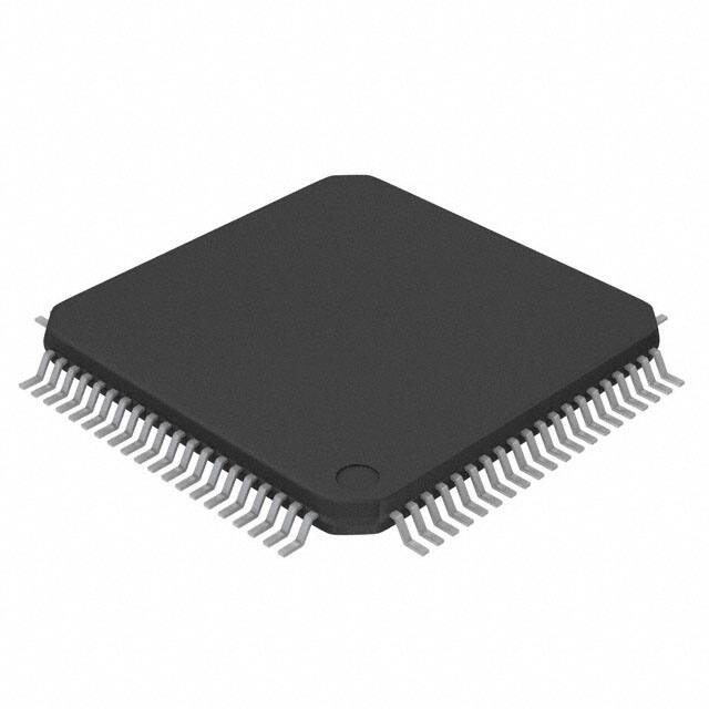


 工商网监
湘ICP备2023018690号
工商网监
湘ICP备2023018690号
