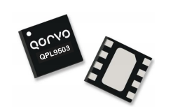
QPL9503
Ultra Low-Noise, Flat Gain LNA
®
General Description
The QPL9503 is a flat-gain, high-linearity, ultra-low noise
amplifier in a small 2 x 2 mm surface-mount package. The
LNA provides a gain flatness of 2 dB (peak-to-peak) over a
wide bandwidth from 3 to 6 GHz. At 5.5 GHz, the amplifier
typically provides 21.6 dB gain, +35.5 dBm OIP3 at a 56mA
bias setting, and 0.95 dB noise figure. The LNA can be
biased from a single positive supply ranging from 3.3 to 5
volts. The device is housed in a green/RoHS-compliant
industry-standard 2x2 mm package.
The QPL9503 is internally matched using a high
performance E-pHEMT process and only requires five
external components for operation from a single positive
supply: an external RF choke and blocking/bypass
capacitors and a bias resistor going to pin 1. This LNA
integrates a shut-down biasing capability to allow for
operation in TDD applications.
The QPL9503 is optimized for linear performance across
the 3 to 6 GHz frequency band but can operate down to 600
MHz.
Functional Block Diagram
Pin 1 Reference Mark
Vbias
1
8
NC
RF In
2
7
RF Out
NC
3
6
GND
GND
4
5
Shut Down
Backside Paddle - RF/DC GND
8 Pin 2X2 mm DFN Package
Product Features
•
•
•
•
•
•
•
•
•
0.6-6 GHz Operational Bandwidth
Ultra low noise figure, 0.95 dB NF @ 5.5 GHz
Bias adjustable for linearity optimization
35.5 dBm OIP3 at 65mA IDD
Shut-down mode pin with 1.8V TTL logic
Unconditionally stable
Integrated shutdown control pin
Maintains OFF state with high Pin drive
+3V to +5V supply; does not require -Vgg
Applications
•
•
•
•
•
•
•
4.5G, 5G Massive MIMO
Repeaters / DAS
Mobile Infrastructure
LTE-U / LAA
L-band, S-band, C-band radios
General Purpose Wireless
TDD or FDD systems
Ordering Information
Top View
Part No.
Description
QPL9503SR
QPL9503TR7
QPL9503EVB-01
100 pcs on 7” reel
2500 pcs on 7” reel
5-6GHz Tuned Evaluation Board
Standard T/R size = 2500 pieces on a 7” reel
Data Sheet April 23, 2018 | Subject to change without notice
1 of 7
www.qorvo.com
�QPL9503
Ultra Low-Noise, Flat Gain LNA
®
Absolute Maximum Ratings
Parameter
Recommended Operating Conditions
Rating
Storage Temperature
Supply Voltage (VDD)
RF Input Power, CW, 50Ω, T=25°C
RF Input Power, WCDMA, 10dB PAR
RF Input Power, CW, OFF State
−65 to 150°C
+7 V
+30 dBm
+27 dBm
+30 dBm
Parameter
Min
Typ
Supply Voltage (VDD)
TCASE
Tj for >106 hours MTTF
3.3
−40
5.0
Max Units
5.25
+105
+190
V
°C
°C
Electrical specifications are measured at specified test
conditions. Specifications are not guaranteed over all
recommended operating conditions.
Operation of this device outside the parameter ranges given
above may cause permanent damage.
Electrical Specifications
Test conditions unless otherwise noted: VDD =+5V, Temp=+25°C, 50 Ω system.
Parameter
Operational Frequency Range
Test Frequency
Gain
Input Return Loss
Output Return Loss
Noise Figure (1)
Output P1dB
Output IP3
Power Shutdown Control (pin 5)
Current, IDD
Shutdown pin current, ISD
Switching Speed
Thermal Resistance, θjc
Conditions
Min
Typ
600
18.5
Pout=+5 dBm/tone, Δf=1 MHz
On state
Off state (Power down)
On state
Off state (Power down)
VPD ≥ 1.17 V
LNA ON to OFF
LNA OFF to ON
channel to case
+30
0
1.17
35
5500
21.6
10
9
0.9
+19
+35.5
56
3
140
20
400
48
Max
Units
6000
MHz
MHz
dB
dB
dB
dB
dBm
dBm
V
V
mA
mA
µA
ns
ns
°C/W
22.5
1.3
0.63
VDD
90
Note:
1) Noise figure data has input trace loss de-embedded.
Data Sheet April 23, 2018 | Subject to change without notice
2 of 7
www.qorvo.com
�QPL9503
Ultra Low-Noise, Flat Gain LNA
®
QPL9503 Evaluation Board
J4 GND
J5
J4
C4
J3
J3 VDD
C5
R
3
1 uF
C3
C5
C4
C8
C1
C2
U1
C9
R4
L1
J1
100 pF
C3
R4
4.3K
J2
100 pF
L1
18 nH
C2
R2
R1
C1
J1
RF
Input
1
2
10 pF
C8
0.2pF
J2
7
Q1
5
5.6 pF
3,4,6,8
C9
0.4pF
RF
Output
R1
0
J6
C6
J5 PD
R2
20K
J7
C7
See notes 4 & 5.
Notes:
1. See Evaluation Board PCB Information section for material and stack-up.
2. R3 (0 Ω jumper) is not shown on the schematic and may be replaced with copper trace in the target application layout.
3. All components are of 0402 size unless stated on the schematic.
4. For TDD Applications: R1 = 20K & R2 = 0Ω
5. For FDD Applications: R1 = 20K ‘OR’ Pin 5 tied to ground. R2 = DNP/Omitted
6. A through line is included on the evaluation board to de-embed the board losses.
7. R4 sets the current draw. Can be changed for the desired bias point.
Bill of Material – QPL9503 Evaluation Board
Reference Des.
N/A
Value
N/A
Description
Printed Circuit Board
Manuf.
Qorvo
Part Number
QPL9503
U1
n/a
Ultra Low Noise, Flat Gain LNA
Qorvo
R4
4.3K
Resistor, Chip, 0402, 5%, 1/16W
various
R2
20K
Resistor, chip, 0402, 5%, 1/16W
various
R1, 3
0Ω
Resistor, Chip, 0402, 5%, 1/16W
various
18 nH
Inductor, 0402, 5%, coil
Coilcraft
0402CS-18NXJL
C1
10 pF
CAP, 0402, +/-1%, 50V
Murata
GJM1555C1H100FB01D
C2
5.6 pF
CAP, 0402, +/-0.1pF, 25V
AVX
C8
0.2 pF
CAP, 0402, +/-0.05pF, 50V
Murata
C9
0.4 pF
CAP, 0402, +/-0.05pF, 50V
AVX
C4
1.0 uF
Cap., Chip, 0402, 10%, 10V, X5R
various
C3, C5, C6, C7
100 pF
Cap., Chip, 0402, 5%, 50V, NPO/COG
various
L1
Data Sheet April 23, 2018 | Subject to change without notice
3 of 7
04023J6R8BBSTR
GJM1555C1HR20WB01
04023J0R4ABSTR
www.qorvo.com
�QPL9503
Ultra Low-Noise, Flat Gain LNA
®
Performance Plots – QPL9503 Evaluation Board
Test conditions unless otherwise noted: VDD=+5 V, IDD = 65mA, Temp=+25°C. Noise figure data has input trace loss de-embedded.
Gain vs. Frequency
25
Input Return Loss vs. Frequency
0
Output Return Loss vs. Frequency
0
+105 °C
+105 °C
+25 °C
+25 °C
22
−40 °C
−40 °C
16
|S22| (dB)
19
-5
|S11| (dB)
Gain (dB)
-5
+105 °C
+25 °C
−40 °C
-10
-10
13
10
1000
2000
3000
4000
5000
6000
-15
1000
7000
2000
3000
Frequency (MHz)
Noise Figure vs Frequency
1.6
4000
5000
6000
-15
1000
7000
2000
3000
Frequency (MHz)
OIP3 vs Pout
38
4000
5000
7000
OIP3 vs Frequency
40
+105 °C
Temp.=+25 °C
+25 °C
37
1.4
6000
Frequency (MHz)
36
−40 °C
37
1.0
0.8
0.6
OIP3 (dBm)
35
OIP3 (dBm)
Noise Figure (dB)
1.2
34
33
32
31
3GHz
4GHz
4.5GHz
5GHz
5.5GHz
6GHz
0.4
30
0.2
29
0.0
3.5
4
4.5
5
5.5
6
25
-3
-2
-1
0
Frequency (GHz)
1
2
3
4
5
6
7
3
Pout/tone (dBm)
P1dB vs Frequency
25
31
28
28
3
34
4
4.5
5
5.5
6
Frequency (GHz)
Gain & IDD vs Pin (LNA OFF)
-5
3.5
40
VPD = 1.2V
+105 °C
-10
35
-15
30
-20
25
-25
20
-30
15
−40 °C
Gain (dB)
P1dB (dBm)
20
15
-35
IDD (mA)
+25 °C
10
-40
5
Gain
IDD
-45
10
3
3.5
4
4.5
5
5.5
6
0
-10
-5
0
5
10
Frequency (GHz)
Pin (dBm)
Data Sheet April 23, 2018 | Subject to change without notice
4 of 7
15
20
25
www.qorvo.com
�QPL9503
Ultra Low-Noise, Flat Gain LNA
®
Pin Configuration and Description
Pin 1 Reference Mark
Vbias
1
8
NC
RF In
2
7
RF Out
NC
3
6
GND
GND
4
5
Shut Down
Backside Paddle - RF/DC GND
Pin No.
Label
Description
1
Vbias
Sets the Icq bias point for the device.
2
RF In
5
Shut Down
7
RF Out / DCBias
3 ,8
Backside
Paddle, 4, 6
NC
RF Input pin. A DC Block is required.
A high voltage(>1.17V) turns off the device. If the pin is pulled to ground or driven
with a voltage less than 0.63V, then the device will operate under LNA ON state.
RF Output pin. DC bias will also need to be injected through a RF bias
choke/inductor for operation.
No electrical connection. Provide grounded land pads for PCB mounting integrity.
RF/DC ground. Use recommended via pattern to minimize inductance and thermal
resistance; see PCB Mounting Pattern for suggested footprint.
RF/DC GND
Evaluation Board PCB Information
Qorvo PCB 281645 Material and Stack-up
0.008"
0.062" ± 0.006"
Finished Board
Thickness
Rogers 4003C
εr=3.5 typ.
1 oz. Cu top layer
1 oz. Cu inner layer
FR4
1 oz. Cu inner layer
0.008"
FR4
1 oz. Cu bottom layer
50 ohm line dimensions: width = 0.0182”, spacing = 0.020”
Data Sheet April 23, 2018 | Subject to change without notice
5 of 7
www.qorvo.com
�QPL9503
Ultra Low-Noise, Flat Gain LNA
®
Mechanical Information
Package Marking and Dimensions
9503
Trace Code
Notes:
1. All dimensions are in millimeters. Angles are in degrees.
2. Except where noted, this part outline conforms to JEDEC standard MO-220, Issue E (Variation VGGC) for thermally enhanced
plastic very thin fine pitch quad flat no lead package (QFN).
3. Dimension and tolerance formats conform to ASME Y14.4M-1994.
4. The terminal #1 identifier and terminal numbering conform to JESD 95-1 SPP-012.
PCB Mounting Pattern
Notes:
1. All dimensions are in millimeters. Angles are in degrees.
2. Use 1 oz. copper minimum for top and bottom layer metal.
3. Vias are required under the backside paddle of this device for proper RF/DC grounding and thermal dissipation. We recommend
a 0.35mm (#80/.0135") diameter bit for drilling via holes and a final plated thru diameter of 0.25 mm (0.10”).
4. Ensure good package backside paddle solder attach for reliable operation and best electrical performance.
Data Sheet April 23, 2018 | Subject to change without notice
6 of 7
www.qorvo.com
�QPL9503
Ultra Low-Noise, Flat Gain LNA
®
Handling Precautions
Parameter
Rating
Standard
ESD – Human Body Model (HBM)
1C
ESDA / JEDEC JS-001-2014
ESD – Charged Device Model (CDM)
C3
ESDA / JEDEC JS-002-2014
MSL – Moisture Sensitivity Level
Level 1
IPC/JEDEC J-STD-020
Caution!
ESD-Sensitive Device
Solderability
Compatible with lead-free (260°C max. reflow temp.) soldering process.
Solder profiles available upon request.
Contact plating: NiPdAu
RoHS Compliance
This part is compliant with 2011/65/EU RoHS directive (Restrictions on the Use of Certain Hazardous Substances in Electrical and
Electronic Equipment) as amended by Directive 2015/863/EU.
This product also has the following attributes:
• Lead Free
• Halogen Free (Chlorine, Bromine)
• Antimony Free
• TBBP-A (C15H12Br402) Free
• PFOS Free
• SVHC Free
Pb
Contact Information
For the latest specifications, additional product information, worldwide sales and distribution locations:
Web: www.qorvo.com
Tel: 1-844-890-8163
Email: customer.support@qorvo.com
For technical questions and application information:
Email:
appsupport@qorvo.com
Important Notice
The information contained herein is believed to be reliable; however, Qorvo makes no warranties regarding the information contained
herein and assumes no responsibility or liability whatsoever for the use of the information contained herein. All information contained
herein is subject to change without notice. Customers should obtain and verify the latest relevant information before placing orders for
Qorvo products. The information contained herein or any use of such information does not grant, explicitly or implicitly, to any party any
patent rights, licenses, or any other intellectual property rights, whether with regard to such information itself or anything described by
such information. THIS INFORMATION DOES NOT CONSTITUTE A WARRANTY WITH RESPECT TO THE PRODUCTS DESCRIBED
HEREIN, AND QORVO HEREBY DISCLAIMS ANY AND ALL WARRANTIES WITH RESPECT TO SUCH PRODUCTS WHETHER
EXPRESS OR IMPLIED BY LAW, COURSE OF DEALING, COURSE OF PERFORMANCE, USAGE OF TRADE OR OTHERWISE,
INCLUDING THE IMPLIED WARRANTIES OF MERCHANTABILITY AND FITNESS FOR A PARTICULAR PURPOSE.
Without limiting the generality of the foregoing, Qorvo products are not warranted or authorized for use as critical components in medical,
life-saving, or life-sustaining applications, or other applications where a failure would reasonably be expected to cause severe personal
injury or death.
Copyright 2018 © Qorvo, Inc. | Qorvo is a registered trademark of Qorvo, Inc.
Data Sheet April 23, 2018 | Subject to change without notice
7 of 7
www.qorvo.com
�