HMC576LC3B
v02.0514
MULTIPLIERS - ACTIVE - SMT
SMT GaAs MMIC x2 ACTIVE FREQUENCY
MULTIPLIER, 18 - 29 GHz OUTPUT
Typical Applications
Features
The HMC576LC3B is suitable for:
High Output Power: +15 dBm
• Clock Generation Applications:
SONET OC-192 & SDH STM-64
Low Input Power Drive: 0 to +6 dBm
• Point-to-Point & VSAT Radios
Fo Isolation: >20 dBc @ Fout= 24 GHz
100 KHz SSB Phase Noise: -132 dBc/Hz
• Test Instrumentation
Single Supply: +5V@ 82 mA
• Military & Space
RoHS Compliant 3x3 mm SMT Package
Functional Diagram
General Description
The HMC576LC3B is a x2 active broadband frequency multiplier utilizing GaAs PHEMT technology in a
leadless RoHS compliant SMT package. When driven
by a +3 dBm signal, the multiplier provides +15 dBm
typical output power from 18 to 29 GHz. The Fo and
3Fo isolations are >20 dBc at 24 GHz. The
HMC576LC3B is ideal for use in LO multiplier chains
for Pt-to-Pt & VSAT Radios yielding reduced parts
count vs. traditional approaches. The low additive
SSB Phase Noise of -132 dBc/Hz at 100 kHz offset
helps maintain good system noise performance. The
RoHS packaged HMC576LC3B eliminates the need
for wire bonding, and allows the use of surface mount
manufacturing techniques.
Electrical Specifications, TA = +25° C, Vdd1, Vdd2 = +5V, 3 dBm Drive Level
Parameter
Min.
Frequency Range, Input
Frequency Range, Output
Max.
Units
GHz
18 - 29
GHz
15
dBm
Fo Isolation (with respect to output level)
20
dBc
3Fo Isolation (with respect to output level)
20
dBc
Input Return Loss
10
dB
Output Return Loss
10
dB
-132
dBc/Hz
82
mA
Output Power
SSB Phase Noise (100 kHz Offset)
Supply Current (Idd1 & Idd2)
1
Typ.
9 - 14.5
10
Information furnished by Analog Devices is believed to be accurate and reliable. However, no
For price, 2delivery,
and to
placeChelmsford,
orders: Analog MA
Devices,
Inc.,
For price,
delivery
and
to place
orders:
Microwave
Corporation,
Elizabeth
Drive,
01824
responsibility
is assumed
by Analog
Devices
for its use,
nor for anyHittite
infringements
of patents or other
One Technology Way, P.O. Box 9106, Norwood, MA 02062-9106
rights of third parties that may result from its use. Specifications subject to change without notice. No
Phone: 978-250-3343
Fax: 978-250-3373 Phone:
Order781-329-4700
On-line at www.hittite.com
• Order online at www.analog.com
license is granted by implication or otherwise under any patent or patent rights of Analog Devices.
Application
Support: Phone: 1-800-ANALOG-D
Trademarks and registered trademarks are
the property of their
respective owners.
Application
Support:
Phone: 978-250-3343
or apps@hittite.com
�HMC576LC3B
v02.0514
SMT GaAs MMIC x2 ACTIVE FREQUENCY
MULTIPLIER, 18 - 29 GHz OUTPUT
20
25
18
20
16
15
14
12
10
8
+25C
+85C
-40C
6
4
10
5
0
-5
-10
-15
-6 dBm
-4 dBm
-2 dBm
0 dBm
-20
2
-25
0
2 dBm
4 dBm
6 dBm
-30
17
18 19 20
21 22 23
24
25 26 27
28 29
30
17
18 19 20
21 22 23
FREQUENCY (GHz)
24
25 26 27
28 29
30
28 29
30
FREQUENCY (GHz)
Output Power vs.
Supply Voltage @ 3 dBm Drive Level
Isolation @ 3 dBm Drive Level
20
20
16
OUTPUT POWER (dBm)
OUTPUT POWER (dBm)
18
14
12
10
8
4.5V
5.0V
5.5V
6
4
10
0
-10
Fo
2Fo
3Fo
-20
2
0
MULTIPLIERS - ACTIVE - SMT
Output Power vs. Drive Level
OUTPUT POWER (dBm)
OUTPUT POWER (dBm)
Output Power vs.
Temperature @ 3 dBm Drive Level
-30
17
18 19 20
21 22 23
24
25 26 27
28 29
17
30
18 19 20
21 22 23
FREQUENCY (GHz)
24
25 26 27
FREQUENCY (GHz)
Output Power vs. Input Power
20
OUTPUT POWER (dBm)
15
10
5
0
-5
18GHz
24GHz
29GHz
-10
-15
-20
-10
-8
-6
-4
-2
0
2
4
6
8
10
INPUT POWER (dBm)
Information furnished by Analog Devices is believed to be accurate and reliable. However, no
For price, 2delivery,
and to
placeChelmsford,
orders: Analog MA
Devices,
Inc.,
For price,
delivery
and
to place
orders:
Microwave
Corporation,
Elizabeth
Drive,
01824
responsibility
is assumed
by Analog
Devices
for its use,
nor for anyHittite
infringements
of patents or other
One Technology Way, P.O. Box 9106, Norwood, MA 02062-9106
rights of third parties that may result from its use. Specifications subject to change without notice. No
Phone: 978-250-3343
Fax: 978-250-3373 Phone:
Order781-329-4700
On-line at www.hittite.com
• Order online at www.analog.com
license is granted by implication or otherwise under any patent or patent rights of Analog Devices.
Application
Support: Phone: 1-800-ANALOG-D
Trademarks and registered trademarks are
the property of their
respective owners.
Application
Support:
Phone: 978-250-3343
or apps@hittite.com
2
�HMC576LC3B
v02.0514
SMT GaAs MMIC x2 ACTIVE FREQUENCY
MULTIPLIER, 18 - 29 GHz OUTPUT
Input Return Loss vs. Temperature
Output Return Loss vs. Temperature
0
3
OUTPUT RETURN LOSS (dB)
INPUT RETURN LOSS (dB)
MULTIPLIERS - ACTIVE - SMT
0
-5
-10
-15
-20
+25C
+85C
-40C
-25
-30
+25C
+85C
-40C
-5
-10
-15
-20
-25
8
9
10
11
12
FREQUENCY (GHz)
13
14
15
17
18 19 20
21 22 23
24
25 26 27
28 29
30
FREQUENCY (GHz)
Information furnished by Analog Devices is believed to be accurate and reliable. However, no
For price, 2delivery,
and to
placeChelmsford,
orders: Analog MA
Devices,
Inc.,
For price,
delivery
and
to place
orders:
Microwave
Corporation,
Elizabeth
Drive,
01824
responsibility
is assumed
by Analog
Devices
for its use,
nor for anyHittite
infringements
of patents or other
One Technology Way, P.O. Box 9106, Norwood, MA 02062-9106
rights of third parties that may result from its use. Specifications subject to change without notice. No
Phone: 978-250-3343
Fax: 978-250-3373 Phone:
Order781-329-4700
On-line at www.hittite.com
• Order online at www.analog.com
license is granted by implication or otherwise under any patent or patent rights of Analog Devices.
Application
Support: Phone: 1-800-ANALOG-D
Trademarks and registered trademarks are
the property of their
respective owners.
Application
Support:
Phone: 978-250-3343
or apps@hittite.com
�HMC576LC3B
v02.0514
SMT GaAs MMIC x2 ACTIVE FREQUENCY
MULTIPLIER, 18 - 29 GHz OUTPUT
Typical Supply Current vs. Vdd
RF Input (Vdd = +5V)
+13 dBm
Vdd (Vdc)
Idd (mA)
Supply Voltage (Vdd)
+6.0 Vdc
4.5
82
Channel Temperature
175 °C
Continuous Pdiss (T= 85 °C)
(derate 7.5 mW/°C above 85 °C)
676 mW
Thermal Resistance
(channel to ground paddle)
133 °C/W
Storage Temperature
-65 to +150 °C
Operating Temperature
-40 to +85 °C
5.0
82
5.5
83
Note:
Multiplier will operate over full voltage range shown above.
ELECTROSTATIC SENSITIVE DEVICE
OBSERVE HANDLING PRECAUTIONS
Outline Drawing
MULTIPLIERS - ACTIVE - SMT
Absolute Maximum Ratings
NOTES:
1. PACKAGE BODY MATERIAL: ALUMINA
2. LEAD AND GROUND PADDLE PLATING: 30-80 MICROINCHES GOLD OVER
50 MICROINCHES MINIMUM NICKEL.
3. DIMENSIONS ARE IN INCHES [MILLIMETERS].
4. LEAD SPACING TOLERANCE IS NON-CUMULATIVE
5. PACKAGE WARP SHALL NOT EXCEED 0.05mm DATUM -C6. ALL GROUND LEADS AND GROUND PADDLE MUST BE SOLDERED
TO PCB RF GROUND.
Package Information
Part Number
Package Body Material
Lead Finish
HMC576LC3B
Alumina, White
Gold over Nickel
MSL Rating
MSL3
[1]
Package Marking [2]
H576
XXXX
[1] Max peak reflow temperature of 260 °C
[2] 4-Digit lot number XXXX
Information furnished by Analog Devices is believed to be accurate and reliable. However, no
For price, 2delivery,
and to
placeChelmsford,
orders: Analog MA
Devices,
Inc.,
For price,
delivery
and
to place
orders:
Microwave
Corporation,
Elizabeth
Drive,
01824
responsibility
is assumed
by Analog
Devices
for its use,
nor for anyHittite
infringements
of patents or other
One Technology Way, P.O. Box 9106, Norwood, MA 02062-9106
rights of third parties that may result from its use. Specifications subject to change without notice. No
Phone: 978-250-3343
Fax: 978-250-3373 Phone:
Order781-329-4700
On-line at www.hittite.com
• Order online at www.analog.com
license is granted by implication or otherwise under any patent or patent rights of Analog Devices.
Application
Support: Phone: 1-800-ANALOG-D
Trademarks and registered trademarks are
the property of their
respective owners.
Application
Support:
Phone: 978-250-3343
or apps@hittite.com
4
�HMC576LC3B
v02.0514
SMT GaAs MMIC x2 ACTIVE FREQUENCY
MULTIPLIER, 18 - 29 GHz OUTPUT
MULTIPLIERS - ACTIVE - SMT
Pin Description
5
Pin Number
Function
Description
1, 3, 7, 9
GND
Package bottom must also be connected
to RF/DC ground.
2
RFIN
Pin is AC coupled
and matched to 50 Ohms.
4 - 6, 11
N/C
These pins are internally not connected; however,
this product was specified with these pins connected
to RF/ DC ground.
8
RFOUT
Pin is AC coupled
and matched to 50 Ohms.
10, 12
Vdd2, Vdd1
Supply voltage 5V ± 0.5V. External bypass capacitors
of 100 pF, 1,000 pF and 2.2 µF are required.
Interface Schematic
Application Circuit
Component
Value
C1, C2
100 pF
C3, C4
1,000 pF
C5, C6
2.2 µF
Information furnished by Analog Devices is believed to be accurate and reliable. However, no
For price, 2delivery,
and to
placeChelmsford,
orders: Analog MA
Devices,
Inc.,
For price,
delivery
and
to place
orders:
Microwave
Corporation,
Elizabeth
Drive,
01824
responsibility
is assumed
by Analog
Devices
for its use,
nor for anyHittite
infringements
of patents or other
One Technology Way, P.O. Box 9106, Norwood, MA 02062-9106
rights of third parties that may result from its use. Specifications subject to change without notice. No
Phone: 978-250-3343
Fax: 978-250-3373 Phone:
Order781-329-4700
On-line at www.hittite.com
• Order online at www.analog.com
license is granted by implication or otherwise under any patent or patent rights of Analog Devices.
Application
Support: Phone: 1-800-ANALOG-D
Trademarks and registered trademarks are
the property of their
respective owners.
Application
Support:
Phone: 978-250-3343
or apps@hittite.com
�HMC576LC3B
v02.0514
SMT GaAs MMIC x2 ACTIVE FREQUENCY
MULTIPLIER, 18 - 29 GHz OUTPUT
MULTIPLIERS - ACTIVE - SMT
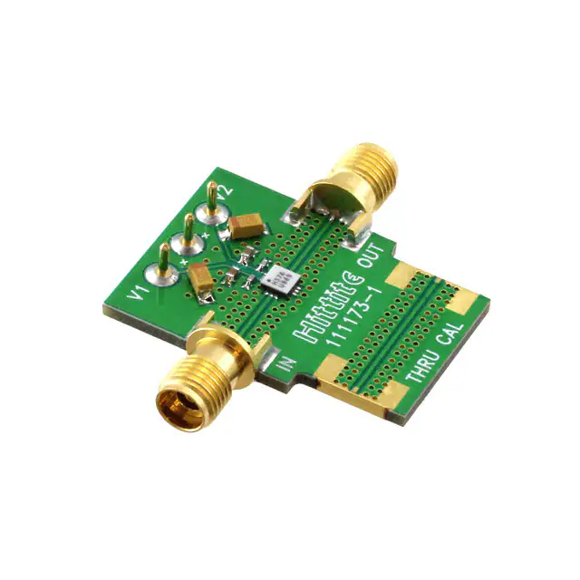
Evaluation PCB
List of Materials for Evaluation PCB 112409 [1]
Item
Description
J1, J2
PCB Mount SRI K Connector
J3 - J5
DC Pin
C1, C2
100 pF Capacitor, 0402 Pkg.
C3, C4
1,000 pF Capacitor, 0603 Pkg.
C5, C6
2.2 µF Tantalum Capacitor
U1
HMC576LC3B x2 Active Multiplier
PCB [2]
111173 Eval Board
[1] Reference this number when ordering complete evaluation PCB
[2] Circuit Board Material: Rogers 4350
The circuit board used in the final application
should be generated with proper RF circuit design
techniques. Signal lines should have 50 ohm
impedance while the package ground leads and
exposed paddle should be connected directly to
the ground plane similar to that shown. A sufficient
number of via holes should be used to connect
the top and bottom ground planes. The evaluation
circuit board shown is available from Hittite upon
request.
Information furnished by Analog Devices is believed to be accurate and reliable. However, no
For price, 2delivery,
and to
placeChelmsford,
orders: Analog MA
Devices,
Inc.,
For price,
delivery
and
to place
orders:
Microwave
Corporation,
Elizabeth
Drive,
01824
responsibility
is assumed
by Analog
Devices
for its use,
nor for anyHittite
infringements
of patents or other
One Technology Way, P.O. Box 9106, Norwood, MA 02062-9106
rights of third parties that may result from its use. Specifications subject to change without notice. No
Phone: 978-250-3343
Fax: 978-250-3373 Phone:
Order781-329-4700
On-line at www.hittite.com
• Order online at www.analog.com
license is granted by implication or otherwise under any patent or patent rights of Analog Devices.
Application
Support: Phone: 1-800-ANALOG-D
Trademarks and registered trademarks are
the property of their
respective owners.
Application
Support:
Phone: 978-250-3343
or apps@hittite.com
6
�