HMC601LP4 / 601LP4E
v01.0509
75 dB, FAST SETTLING, LOGARITHMIC
DETECTOR / CONTROLLER 10 - 4000 MHz
Typical Applications
Features
The HMC601LP4(E) is ideal for IF and RF
applications in:
Wide Dynamic Range: up to 75 dB
• Cellular/PCS/3G
Flexible Supply Voltage: +2.7V to +5.5V
• WiMAX, WiBro & Fixed Wireless
Power-Down Mode
• Power Monitoring & Control Circuitry
Excellent Stability over Temperature
• Receiver Signal Strength Indication (RSSI)
Compact 4x4mm Leadless SMT Package
Fast Pulse Response: 15/34ns (Rise/Fall Time)
• Automatic Gain & Power Control Circuits
POWER DETECTORS - SMT
12
Functional Diagram
General Description
The HMC601LP4(E) Logarithmic Detector/Controller
converts RF signals at its input, to a proportional DC
voltage at its output. The HMC601LP4(E) employ
a successive compression topology which delivers
extremely high dynamic range and conversion
accuracy over a wide input frequency range. As
the input power is increased, successive amplifiers
move into saturation one by one creating an accurate
approximation of the logarithm function. The output of
a series of square law detectors is summed, converted
into voltage domain and buffered to drive the LOGOUT
output. For detection mode, the LOGOUT pin is
shorted to the VSET input, and will provide a nominal
logarithmic slope of 19mV/dB and an intercept of
-100dBm. The HMC601LP4(E) can also be used in the
controller mode where an external voltage is applied to
the VSET pin, to create an AGC or APC feedback loop.
The HMC601LP4(E) provides a 15/34ns (rise/fall time)
response time enabling RF burst detection to a pulse
rate beyond 20 MHz.
Electrical Specifi cations, TA = +25C, PWD = 0V, Vcc1, Vcc2 = +3.3V [1]
Parameter
Input Frequency
Typ.
Typ.
Typ.
Typ.
Typ.
Typ.
Typ.
Typ.
Units
50
100
500
900
1900
2500
3500
4000
MHz
±3 dB Dynamic Range
74
74
74
74
70
68
54
52
dB
±3 dB Dynamic Range Center
-31
-31
-31
-31
-31.5
-31.5
-27
-23
dBm
±1 dB Dynamic Range
Output Slope
Output Intercept
Temperature Sensitivity @ -10 dBm Input
[2]
68
68
69
69
67
65
47
46
dB
19.5
19.4
19.2
19.1
19.0
19.4
20.9
19.6
mV/dB
-99
-99
-100
-100
-98
-96
-85
-79
dBm
-4.2
-3.8
-3.5
-2.4
-0.8
-0.8
-4.4
-3.5
mdB/°C
[1] Detector mode measurements; LOGOUT (Pin 17) is shorted to VSET (Pin 16).
[2] Measured from TA = -40C to TA = +85C
Parameter
Conditions
Min.
Typ.
Max.
Units
RF Input (INP)
Return Loss
F = 10 - 4000 MHz, Zo = 50Ω, See plot
10
dB
(Simulated)
12
kΩ
LOGOUT Interface
Open Loop Impedance
12 - 10
For price,
delivery,
and to place
orders: Analog Devices, Inc.,
For price, delivery, and to place orders, please contact
Hittite
Microwave
Corporation:
One Technology Way, P.O. Box 9106, Norwood, MA 02062-9106
20 Alpha Road, Chelmsford, MA 01824 Phone: 978-250-3343
Fax:
978-250-3373
Phone: 781-329-4700
• Order
online at www.analog.com
Application Support: Phone: 1-800-ANALOG-D
Order On-line at www.hittite.com
Information furnished by Analog Devices is believed to be accurate and reliable. However, no
responsibility is assumed by Analog Devices for its use, nor for any infringements of patents or other
rights of third parties that may result from its use. Specifications subject to change without notice. No
license is granted by implication or otherwise under any patent or patent rights of Analog Devices.
Trademarks and registered trademarks are the property of their respective owners.
�HMC601LP4 / 601LP4E
v01.0509
75 dB, FAST SETTLING, LOGARITHMIC
DETECTOR / CONTROLLER 10 - 4000 MHz
Electrical Specifi cations, (continued)
Parameter
Conditions
Min.
Typ.
Current Drive (Source)
Max.
Units
0.55
Current Drive (Sink)
For 1% change in the output voltage
mA
4.8
Output Voltage Range
mA
0
Small Signal Response Time (10% to 90%)
Large Signal Response Time (±0.5 dB Settling)
Vcc -0.13
V
Pin = -60 to -57 dBm
8
ns
Pin = No Signal to 0 dBm
50
ns
Output Rise Time
Ripple
From 0% to 90%
15
ns
Fin = 100 MHz
0.8xVcc to initiate a
power saving shutdown mode.
14
PWD
16
VSET
VSET input in controller mode. Short this
pin to LOGOUT for detector mode.
17
LOGOUT
Logarithmic output that converts the input power
to a DC level in detector mode. Short this pin to
VSET for detector mode.
Package
Base
GND
Exposed paddle must be connected to RF and DC ground.
POWER DETECTORS - SMT
Pin Number
To ensure proper start-up apply the power-up sequence
shown in the “Power-Up Timing Diagram” attached to the
application circuit.
For price,
delivery,
and to place
orders: Analog Devices, Inc.,
For price, delivery, and to place orders, please contact
Hittite
Microwave
Corporation:
One Technology Way, P.O. Box 9106, Norwood, MA 02062-9106
20 Alpha Road, Chelmsford, MA 01824 Phone: 978-250-3343
Fax:
978-250-3373
Phone: 781-329-4700
• Order
online at www.analog.com
Application Support: Phone: 1-800-ANALOG-D
Order On-line at www.hittite.com
Information furnished by Analog Devices is believed to be accurate and reliable. However, no
responsibility is assumed by Analog Devices for its use, nor for any infringements of patents or other
rights of third parties that may result from its use. Specifications subject to change without notice. No
license is granted by implication or otherwise under any patent or patent rights of Analog Devices.
Trademarks and registered trademarks are the property of their respective owners.
12 - 15
�HMC601LP4 / 601LP4E
v01.0509
75 dB, FAST SETTLING, LOGARITHMIC
DETECTOR / CONTROLLER 10 - 4000 MHz
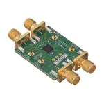
Evaluation PCB
POWER DETECTORS - SMT
12
List of Materials for Evaluation PCB 115242 [1]
Item
Description
J1 - J4
PC Mount SMA Connector
J5 - J8
DC Pin
C1, C2
1000 pF Capacitor, 0402 Pkg.
C3, C4
0.1μF Capacitor, 0402 Pkg.
R1, R2
5.6Ω Resistor, 0603 Pkg.
R3-R5
0Ω Resistor, 0603 Pkg.
U1
HMC601LP4 / HMC601LP4E
Logarithmic Detector / Controller
PCB [2]
115244 Evaluation PCB
The circuit board used in the final application should
use RF circuit design techniques. Signal lines
should have 50 ohm impedance while the package
ground leads and exposed paddle should be connected directly to the ground plane similar to that
shown. A sufficient number of via holes should be
used to connect the top and bottom ground planes.
The evaluation circuit board shown is available from
Hittite upon request.
[1] Reference this number when ordering complete evaluation PCB
[2] Circuit Board Material: Rogers 4350
12 - 16
For price,
delivery,
and to place
orders: Analog Devices, Inc.,
For price, delivery, and to place orders, please contact
Hittite
Microwave
Corporation:
One Technology Way, P.O. Box 9106, Norwood, MA 02062-9106
20 Alpha Road, Chelmsford, MA 01824 Phone: 978-250-3343
Fax:
978-250-3373
Phone: 781-329-4700
• Order
online at www.analog.com
Application Support: Phone: 1-800-ANALOG-D
Order On-line at www.hittite.com
Information furnished by Analog Devices is believed to be accurate and reliable. However, no
responsibility is assumed by Analog Devices for its use, nor for any infringements of patents or other
rights of third parties that may result from its use. Specifications subject to change without notice. No
license is granted by implication or otherwise under any patent or patent rights of Analog Devices.
Trademarks and registered trademarks are the property of their respective owners.
�HMC601LP4 / 601LP4E
v01.0509
75 dB, FAST SETTLING, LOGARITHMIC
DETECTOR / CONTROLLER 10 - 4000 MHz
Application & Evaluation PCB Schematic
Notes
Note 1: The HMC601LP4 & HMC601LP4E evaluation boards are pre-assembled for single-ended input, and detector/RSSI mode.
Note 2: For single-ended input operation, use the INP port and make no connection to INN. INN is AC coupled to ground by C2
Note 3: For differential input, remove C2, and install a 1000pF capacitor in series with INN at location shown.
Note 4: For detector mode, connect high impedence volt meter to the LOGOUT port, and make no connection to VSET. LOGOUT
is shorted to VSET by R3, as required for detector mode.
Note 5: For controller mode, remove R3 and make appropriate connection to LOGOUT and VSET. In controller mode, the
LOGOUT output can be used to drive a variable gain amplifier, or a variable attenuator, either directly or through a buffer
or microcontroller. VSET should be connected to an external supply, typically between +0.6 and +1.9V.
Power-Up Timing Diagram
For price,
delivery,
and to place
orders: Analog Devices, Inc.,
For price, delivery, and to place orders, please contact
Hittite
Microwave
Corporation:
One Technology Way, P.O. Box 9106, Norwood, MA 02062-9106
20 Alpha Road, Chelmsford, MA 01824 Phone: 978-250-3343
Fax:
978-250-3373
Phone: 781-329-4700
• Order
online at www.analog.com
Application Support: Phone: 1-800-ANALOG-D
Order On-line at www.hittite.com
Information furnished by Analog Devices is believed to be accurate and reliable. However, no
responsibility is assumed by Analog Devices for its use, nor for any infringements of patents or other
rights of third parties that may result from its use. Specifications subject to change without notice. No
license is granted by implication or otherwise under any patent or patent rights of Analog Devices.
Trademarks and registered trademarks are the property of their respective owners.
POWER DETECTORS - SMT
12
12 - 17
�