HMC615LP4 / 615LP4E
v03.0412
Features
The HMC615LP4E is ideal for:
High Input IP3: +35 dBm
• PCS / 3G Infrastructure
Low Input LO Drive: -2 to +6 dBm
• Base Stations & Repeaters
Low Conversion Loss: 10 dB
• WiMAX & WiBro
Single Positive Supply: +5V @ 65 mA
• ISM & Fixed Wireless
24 Lead 4x4mm QFN Package: 9 mm²
Functional Diagram
General Description
TE
Typical Applications
LE
The HMC615LP4(E) are high linearity, GaAs FET
converter ICs that operate from 2.3 to 4.0 GHz and
deliver a +35 dBm input third order intercept point.
The LO amplifier output and high dynamic range
mixer input are positioned so that an external LO
filter can be placed in series between them. The IC
operates from a single +5V supply consuming 65
mA of current and accepts a LO drive level of -2 to
+6 dBm. The design requires no external baluns and
supports IF frequencies between DC and 1 GHz.
The HMC615LP4(E) is pin for pin compatible with the
HMC551LP4(E), HMC552LP4(E) and HMC215LP4(E),
which operate from 0.8 to 4.0 GHz. For availability
on Non-RoHS HMC615LP4 products please contact
Hittite Microwave sales directly.
B
SO
Mixers - High IP3 - SMT
GaAs MMIC MIXER w/ INTEGRATED
LO AMPLIFIER, 2.3 - 4.0 GHz
O
Electrical Specifications, TA = +25° C, LO = 4 dBm, Vcc = +5V, R1 = 18 Ohms, IF = 200 MHz*
Parameter
Min.
Typ.
Frequency Range, RF, LO
2.3 - 4.0
Frequency Range, IF
DC - 1.0
Conversion Loss *
10
Noise Figure (SSB)
10
Max.
Units
GHz
GHz
13
dB
dB
LO to RF Isolation
5
15
dB
LO to IF Isolation *
1
10
dB
IP3 (Input)
35
dBm
1 dB Compression (Input)
21
dBm
LO Drive Input Level (Typical)
Supply Current (Icc)
-2 to +6
65
dBm
75
mA
*Unless otherwise noted, all measurements performed as a downconverter configured as shown in application circuit.
1
Information
furnished
by Analog
Devices
is believed
to be accurate
andMicrowave
reliable. However,
no
For price,2 delivery,
andDrive,
to placeChelmsford,
orders: AnalogMA
Devices,
For price,
delivery
and
to place
orders:
Hittite
Corporation,
Elizabeth
01824Inc.,
responsibility is assumed by Analog Devices for its use, nor for any infringements of patents or other
One Technology Way, P.O. Box 9106, Norwood, MA 02062-9106
rights of third parties that may
result
from
its
use.
Specifications
subject
to
change
without
notice.
No
Phone: 978-250-3343
Fax: 978-250-3373
Order
at www.hittite.com
Phone: On-line
781-329-4700
• Order online at www.analog.com
license is granted by implication or otherwise under any patent or patent rights of Analog Devices.
Application
Support: Phone: 1-800-ANALOG-D
Trademarks and registered trademarks are
the property of their
respective owners.
Application
Support:
Phone: 978-250-3343
or apps@hittite.com
�HMC615LP4 / 615LP4E
v03.0412
v02.1210
GaAs MMIC MIXER w/ INTEGRATED
LO AMPLIFIER, 2.3 - 4.0 GHz
Conversion Gain
vs. Temperature @ LO = 4 dBm
Isolation @ LO = 4 dBm
-5
+25C
+85C
-40C
-5
-15
RF to IF
LO to RF
LO to IF
-20
TE
-10
-10
-15
-25
2
2.5
3
3.5
4
-30
1.5
4.5
Conversion Gain vs. LO Drive
-15
-20
1.5
LO= -4 dBm
LO= -2 dBm
LO= 0 dBm
LO= 2 dBm
LO= 4 dBm
LO= 6 dBm
4
4.5
4
4.5
-5
2
2.5
3
3.5
4
-10
-15
-20
LO
RF
-25
-30
1.5
4.5
O
Upconverter Performance (IF= 100 MHz)
Conversion Gain vs. LO Drive
2
2.5
3
3.5
FREQUENCY (GHz)
IF Bandwidth @ LO = 4 dBm
0
0
LO= -4 dBm
LO= -2 dBm
LO= 0 dBm
LO= 2 dBm
LO= 4 dBm
LO= 6 dBm
-5
Conversion Gain
Return Loss
-5
RESPONSE (dB)
CONVERSION GAIN (dB)
3.5
Return Loss @ LO = 4 dBm
FREQUENCY (GHz)
-10
-15
-20
1.5
3
0
-5
-10
2.5
FREQUENCY (GHz)
B
SO
CONVERSION GAIN (dB)
0
2
LE
FREQUENCY (GHz)
RETURN LOSS (dB)
-20
1.5
Mixers - High IP3 - SMT
0
ISOLATION (dB)
CONVERSION GAIN (dB)
0
-10
-15
-20
-25
2
2.5
3
3.5
FREQUENCY (GHz)
4
4.5
0
0.5
1
1.5
2
2.5
FREQUENCY (GHz)
Information furnished by Analog Devices is believed to be accurate and reliable. However, no
For price, 2delivery,
and to
place Chelmsford,
orders: Analog MA
Devices,
Inc.,
For price,
delivery
and
to place
orders:
Microwave
Corporation,
Elizabeth
Drive,
01824
responsibility
is assumed
by Analog
Devices
for its use,
nor for anyHittite
infringements
of patents or other
One Technology Way, P.O. Box 9106, Norwood, MA 02062-9106
rights of third parties that mayPhone:
result from 978-250-3343
its use. Specifications subject
to
change
without
notice.
No
Fax: 978-250-3373 Phone:
Order781-329-4700
On-line at www.hittite.com
• Order online at www.analog.com
license is granted by implication or otherwise under any patent or patent rights of Analog Devices.
Application
Support: Phone: 1-800-ANALOG-D
Trademarks and registered trademarks areApplication
the property of their
respective owners.
Support:
Phone: 978-250-3343
or apps@hittite.com
2
�HMC615LP4 / 615LP4E
v03.0412
GaAs MMIC MIXER w/ INTEGRATED
LO AMPLIFIER, 2.3 - 4.0 GHz
40
40
30
30
IP3 (dBm)
50
0
1.8
2.2
2.6
3
3.4
3.8
0
1.8
4.2
3.8
4.2
3.8
4.2
B
SO
40
+ 25C
+ 85C
- 40C
2.2
2.6
3
3.4
3.8
30
20
LO= -2 dBm
LO= 0 dBm
LO= 2 dBm
LO= 4 dBm
LO= 6 dBm
10
0
1.8
4.2
O
Input P1dB vs. Temperature @ LO = 4 dBm
2.2
2.6
20
+25C
+85C
-40C
2.1
2.5
2.9
3.4
MxN Spurious @ IF Port
nLO
25
15
3
FREQUENCY (GHz)
30
P1dB (dBm)
3.4
Input IP2 vs. LO Drive
FREQUENCY (GHz)
10
1.7
3
50
40
0
1.8
2.6
LE
50
10
2.2
FREQUENCY (GHz)
Input IP2 vs. Temperature @ LO = 4 dBm
20
LO= -2 dBm
LO= 0 dBm
LO= 2 dBm
LO= 4 dBm
LO= 6 dBm
10
FREQUENCY (GHz)
30
20
TE
+ 25C
+ 85C
- 40C
20
IP2 (dBm)
IP3 (dBm)
Input IP3 vs. LO Drive
50
10
IP2 (dBm)
Mixers - High IP3 - SMT
Input IP3 vs. Temperature @ LO = 4 dBm
3.3
mRF
0
1
2
3
4
0
xx
-11
-1
6
10
1
5
0
16
37
36
2
58
67
55
51
60
3
98
102
103
82
91
4
99
99
104
106
107
RF Freq. = 3 GHz @ -10 dBm
LO Freq. = 2.8 GHz @ 0 dBm
All values in dBc relative to the IF power level.
3.7
4.1
FREQUENCY (GHz)
3
Information furnished by Analog Devices is believed to be accurate and reliable. However, no
For price,2delivery,
and Drive,
to placeChelmsford,
orders: AnalogMA
Devices,
Inc.,
For price, delivery and to place orders: Hittite Microwave Corporation,
Elizabeth
01824
responsibility is assumed by Analog Devices for its use, nor for any infringements of patents or other
One Technology Way, P.O. Box 9106, Norwood, MA 02062-9106
rights of third parties that may
result
from
its
use.
Specifications
subject
to
change
without
notice.
No
Phone: 978-250-3343
Fax: 978-250-3373
Order
On-line at www.hittite.com
Phone: 781-329-4700
• Order online at www.analog.com
license is granted by implication or otherwise under any patent or patent rights of Analog Devices.
Application
Support: Phone: 1-800-ANALOG-D
Trademarks and registered trademarks are
the property of their
respective owners.
Application
Support:
Phone: 978-250-3343
or apps@hittite.com
�HMC615LP4 / 615LP4E
v03.0412
GaAs MMIC MIXER w/ INTEGRATED
LO AMPLIFIER, 2.3 - 4.0 GHz
Absolute Maximum Ratings
LO Drive (Vcc= +5V)
+10 dBm
BIAS
+7 Vdc
Junction Temperature
150°C
Continuous Pdiss (T = 85°C)
(derate 5.21 mW/°C above 85°C)
0.339 W
Thermal Resistance
(junction to ground paddle)
192 °C/W
Storage Temperature
-65 to +150°C
Operating Temperature
-40 to +85°C
Harmonics of LO
nLO Spur @ RF Port
1
2
3
4
1
8
13
29
31
1.8
5
23
18
34
2.6
11
12
27
30
3.4
15
16
48
27
4.2
7
18
27
27
5
16
27
38
43
LO = 0 dBm
All values in dBc below input LO level measured at RF port.
ELECTROSTATIC SENSITIVE DEVICE
OBSERVE HANDLING PRECAUTIONS
Typical Supply Current
Vcc
Icc (mA)
+5.0
65 mA
B
SO
LE
Outline Drawing
LO Freq. (GHz)
Mixers - High IP3 - SMT
+27 dBm
TE
RF / IF Input (Vcc= +5V)
NOTES:
1. LEADFRAME MATERIAL: COPPER ALLOY
O
2. DIMENSIONS ARE IN INCHES [MILLIMETERS]
3. LEAD SPACING TOLERANCE IS NON-CUMULATIVE.
4. PAD BURR LENGTH SHALL BE 0.15mm MAXIMUM.
PAD BURR HEIGHT SHALL BE 0.05mm MAXIMUM.
5. PACKAGE WARP SHALL NOT EXCEED 0.05mm.
6. ALL GROUND LEADS AND GROUND PADDLE MUST BE
SOLDERED TO PCB RF GROUND.
7. REFER TO HITTITE APPLICATION NOTE FOR SUGGESTED
LAND PATTERN.
Package Information
Part Number
Package Body Material
Lead Finish
MSL Rating
HMC615LP4
Low Stress Injection Molded Plastic[4]
Sn/Pb Solder
MSL1
[1]
HMC615LP4E
RoHS-compliant Low Stress Injection Molded Plastic
100% matte Sn
MSL1
[2]
Package Marking [3]
H615
XXXX
H615
XXXX
[1] Max peak reflow temperature of 235 °C
[2] Max peak reflow temperature of 260 °C
[3] 4-Digit lot number XXXX
[4] For availability of Non-RoHS HMC615LP4 products please contact Hittite Microwave sales directly.
Information furnished by Analog Devices is believed to be accurate and reliable. However, no
For price, 2delivery,
and to
placeChelmsford,
orders: AnalogMA
Devices,
Inc.,
For price,
delivery
and
to place
orders:
Microwave
Corporation,
Elizabeth
Drive,
01824
responsibility
is assumed
by Analog
Devices
for its use,
nor for anyHittite
infringements
of patents or other
One Technology Way, P.O. Box 9106, Norwood, MA 02062-9106
rights of third parties that may result from its use. Specifications subject to change without notice. No
Phone:
978-250-3343
Fax:rights
978-250-3373
Order781-329-4700
On-line at www.hittite.com
Phone:
• Order online at www.analog.com
license is granted by implication
or otherwise
under any patent or patent
of Analog Devices.
Application
Support: Phone: 1-800-ANALOG-D
Trademarks and registered trademarks are
the property of their
respective owners.
Application
Support:
Phone: 978-250-3343
or apps@hittite.com
4
�HMC615LP4 / 615LP4E
v03.0412
GaAs MMIC MIXER w/ INTEGRATED
LO AMPLIFIER, 2.3 - 4.0 GHz
Function
Description
Interface Schematic
1
MIX LO
This pin is DC coupled and matched to 50 Ohms.
An off chip DC blocking capacitor is required.
2, 6 - 9,
11 - 17, 19 - 24
N/C
No connection. These pins may be connected to RF
ground. Performance will not be affected.
3
BIAS
Power supply for the LO amplifier , a Bias resistor is
required. Three external bypass capacitors are recommended for optimum performance, as illustrated in the
application circuit.
4
GND
Backside of package has exposed metal ground
paddle that must also be connected to ground.
5
LO
This pin is DC coupled and matched to 50 Ohms.
An off chip DC blocking capacitor is required.
10
IF
This pin is DC coupled. For applications not requiring
operation to DC, this port should be DC blocked
externally using a series capacitor whose value has
been chosen to pass the necessary IF frequency
range. For operation to DC, this pin must not source/
sink more than 18 mA of current or die non-function
and possible die failure will result.
18
RF
This pin is DC coupled and
matched to 50 Ohms.
LE
TE
Pin Number
O
B
SO
Mixers - High IP3 - SMT
Pin Descriptions
5
Information
furnished
by Analogand
Devices
believed
to be accurate
andMicrowave
reliable. However,
no
For price,2delivery,
and Drive,
to placeChelmsford,
orders: AnalogMA
Devices,
Inc.,
For price,
delivery
to isplace
orders:
Hittite
Corporation,
Elizabeth
01824
responsibility is assumed by Analog Devices for its use, nor for any infringements of patents or other
One Technology Way, P.O. Box 9106, Norwood, MA 02062-9106
rights of third parties that may
result
from
its
use.
Specifications
subject
to
change
without
notice.
No
Phone: 978-250-3343
Fax: 978-250-3373
Order
On-line at www.hittite.com
Phone: 781-329-4700
• Order online at www.analog.com
license is granted by implication or otherwise under any patent or patent rights of Analog Devices.
Application
Support: Phone: 1-800-ANALOG-D
Trademarks and registered trademarks are
the property of their
respective owners.
Application
Support:
Phone: 978-250-3343
or apps@hittite.com
�HMC615LP4 / 615LP4E
v03.0412
GaAs MMIC MIXER w/ INTEGRATED
LO AMPLIFIER, 2.3 - 4.0 GHz
LE
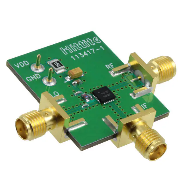
Evaluation PCB
B
SO
Recommended Components Values (IF = DC - 300 MHz)
C3
1000 pF
C4
2.2 µF
C1, C2, C5
100 pF
L1
18 nH
R1
18 Ohm
Mixers - High IP3 - SMT
TE
Application Circuit
Note :
O
Select R1 to achieve Icc by using equation below,
R1 ≥ 18 Ohms.
Icc = ( Vs - 3.8 ) / R1
List of Materials for Evaluation PCB 115906 [1]
Item
Description
J1 - J3
PCB Mount SMA RF Connector
J4, J5
DC Pin
C1, C2, C5
100 pF Chip Capacitor, 0402 Pkg.
C3
1000 pF Chip Capacitor, 0603 Pkg.
C4
2.2 µF Capacitor, Tantalum
L1
18 nH Chip Inductor, 0603 Pkg.
R1
18 Ohm Resistor, 1210 1/8 watt Pkg.
U1
HMC615LP4E
PCB [2]
113417 Evaluation Board
The circuit board used in the application should use
RF circuit design techniques. Signal lines should
have 50 Ohm impedance while the package ground
leads and exposed paddle should be connected
directly to the ground plane similar to that shown.
A sufficient number of via holes should be used to
connect the top and bottom ground planes. The
evaluation circuit board shown is available from Hittite upon request.
[1] Reference this number when ordering complete evaluation PCB
[2] Circuit Board Material: Rogers 4350
Information furnished by Analog Devices is believed to be accurate and reliable. However, no
For price,2 delivery,
andDrive,
to placeChelmsford,
orders: AnalogMA
Devices,
For price, delivery and to place orders: Hittite Microwave Corporation,
Elizabeth
01824Inc.,
responsibility is assumed by Analog Devices for its use, nor for any infringements of patents or other
One Technology Way, P.O. Box 9106, Norwood, MA 02062-9106
rights of third parties that may
result
from
its
use.
Specifications
subject
to
change
without
notice.
No
Phone: 978-250-3343
Fax: 978-250-3373
Order
at www.hittite.com
Phone: On-line
781-329-4700
• Order online at www.analog.com
license is granted by implication or otherwise under any patent or patent rights of Analog Devices.
Application
Support: Phone: 1-800-ANALOG-D
Trademarks and registered trademarks are
the property of their
respective owners.
Application
Support:
Phone: 978-250-3343
or apps@hittite.com
6
�