HMC580ST89 / 580ST89E
v04.0710
Features
The HMC580ST89 / HMC580ST89E is ideal forr:
P1dB Output Power: +22 dBm
• Cellular / PCS / 3G
Gain: 22 dB
• Fixed Wireless & WLAN
Output IP3: +37 dBm
• CATV, Cable Modem & DBS
Cascadable 50 Ohm I/Os
• Microwave Radio & Test Equipment
Single Supply: +5V
• IF & RF Applications
Industry Standard SOT89 Package
Functional Diagram
General Description
TE
Typical Applications
B
SO
LE
The HMC580ST89 & HMC580ST89E are InGaP
Heterojunction Bipolar Transistor (HBT) Gain
Block MMIC SMT amplifiers covering DC to 1 GHz.
Packaged in an industry standard SOT89, the
amplifier can be used as a cascadable 50 Ohm RF
or IF gain stage as well as a PA or LO driver with
up to +26 dBm output power. The HMC580ST89(E)
offers 22 dB of gain with a +37 dBm output IP3 at 250
MHz, and can operate directly from a +5V supply. The
HMC580ST89(E) exhibits excellent gain and output
power stability over temperature, while requiring a
minimal number of external bias components.
Electrical Specifi cations, Vs= 5V, Rbias= 1.8 Ohm, TA = +25° C
Parameter
O
AMPLIFIERS - DRIVER & GAIN BLOCK - SMT
8
InGaP HBT GAIN BLOCK
MMIC AMPLIFIER, DC - 1 GHz
Gain
Gain Variation Over Temperature
Input Return Loss
Output Return Loss
Reverse Isolation
Output Power for 1 dB Compression (P1dB)
Output Third Order Intercept (IP3)
(Pout= 0 dBm per tone, 1 MHz spacing)
Noise Figure
Supply Current (Icq)
DC - 0.25 GHz
0.25 - 0.50 GHz
0.50 - 1.00 GHz
DC - 1.0 GHz
DC - 0.25 GHz
0.25 - 0.50 GHz
0.50 - 1.00 GHz
DC - 0.50 GHz
0.50 - 1.00 GHz
DC - 1.0 GHz
DC - 0.25 GHz
0.25 - 0.50 GHz
0.50 - 1.00 GHz
DC - 0.25 GHz
0.25 - 0.50 GHz
0.50 - 1.00 GHz
DC - 1.0 GHz
Min.
Typ.
19
18.5
15
22
21
17
0.005
35
28
19
12
11
23
22
20.5
19
37
35
33
2.8
19
17.5
16
88
Max.
Units
dB
dB
dB
dB/ °C
dB
dB
dB
dB
dB
dB
dBm
dBm
dBm
dBm
dBm
dBm
dB
110
mA
Note: Data taken with broadband bias tee on device output.
8 - 146
For price, delivery and to place orders: Hittite Microwave Corporation, 20 Alpha Road, Chelmsford, MA 01824
Phone: 978-250-3343
Fax: 978-250-3373
Order On-line at www.hittite.com
Application Support: Phone: 978-250-3343 or apps@hittite.com
�HMC580ST89 / 580ST89E
v04.0710
InGaP HBT GAIN BLOCK
MMIC AMPLIFIER, DC - 1 GHz
Gain vs. Temperature
GAIN (dB)
S21
S11
S22
16
12
+25C
+85C
-40C
TE
8
4
0
0.5
1
1.5
2
2.5
0
3
FREQUENCY (GHz)
0.25
0.75
1
1.25
1.5
0
LE
FREQUENCY (GHz)
Input Return Loss vs. Temperature
Output Return Loss vs. Temperature
0
-5
+25C
+85C
-40C
-10
-5
-20
-25
-30
-40
-45
0
B
SO
-15
-35
0.3
0.5
0.8
1
1.3
-10
-15
+25C
+85C
-40C
-20
-25
1.5
0
0.25
FREQUENCY (GHz)
O
Reverse Isolation vs. Temperature
0.5
0.75
1
1.25
1.5
1.25
1.5
FREQUENCY (GHz)
Noise Figure vs. Temperature
10
0
-5
-10
-15
8
NOISE FIGURE (dB)
REVERSE ISOLATION (dB)
0.5
AMPLIFIERS - DRIVER & GAIN BLOCK - SMT
20
0
RETURN LOSS (dB)
8
24
25
20
15
10
5
0
-5
-10
-15
-20
-25
-30
-35
-40
RETURN LOSS (dB)
RESPONSE (dB)
Broadband Gain & Return Loss
+25C
+85C
-40C
-20
-25
+25C
+85C
-40C
6
4
2
-30
0
-35
0
0.25
0.5
0.75
1
FREQUENCY (GHz)
1.25
1.5
0
0.25
0.5
0.75
1
FREQUENCY (GHz)
For price, delivery and to place orders: Hittite Microwave Corporation, 20 Alpha Road, Chelmsford, MA 01824
Phone: 978-250-3343
Fax: 978-250-3373
Order On-line at www.hittite.com
Application Support: Phone: 978-250-3343 or apps@hittite.com
8 - 147
�HMC580ST89 / 580ST89E
v04.0710
InGaP HBT GAIN BLOCK
MMIC AMPLIFIER, DC - 1 GHz
P1dB vs. Temperature
24
Psat (dBm)
20
+25C
+85C
-40C
12
8
4
0
0.3
0.5
0.8
1
1.3
0
1.5
FREQUENCY (GHz)
+25C
+85C
-40C
25
20
0
0.25
0.5
0.75
1
0.75
1.25
1.5
Vcc vs. Icc Over Temperature for
Fixed Vs= 5V, RBIAS= 1.8 Ohms
32
28
24
20
16
Gain
P1dB
Psat
IP3
12
8
4
0
4.5
5
5.5
ACPR vs. Channel Output Power
O
-20
+85C
-25
WCDMA 140MHz
WCDMA 400MHz
CDMA2000 140MHz
CDMA2000 400MHz
-30
+25C
ACPR (dBc)
Icc (mA)
1.5
Vs (V)
94
88
86
84
-35
-40
-45
-50
82
-55
-40C
80
78
4.82
1.25
36
FREQUENCY (GHz)
92
1
LE
B
SO
40
30
0.5
Gain, Power & OIP3 vs. Supply Voltage
for Constant Icc = 88 mA @ 850 MHz
45
35
0.25
FREQUENCY (GHz)
Output IP3 vs. Temperature
90
-60
-65
4.83
4.84
4.85
Vcc (V)
8 - 148
16
TE
+25C
+85C
-40C
GAIN (dB), P1dB (dBm), Psat (dBm), IP3 (dBm)
P1dB (dBm)
28
26
24
22
20
18
16
14
12
10
8
6
4
2
0
0
IP3 (dBm)
AMPLIFIERS - DRIVER & GAIN BLOCK - SMT
8
Psat vs. Temperature
4.86
4.87
2
4
6
8
10
12
14
16
18
CHANNEL OUTPUT POWER (dBm)
For price, delivery and to place orders: Hittite Microwave Corporation, 20 Alpha Road, Chelmsford, MA 01824
Phone: 978-250-3343
Fax: 978-250-3373
Order On-line at www.hittite.com
Application Support: Phone: 978-250-3343 or apps@hittite.com
�HMC580ST89 / 580ST89E
v04.0710
InGaP HBT GAIN BLOCK
MMIC AMPLIFIER, DC - 1 GHz
Absolute Maximum Ratings
+5.5 Vdc
RF Input Power (RFIN)(Vcc = +4.2 Vdc)
+10 dBm
Junction Temperature
150 °C
Continuous Pdiss (T = 85 °C)
(derate 9 mW/°C above 85 °C)
0.59 W
Thermal Resistance
(junction to lead)
110 °C/W
Storage Temperature
-65 to +150 °C
Operating Temperature
-40 to +85 °C
ESD Sensitivity (HMB)
Class 1C
TE
B
SO
LE
Outline Drawing
ELECTROSTATIC SENSITIVE DEVICE
OBSERVE HANDLING PRECAUTIONS
NOTES:
1. PACKAGE BODY MATERIAL:
MOLDING COMPOUND MP-180S OR EQUIVALENT.
2. LEAD MATERIAL: Cu w/ Ag SPOT PLATING.
3. LEAD PLATING: 100% MATTE TIN.
O
4. DIMENSIONS ARE IN INCHES [MILLIMETERS]
5. DIMENSION DOES NOT INCLUDE MOLDFLASH OF 0.15mm PER SIDE.
6. DIMENSION DOES NOT INCLUDE MOLDFLASH OF 0.25mm PER SIDE.
8
AMPLIFIERS - DRIVER & GAIN BLOCK - SMT
Collector Bias Voltage (Vcc)
7. ALL GROUND LEADS MUST BE SOLDERED TO PCB RF GROUND.
Package Information
Part Number
Package Body Material
Lead Finish
MSL Rating
HMC580ST89
Low Stress Injection Molded Plastic
Sn/Pb Solder
MSL1
HMC580ST89E
RoHS-compliant Low Stress Injection Molded Plastic
100% matte Sn
MSL1
Package Marking [3]
[1]
H580
XXXX
[2]
H580
XXXX
[1] Max peak reflow temperature of 235 °C
[2] Max peak reflow temperature of 260 °C
[3] 4-Digit lot number XXXX
For price, delivery and to place orders: Hittite Microwave Corporation, 20 Alpha Road, Chelmsford, MA 01824
Phone: 978-250-3343
Fax: 978-250-3373
Order On-line at www.hittite.com
Application Support: Phone: 978-250-3343 or apps@hittite.com
8 - 149
�HMC580ST89 / 580ST89E
v04.0710
InGaP HBT GAIN BLOCK
MMIC AMPLIFIER, DC - 1 GHz
Pin Descriptions
Function
Description
Interface Schematic
1
IN
This pin is DC coupled.
An off chip DC blocking capacitor is required.
3
OUT
RF output and DC Bias (Vcc) for the output stage.
2, 4
GND
These pins and package bottom
must be connected to RF/DC ground.
LE
TE
Pin Number
B
SO
Application Circuit
O
AMPLIFIERS - DRIVER & GAIN BLOCK - SMT
8
Recommended Bias Resistor Values
for Icc = 88 mA, Rbias = (Vs - Vcc) / Icc, Vs > +5V
6V
8V
RBIAS VALUE
Supply Voltage (Vs)
13 Ω
36 Ω
RBIAS POWER RATING
¼W
½W
Note:
1. External blocking capacitors are required on
RFIN and RFOUT.
2. RBIAS provides DC bias stability over temperature.
Recommended Component Values for Key Application Frequencies with Vs = +5V
Frequency (MHz)
Component
L1
8 - 150
50
250
400
900
270 nH
110 nH
110 nH
56 nH
C1, C2
0.01 μF
820 pF
820 pF
100 pF
Rbias
0 Ohms
1.5 Ohms
1.5 Ohms
1.8 Ohms
For price, delivery and to place orders: Hittite Microwave Corporation, 20 Alpha Road, Chelmsford, MA 01824
Phone: 978-250-3343
Fax: 978-250-3373
Order On-line at www.hittite.com
Application Support: Phone: 978-250-3343 or apps@hittite.com
�HMC580ST89 / 580ST89E
v04.0710
InGaP HBT GAIN BLOCK
MMIC AMPLIFIER, DC - 1 GHz
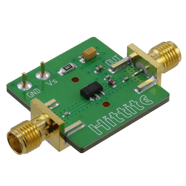
Evaluation PCB
O
List of Materials for Evaluation PCB 116402 [1]
Item
Description
J1 - J2
PCB Mount SMA Connector
J3 - J4
DC Pin
C1, C2
Capacitor, 0402 Pkg.
C3
100 pF Capacitor, 0402 Pkg.
C4
1000 pF Capacitor, 0603 Pkg.
C5
2.2 μF Capacitor, Tantalum
R1
Resistor, 1206 Pkg.
L1
Inductor, 0603 Pkg.
U1
HMC580ST89 / HMC580ST89E
PCB [2]
107368 Evaluation PCB
The circuit board used in the final application
should use RF circuit design techniques. Signal
lines should have 50 Ohm impedance while the
package ground leads and package bottom should
be connected directly to the ground plane similar to
that shown. A sufficient number of via holes should
be used to connect the top and bottom ground
planes. The evaluation board should be mounted
to an appropriate heat sink. The evaluation circuit
board shown is available from Hittite upon request.
AMPLIFIERS - DRIVER & GAIN BLOCK - SMT
B
SO
LE
TE
8
[1] Reference this number when ordering complete evaluation PCB
[2] Circuit Board Material: Rogers 4350
[3] Evaluation board tuned for 900 MHz operation
For price, delivery and to place orders: Hittite Microwave Corporation, 20 Alpha Road, Chelmsford, MA 01824
Phone: 978-250-3343
Fax: 978-250-3373
Order On-line at www.hittite.com
Application Support: Phone: 978-250-3343 or apps@hittite.com
8 - 151
�