GaAs, InGaP, HBT, MMIC, Ultralow Phase Noise,
Distributed Amplifier, 2 GHz to 18 GHz
HMC606LC5
Data Sheet
Radars, electronic warfare (EW), and electronic counter
measures (ECMs)
Microwave radios
Test instrumentation
Military and space
Fiber optic systems
32
31
30
29
28
27
26
25
NC
VCC1
NC
GND
RFIN
GND
NC
NC
1
2
3
4
5
6
7
8
HMC606LC5
24
23
22
21
20
19
18
17
NC
NC
GND
RFOUT
GND
NC
NC
NC
PACKAGE
BASE
GND
14968-001
APPLICATIONS
NC
NC
NC
NC
NC
NC
NC
NC
FUNCTIONAL BLOCK DIAGRAM
Ultralow phase noise: −160 dBc/Hz typical at 10 kHz
Output power for 1 dB compression (P1dB): 15 dBm typical
at 2 GHz to 12 GHz frequency range
Gain: 13.5 dB typical at 2 GHz to 12 GHz frequency range
Output third-order intercept (IP3): 27 dBm typical at 2 GHz
to 12 GHz frequency range
Supply voltage: 5.0 V at 64 mA typical
50 Ω matched input/output
32-terminal, ceramic, leadless chip carrier (LCC)
NC 9
NC 10
NC 11
NC 12
NC 13
NC 14
NC 15
VCC2 16
FEATURES
Figure 1.
GENERAL DESCRIPTION
The HMC606LC5 is a gallium arsenide (GaAs), indium gallium
phosphide (InGaP), heterojunction bipolar transistor (HBT),
monolithic microwave integrated circuit (MMIC) distributed
amplifier housed in a 32-terminal, ceramic, leadless chip carrier
(LCC) package that operates from 2 GHz to 18 GHz. With an
input signal of 12 GHz, the amplifier provides ultralow phase noise
performance of −160 dBc/Hz at a 10 kHz offset, representing a
significant improvement over field effect transistor (FET)based distributed amplifiers.
Rev. J
The HMC606LC5 provides 13.5 dB of small signal gain, 27 dBm
output IP3, and 15 dBm of output power for 1 dB compression
while requiring 64 mA from a 5.0 V supply. The input and output
of the HMC606LC5 amplifier are internally matched to 50 Ω
and are internally dc blocked.
Document Feedback
Information furnished by Analog Devices is believed to be accurate and reliable. However, no
responsibility is assumed by Analog Devices for its use, nor for any infringements of patents or other
rights of third parties that may result from its use. Specifications subject to change without notice.
No license is granted by implication or otherwise under any patent or patent rights of Analog
Devices. Trademarks and registered trademarks are the property of their respective owners.
One Technology Way, P.O. Box 9106, Norwood, MA 02062-9106, U.S.A.
Tel: 781.329.4700 ©2017–2020 Analog Devices, Inc. All rights reserved.
Technical Support
www.analog.com
�HMC606LC5
Data Sheet
TABLE OF CONTENTS
Features .............................................................................................. 1
Pin Configuration and Function Descriptions .............................5
Applications ...................................................................................... 1
Interface Schematics .....................................................................5
Functional Block Diagram .............................................................. 1
Typical Performance Characteristics .............................................6
General Description ......................................................................... 1
Applications Information ................................................................8
Revision History ............................................................................... 2
Evaluation Printed Circuit Board (PCB) ...................................8
Specifications .................................................................................... 3
Outline Dimensions ..........................................................................9
Electrical Specifications ............................................................... 3
Ordering Guide .............................................................................9
Absolute Maximum Ratings ........................................................... 4
ESD Caution.................................................................................. 4
REVISION HISTORY
3/2020—Rev. I to Rev. J
Deleted Figure 16, Figure 17, and Figure 18; Renumbered
Sequentially ....................................................................................... 8
1/2018—Rev. H to Rev. I
Changes to Figure 16, Figure 16 Caption, Figure 17, Figure 17
Caption, Figure 18, Figure 18 Caption, and Figure 19 ................ 8
Changes to Ordering Guide .......................................................... 10
10/2017—Rev. G to Rev. H
Changes to Typical Performance Characteristics Section .......... 7
Added Figure 19; Renumbered Sequentially ................................ 9
Updated Outline Dimensions ...................................................... 10
Changes to Ordering Guide .......................................................... 10
8/2017—Rev. F to Rev. G
Changes to Continuous Power Dissipation, PDISS Parameter,
Table 4 .................................................................................................4
This Hittite Microwave Products data sheet has been reformatted
to meet the styles and standards of Analog Devices, Inc.
2/2017—Rev. 05.0514 to Rev. F
Updated Format .................................................................Universal
Changes to Features Section and General Description Section ....... 1
Changes to Table 4 ............................................................................4
Updated Outline Dimensions .........................................................9
Changes to Ordering Guide .............................................................9
Rev. J | Page 2 of 9
�Data Sheet
HMC606LC5
SPECIFICATIONS
ELECTRICAL SPECIFICATIONS
TA = 25°C, VCC1 = VCC2 = 5 V, unless otherwise noted.
Table 1.
Parameter
FREQUENCY RANGE
GAIN
Flatness
Variation Over Temperature
NOISE FIGURE
INPUT RETURN LOSS
OUTPUT
Return Loss
Power for 1 dB Compression (P1dB)
Saturated Power (PSAT)
Third-Order Intercept (IP3)
PHASE NOISE
At 100 Hz
At 1 kHz
At 10 kHz
At 1 MHz
SUPPLY CURRENT
Min
2
10.5
12
Typ
Max
12
13.5
±1.0
0.021
5
20
Unit
GHz
dB
dB
dB/°C
dB
dB
15
15
17
27
dB
dBm
dBm
dBm
−140
−150
−160
−170
64
dBc/Hz
dBc/Hz
dBc/Hz
dBc/Hz
mA
95
Table 2.
Parameter
FREQUENCY RANGE
GAIN
Flatness
Variation Over Temperature
NOISE FIGURE
INPUT RETURN LOSS
OUTPUT
Return Loss
Power for 1 dB Compression (P1dB)
Saturated Power (PSAT)
Third-Order Intercept (IP3)
PHASE NOISE
At 100 Hz
At 1 kHz
At 10 kHz
At 1 MHz
SUPPLY CURRENT
Min
2
9.5
10
Table 3. VCC1, VCC2 vs. Typical Supply Current
VCC1, VCC2 (V)
4.5
5.0
5.5
ICC1 + ICC2 (mA)
53
64
71
Rev. J | Page 3 of 9
Typ
Max
18
12.5
±1.0
0.024
7
18
Unit
GHz
dB
dB
dB/°C
dB
dB
15
13
15
22
dB
dBm
dBm
dBm
−140
−150
−160
−170
64
dBc/Hz
dBc/Hz
dBc/Hz
dBc/Hz
mA
95
�HMC606LC5
Data Sheet
ABSOLUTE MAXIMUM RATINGS
Stresses at or above those listed under Absolute Maximum
Ratings may cause permanent damage to the product. This is a
stress rating only; functional operation of the product at these
or any other conditions above those indicated in the
operational section of this specification is not implied.
Operation beyond the maximum operating conditions for
extended periods may affect product reliability.
Table 4.
Parameter
VCC1 = VCC2
RF Input Power (RFIN)
Channel Temperature
Continuous Power Dissipation, PDISS (TA =
85°C, Derate 10.9 mW/°C Above 85°C)
Maximum Peak Reflow Temperature (MSL3)1
Thermal Resistance (Channel to Ground
Paddle)
Storage Temperature Range
Operating Temperature Range
ESD Sensitivity (Human Body Model, HBM)
1
Rating
7V
15 dBm
175°C
0.978 W
ESD CAUTION
260°C
92°C/W
−65°C to +150°C
−40°C to +85°C
Class 0, Pass 100 V
See the Ordering Guide section.
Rev. J | Page 4 of 9
�Data Sheet
HMC606LC5
32
31
30
29
28
27
26
25
NC
NC
NC
NC
NC
NC
NC
NC
PIN CONFIGURATION AND FUNCTION DESCRIPTIONS
HMC606LC5
TOP VIEW
(Not to Scale)
24
23
22
21
20
19
18
17
NC
NC
GND
RFOUT
GND
NC
NC
NC
PACKAGE
BASE
GND
NOTES
1. NC = NO CONNECT. THESE PINS MAY BE CONNECTED TO RF
GROUND. PERFORMANCE WILL NOT BE AFFECTED.
2. THE EXPOSED PAD MUST BE CONNECTED TO RF/DC GROUND.
14968-020
1
2
3
4
5
6
7
8
NC 9
NC 10
NC 11
NC 12
NC 13
NC 14
NC 15
VCC2 16
NC
VCC1
NC
GND
RFIN
GND
NC
NC
Figure 2. Pin Configuration
Table 5. Pin Function Descriptions
Pin No.
1, 3, 7 to 15, 17 to 19, 23 to 32
2, 16
4, 6, 20, 22
Mnemonic
NC
VCC1, VCC2
GND
5
RFIN
21
RFOUT
EPAD
Description
No Connect. These pins may be connected to RF ground. Performance will not be affected.
Power Supply Voltages for the Amplifier. See Figure 3 for the interface schematic.
Ground. These pins must be connected to RF/dc ground. See Figure 4 for the interface
schematic.
RF Input. This pin is ac-coupled and matched to 50 Ω. See Figure 5 for the interface
schematic.
RF Output. This pin is ac-coupled and matched to 50 Ω. See Figure 6 for the interface
schematic.
Exposed Pad. The exposed pad must be connected to RF/dc ground.
14968-004
INTERFACE SCHEMATICS
VCC1, VCC2
14968-002
RFIN
Figure 3. VCC1, VCC2 Interface Schematic
RFOUT
14968-005
14968-003
GND
Figure 5. RFIN Interface Schematic
Figure 6. RFOUT Interface Schematic
Figure 4. GND Interface Schematic
Rev. J | Page 5 of 9
�HMC606LC5
Data Sheet
TYPICAL PERFORMANCE CHARACTERISTICS
20
S11
S21
S22
+85°C
+25°C
–40°C
10
16
0
12
GAIN (dB)
–10
8
0
2
4
6
8
10
12
14
16
18
20
22
FREQUENCY (GHz)
0
14968-006
–30
2
4
6
8
10
12
14
Figure 7. Response (Gain and Return Loss) vs. Frequency
0
+85°C
+25°C
–40°C
+85°C
+25°C
–40°C
–5
OUTPUT RETURN LOSS (dB)
–5
–10
–15
–20
–25
–10
–15
–20
–25
2
4
6
8
10
12
14
16
18
FREQUENCY (GHz)
–30
14968-007
–30
2
4
6
8
10
12
14
16
18
FREQUENCY (GHz)
Figure 8. Input Return Loss vs. Frequency for Various Temperatures
14968-010
INPUT RETURN LOSS (dB)
18
Figure 10. Gain vs. Frequency for Various Temperatures
0
Figure 11. Output Return Loss vs. Frequency for Various Temperatures
20
14
+85°C
+25°C
–40°C
12
15
NOISE FIGURE (dB)
POUT (dBm), GAIN (dB). PAE (%)
16
FREQUENCY (GHz)
14968-009
4
–20
10
5
10
8
6
4
0
2
OUTPUT POWER
GAIN
PAE
–10
–5
0
PIN (dBm)
5
10
0
14968-008
–5
–15
2
4
6
8
10
12
14
16
18
FREQUENCY (GHz)
Figure 9. Output Power (POUT), Gain, and Power Added Efficiency (PAE) vs.
Input Power (PIN)
Rev. J | Page 6 of 9
Figure 12. Noise Figure vs. Frequency for Various Temperatures
14968-011
RESPONSE (dB)
20
�Data Sheet
HMC606LC5
20
25
+85°C
+25°C
–40°C
+85°C
+25°C
–40°C
21
PSAT (dBm)
12
8
4
13
9
2
4
6
8
10
12
14
16
18
FREQUENCY (GHz)
5
14968-012
0
2
4
6
8
10
12
14
16
18
FREQUENCY (GHz)
Figure 13. Power for 1 dB Compression (P1dB) vs. Frequency for Various
Temperatures
Figure 15. Saturated Power (PSAT) vs. Frequency for Various Temperatures
35
–80
+85°C
+25°C
–40°C
–90
ADDITIVE PHASE NOISE (dBc/Hz)
30
OUTPUT IP3 (dBm)
17
14968-015
P1dB (dBm)
16
25
20
15
10
–100
–110
–120
–130
–140
–150
–160
4
6
8
10
12
FREQUENCY (GHz)
14
16
18
–180
100
14968-013
2
1k
10k
100k
OFFSET FREQUENCY (Hz)
Figure 14. Output Third-Order Intercept (IP3) vs. Frequency for Various
Temperatures
Figure 16. Additive Phase Noise vs. Offset Frequency,
RF Frequency = 8 GHz, RF Input Power = 12 dBm (PSAT)
Rev. J | Page 7 of 9
1M
14968-021
–170
5
�HMC606LC5
Data Sheet
APPLICATIONS INFORMATION
EVALUATION PRINTED CIRCUIT BOARD (PCB)
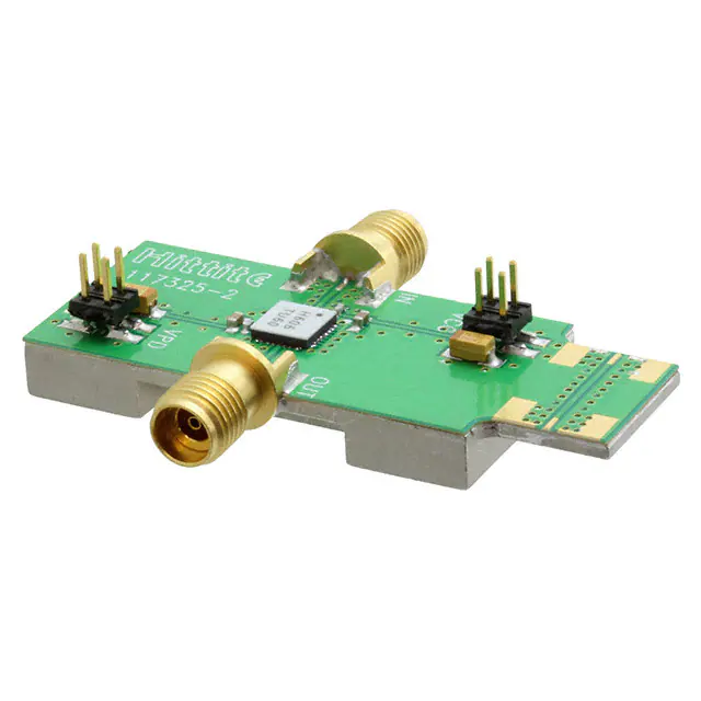
14968-018
The circuit board used in the application must use RF circuit
design techniques. Signal lines must have 50 Ω impedance, and
the package ground leads and package bottom must be connected
directly to the ground plane similar to that shown in Figure 17.
Use a sufficient number of via holes to connect the top and bottom
ground planes. Mount the evaluation PCB to an appropriate
heat sink. The evaluation PCB shown in Figure 17 is available
from Analog Devices, Inc., upon request.
Figure 17. Evaluation PCB
Table 6. List of Materials for Evaluation PCB (117156-HMC606LC51)
Item
J1, J2
J3, J4
C1, C2
C3, C4
C5, C6
U1
PCB
1
Description
SRI K connectors
2 mm Molex headers
4.7 μF, tantalum capacitors
100 pF capacitors, 0402 package
1000 pF capacitors, 0603 package
HMC606LC5
117325-1 evaluation PCB; circuit board material: Rogers 4350
Reference this number when ordering the complete evaluation PCB.
Rev. J | Page 8 of 9
�Data Sheet
HMC606LC5
OUTLINE DIMENSIONS
5.05
4.90 SQ
4.75
PIN 1
INDICATOR
0.36
0.30
0.24
0.08
REF
1
0.50
BSC
3.60
3.50 SQ
3.40
EXPOSED
PAD
17
0.38
0.32
0.26
TOP VIEW
1.10
1.00
0.90
PIN 1
32
25
24
8
16
9
BOTTOM VIEW
0.20 MIN
3.50 REF
4.10 REF
FOR PROPER CONNECTION OF
THE EXPOSED PAD, REFER TO
THE PIN CONFIGURATION AND
FUNCTION DESCRIPTIONS
SECTION OF THIS DATA SHEET.
PKG-004843
SEATING
PLANE
04-24-2017-D
SIDE VIEW
Figure 18. 32-Terminal Ceramic Leadless Chip Carrier [LCC]
(E-32-1)
Dimensions shown in millimeters
ORDERING GUIDE
Model 1
HMC606LC5
HMC606LC5TR
HMC606LC5TR-R5
117156-HMC606LC5
1
2
Temperature Range
−40°C to +85°C
−40°C to +85°C
−40°C to +85°C
MSL Rating 2
MSL3
MSL3
MSL3
Package Description
32-Terminal Ceramic Leadless Chip Carrier [LCC]
32-Terminal Ceramic Leadless Chip Carrier [LCC]
32-Terminal Ceramic Leadless Chip Carrier [LCC]
Evaluation Board
All models are RoHS Compliant.
See the Absolute Maximum Ratings section.
©2017–2020 Analog Devices, Inc. All rights reserved. Trademarks and
registered trademarks are the property of their respective owners.
D14968-3/20(J)
Rev. J | Page 9 of 9
Package Option
E-32-1
E-32-1
E-32-1
�