HMC631LP3 / 631LP3E
v00.1007
GaAs HBT VECTOR
MODULATOR 1.8 - 2.7 GHz
Typical Applications
Features
The HMC631LP3(E) is ideal for:
Continuous Phase Control: 360°
• Cellular/3G & WiMAX Systems
Continuous Gain Control: 40 dB
• Wireless Infrastructure HPA &
MCPA Error Correction
Output Noise Floor: -160 dBm/Hz
Input IP3: +35 dBm
• Pre-Distortion or Feed-Forward Linearization
16 Lead 3x3mm SMT Package: 9mm2
• Beam Forming & Nulling Circuits
MODULATORS - SMT
10
General Description
Functional Diagram
The HMC631LP3 & HMC631LP3E are high dynamic
range Vector Modulator RFICs which are targeted
for RF predistortion and feed-forward cancellation
circuits, as well as RF cancellation, beam forming and
amplitude/phase correction circuits. The I & Q ports
of the HMC631LP3(E) can be used to continuously
vary the phase and amplitude of RF signals by up to
360 degrees and 40 dB respectively, while supporting
a 3 dB modulation bandwidth of 200 MHz. With an
output IP3 of +26 dBm and output noise floor of -160
dBm/Hz (at maximum gain setting), the IP3/noise floor
ratio is 186 dB.
Electrical Specifi cations, TA = +25° C, Vcc= +8V
Parameter
Min.
Frequency Range
Typ.
Max.
Min.
Typ.
Max.
Units
1.8 - 2.2
2.2 - 2.7
-9
-11
dB
0.016
dB / °C
0.15
0.4
dB
Gain Range
40
40
dB
Input Return Loss
9
9
dB
Maximum Gain[1]
-11
Gain Variation Over Temperature
0.016
Gain Flatness Across Any 60 MHz Bandwidth
Output Return Loss
Input Power for 1dB Compression (P1dB)
Input Third Order Intercept (IP3)
Output Noise
Control Port Bandwidth (-3 dB)
Control Port Impedance
Control Port Capacitance
Control Voltage Range
15
0.025
GHz
13
10
dB
18
21
dBm
35
37
dBm
-160
-160
dBm/Hz
200
200
MHz
1.45k
1.45k
Ohms
0.22
0.22
pF
+0.5 to +2.5
+0.5 to +2.5
Vdc
Group Delay Variation Over 60 MHz Bandwidth
20
20
ps
Supply Current (Icq)
93
93
mA
Unless otherwise noted, measurements are made @ max. gain setting and 45˚ phase setting. See application circuit for details.
[1]
Includes loss of input balun (0.8 dB typ.)
10 - 58
For price, delivery, and to place orders, please contact
Hittite
Microwave
Corporation:
For price,
delivery,
and to place
orders: Analog Devices, Inc.,
One Technology Way,
P.O. 978-250-3373
Box 9106, Norwood, MA 02062-9106
20 Alpha Road, Chelmsford, MA 01824 Phone: 978-250-3343
Fax:
Phone: 781-329-4700 • Order online at www.analog.com
Order On-line at www.hittite.com
Application Support: Phone: 1-800-ANALOG-D
Information furnished by Analog Devices is believed to be accurate and reliable. However, no
responsibility is assumed by Analog Devices for its use, nor for any infringements of patents or other
rights of third parties that may result from its use. Specifications subject to change without notice. No
license is granted by implication or otherwise under any patent or patent rights of Analog Devices.
Trademarks and registered trademarks are the property of their respective owners.
�HMC631LP3 / 631LP3E
v00.1007
GaAs HBT VECTOR
MODULATOR 1.8 - 2.7 MHz
Maximum Gain vs. Supply Voltage
0
0
-2
-2
-4
-4
-6
-6
GAIN (dB)
-8
-10
-12
-14
-12
-14
+25C
+85C
-40C
-16
-8
-10
7.6V
8.0V
8.4V
-16
-18
-18
-20
1.7
1.8
1.9
2
2.1
2.2
2.3
2.4
2.5
2.6
2.7
-20
1.7
2.8
1.8
1.9
2
FREQUENCY (GHz)
2.1
2.2
2.3
2.4
2.5
2.6
2.7
2.8
FREQUENCY (GHz)
Phase vs. Phase Settings @ F= 2 GHz
vs. Various Gain Settings
Gain vs. Phase Settings @ F= 2 GHz
0
360
315
PHASE (DEGREES)
GAIN (dB)
-10
-20
-30
MAX
-5 dB
-40
-10 dB
-20 dB
270
MAX
-5 dB
-10 dB
-20 dB
225
180
135
90
45
0
-50
0
45
90
135
180
225
270
315
360
0
45
90
180
225
270
315
360
Output Return Loss vs. Temperature
0
0
-5
-5
RETURN LOSS (dB)
RETURN LOSS (dB)
Input Return Loss vs. Temperature
-10
+25C
+85C
-40C
-20
-25
1.7
135
PHASE SETTING (DEGREES)
PHASE SETTING (DEGREES)
-15
10
MODULATORS - SMT
GAIN (dB)
Maximum Gain vs. Temperature
+25C
+85C
-40C
-10
-15
-20
1.8
1.9
2
2.1
2.2
2.3
2.4
2.5
2.6
2.7
2.8
FREQUENCY (GHz)
-25
1.7
1.8
1.9
2
2.1
2.2
2.3
2.4
2.5
2.6
2.7
2.8
FREQUENCY (GHz)
For price, delivery, and to place orders, please contact
Hittite
Microwave
Corporation:
For price,
delivery,
and to place
orders: Analog Devices, Inc.,
One Technology Way,
P.O. 978-250-3373
Box 9106, Norwood, MA 02062-9106
20 Alpha Road, Chelmsford, MA 01824 Phone: 978-250-3343
Fax:
Phone: 781-329-4700 • Order online at www.analog.com
Order On-line at www.hittite.com
Application Support: Phone: 1-800-ANALOG-D
Information furnished by Analog Devices is believed to be accurate and reliable. However, no
responsibility is assumed by Analog Devices for its use, nor for any infringements of patents or other
rights of third parties that may result from its use. Specifications subject to change without notice. No
license is granted by implication or otherwise under any patent or patent rights of Analog Devices.
Trademarks and registered trademarks are the property of their respective owners.
10 - 59
�HMC631LP3 / 631LP3E
v00.1007
GaAs HBT VECTOR
MODULATOR 1.8 - 2.7 MHz
Output Noise vs.
Phase Settings @ F= 2 GHz
Output Noise vs. Temperature
-160
NOISE (dBm/Hz)
NOISE (dBm/Hz)
-162
-164
-166
+25C
+85C
-40C
-168
10
-170
1.7
1.8
1.9
2
2.1
2.2
2.3
2.4
2.5
2.6
2.7
-150
-152
-154
-156
-158
-160
-162
-164
-166
-168
-170
-172
-174
-176
-178
-180
2.8
0
45
90
135
180
225
315
360
Input IP3 vs. Temperature
22
44
42
20
IP3 (dBm)
40
18
+25C
+85C
-40C
16
38
36
34
32
+25C
+85C
-40C
14
30
12
1.7
1.8
1.9
2
2.1
2.2
2.3
2.4
2.5
2.6
2.7
28
1.8
2.8
1.9
Group Delay
2.1
2.2
2.4
90
1
750
120
60
0.8
0.6
MAGNITUDE G/Gmax
700
650
600
550
30
0.4
0.2
0
0
330
210
500
1.7
2.3
Linear Gain vs. Phase Setting
800
GROUP DELAY (ps)
2
FREQUENCY (GHz)
FREQUENCY (GHz)
1.8
1.9
2
2.1
2.2
2.3
2.4
2.5
2.6
2.7
2.8
FREQUENCY (GHz)
10 - 60
270
PHASE SETTING (DEGREES)
Input P1dB vs. Temperature
P1dB (dBm)
MODULATORS - SMT
FREQUENCY (GHz)
240
300
270
For price, delivery, and to place orders, please contact
Hittite
Microwave
Corporation:
For price,
delivery,
and to place
orders: Analog Devices, Inc.,
One Technology Way,
P.O. 978-250-3373
Box 9106, Norwood, MA 02062-9106
20 Alpha Road, Chelmsford, MA 01824 Phone: 978-250-3343
Fax:
Phone: 781-329-4700 • Order online at www.analog.com
Order On-line at www.hittite.com
Application Support: Phone: 1-800-ANALOG-D
Information furnished by Analog Devices is believed to be accurate and reliable. However, no
responsibility is assumed by Analog Devices for its use, nor for any infringements of patents or other
rights of third parties that may result from its use. Specifications subject to change without notice. No
license is granted by implication or otherwise under any patent or patent rights of Analog Devices.
Trademarks and registered trademarks are the property of their respective owners.
�HMC631LP3 / 631LP3E
v00.1007
GaAs HBT VECTOR
MODULATOR 1.8 - 2.7 MHz
Typical Supply Current vs. Vcc
Absolute Maximum Ratings
Vcc (V)
Icc (mA)
RF Input (Vcc = +8V)
27 dBm
7.6
88
Supply Voltage (Vcc)
+10V
8.0
93
I & Q Input
-0.5V to +5V
8.4
99
Junction Temperature (Tc)
135 °C
Continuous Pdiss (T = 85°C)
(Derate 34 mW/°C above 85°C)
1.7 W
Thermal Resistance (Rth)
(junction to ground paddle)
29.6 °C/W
Storage Temperature
-65 to +150 °C
Operating Temperature
-40 to +85 °C
Note:
Modulator will operate over full voltage range shown above.
10
MODULATORS - SMT
ELECTROSTATIC SENSITIVE DEVICE
OBSERVE HANDLING PRECAUTIONS
Outline Drawing
NOTES:
1. LEADFRAME MATERIAL: COPPER ALLOY
2. DIMENSIONS ARE IN INCHES [MILLIMETERS].
3. LEAD SPACING TOLERANCE IS NON-CUMULATIVE
4. PAD BURR LENGTH SHALL BE 0.15mm MAXIMUM.
PAD BURR HEIGHT SHALL BE 0.05mm MAXIMUM.
5. PACKAGE WARP SHALL NOT EXCEED 0.05mm.
6. ALL GROUND LEADS AND GROUND PADDLE MUST
BE SOLDERED TO PCB RF GROUND.
7. REFER TO HITTITE APPLICATION NOTE FOR SUGGESTED
PCB LAND PATTERN.
Package Information
Part Number
Package Body Material
Lead Finish
MSL Rating
HMC631LP3
Low Stress Injection Molded Plastic
Sn/Pb Solder
MSL1
HMC631LP3E
RoHS-compliant Low Stress Injection Molded Plastic
100% matte Sn
MSL1
Package Marking [3]
[1]
631
XXXX
[2]
631
XXXX
[1] Max peak reflow temperature of 235 °C
[2] Max peak reflow temperature of 260 °C
[3] 4-Digit lot number XXXX
For price, delivery, and to place orders, please contact
Hittite
Microwave
Corporation:
For price,
delivery,
and to place
orders: Analog Devices, Inc.,
One Technology Way,
P.O. 978-250-3373
Box 9106, Norwood, MA 02062-9106
20 Alpha Road, Chelmsford, MA 01824 Phone: 978-250-3343
Fax:
Phone: 781-329-4700 • Order online at www.analog.com
Order On-line at www.hittite.com
Application Support: Phone: 1-800-ANALOG-D
Information furnished by Analog Devices is believed to be accurate and reliable. However, no
responsibility is assumed by Analog Devices for its use, nor for any infringements of patents or other
rights of third parties that may result from its use. Specifications subject to change without notice. No
license is granted by implication or otherwise under any patent or patent rights of Analog Devices.
Trademarks and registered trademarks are the property of their respective owners.
10 - 61
�HMC631LP3 / 631LP3E
v00.1007
GaAs HBT VECTOR
MODULATOR 1.8 - 2.7 MHz
Pin Description
MODULATORS - SMT
10
10 - 62
Pin Number
Function
Description
1, 4, 10 - 12
N/C
No connection. These pins may be connected to RF ground.
Performance will not be affected
2, 3
IN, IN
Differential RF inputs, 100 Ohms differential impedance. (i.e.
each pin is 50 Ohms to ground). Must be DC blocked.
5, 15
I
In-phase control input. Pins 5 and 15 are redundant.
Either input can be used.
6, 16
Q
Quadrature control input. Pins 6 and 16 are redundant.
Either input can be used.
7, 8, 13, 14
Vcc
Supply Voltage, pins are DC connected on-chip. It is only necessary to supply Vcc to any 1 of the 4 pins, but all 4 pins must
be bypassed to ground. (See application circuit).
9
RFOUT
RF Output: Must be DC blocked.
GND
Ground: Backside of package has exposed metal ground
paddle which must be connected to RF/DC ground.
Interface Schematic
For price, delivery, and to place orders, please contact
Hittite
Microwave
Corporation:
For price,
delivery,
and to place
orders: Analog Devices, Inc.,
One Technology Way,
P.O. 978-250-3373
Box 9106, Norwood, MA 02062-9106
20 Alpha Road, Chelmsford, MA 01824 Phone: 978-250-3343
Fax:
Phone: 781-329-4700 • Order online at www.analog.com
Order On-line at www.hittite.com
Application Support: Phone: 1-800-ANALOG-D
Information furnished by Analog Devices is believed to be accurate and reliable. However, no
responsibility is assumed by Analog Devices for its use, nor for any infringements of patents or other
rights of third parties that may result from its use. Specifications subject to change without notice. No
license is granted by implication or otherwise under any patent or patent rights of Analog Devices.
Trademarks and registered trademarks are the property of their respective owners.
�HMC631LP3 / 631LP3E
v00.1007
GaAs HBT VECTOR
MODULATOR 1.8 - 2.7 MHz
Application Circuit
* Pins 15 & 16 are redundant I & Q inputs.
Gain and Phase control are applied through the I and Q control ports. For a given linear gain (G) and phase (θ) setting, the
voltages applied to these ports in all measurements are calculated as follows:
MODULATORS - SMT
10
G
Cos (θ )
G max
G
Q (G,θ ) = Vmq + 1.0V
Sin (θ )
G max
I (G,θ ) = Vmi + 1.0V
Where Vmi and Vmq are the I and Q voltage settings corresponding to maximum isolation at room temperature and F = 2 GHz.
Note that G=10X and Gmax = 10Y where x =
Gain Setting ( dB)
and
20
y = Max
Gain Setting( dB)
.
20
Nominally Vmi = Vmq = 1.5V, Gmax = 0.316.
For price, delivery, and to place orders, please contact
Hittite
Microwave
Corporation:
For price,
delivery,
and to place
orders: Analog Devices, Inc.,
One Technology Way,
P.O. 978-250-3373
Box 9106, Norwood, MA 02062-9106
20 Alpha Road, Chelmsford, MA 01824 Phone: 978-250-3343
Fax:
Phone: 781-329-4700 • Order online at www.analog.com
Order On-line at www.hittite.com
Application Support: Phone: 1-800-ANALOG-D
Information furnished by Analog Devices is believed to be accurate and reliable. However, no
responsibility is assumed by Analog Devices for its use, nor for any infringements of patents or other
rights of third parties that may result from its use. Specifications subject to change without notice. No
license is granted by implication or otherwise under any patent or patent rights of Analog Devices.
Trademarks and registered trademarks are the property of their respective owners.
10 - 63
�HMC631LP3 / 631LP3E
v00.1007
GaAs HBT VECTOR
MODULATOR 1.8 - 2.7 MHz
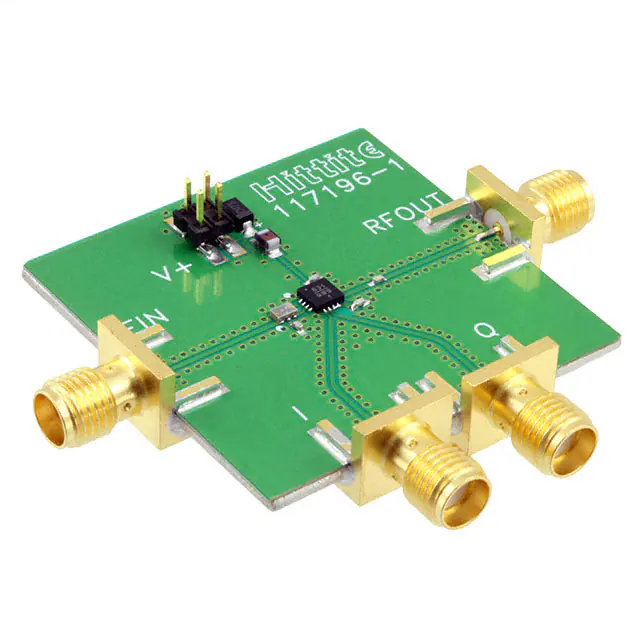
Evaluation PCB
MODULATORS - SMT
10
List of Materials for Evaluation PCB 117201 [1]
Item
Description
J1 - J4
PCB Mount SMA Connector
J5
2 mm DC Header
C1
4.7 μF Capacitor, Tantalum
C2 - C5
100 pF Capacitor, 0402 Pkg.
T1
Balun, 0805 Pkg.
ANAREN BD1722J50100A
L1
330 nH Inductor, 0805 Pkg.
U1
HMC631LP3(E) Vector Modulator
PCB [2]
117196 Evaluation PCB
The circuit board used in the final application should
use RF circuit design techniques. Signal lines
should have 50 ohm impedance while the package
ground leads and exposed paddle should be connected directly to the ground plane similar to that
shown. A sufficient number of via holes should be
used to connect the top and bottom ground planes.
The evaluation board should be mounted to an
appropriate heat sink. The evaluation circuit board
shown is available from Hittite upon request.
[1] Reference this number when ordering complete evaluation PCB
[2] Circuit Board Material: Rogers 4350, Er = 3.48
10 - 64
For price, delivery, and to place orders, please contact
Hittite
Microwave
Corporation:
For price,
delivery,
and to place
orders: Analog Devices, Inc.,
One Technology Way,
P.O. 978-250-3373
Box 9106, Norwood, MA 02062-9106
20 Alpha Road, Chelmsford, MA 01824 Phone: 978-250-3343
Fax:
Phone: 781-329-4700 • Order online at www.analog.com
Order On-line at www.hittite.com
Application Support: Phone: 1-800-ANALOG-D
Information furnished by Analog Devices is believed to be accurate and reliable. However, no
responsibility is assumed by Analog Devices for its use, nor for any infringements of patents or other
rights of third parties that may result from its use. Specifications subject to change without notice. No
license is granted by implication or otherwise under any patent or patent rights of Analog Devices.
Trademarks and registered trademarks are the property of their respective owners.
�HMC631LP3 / 631LP3E
v00.1007
GaAs HBT VECTOR
MODULATOR 1.8 - 2.7 MHz
Notes:
MODULATORS - SMT
10
For price, delivery, and to place orders, please contact
Hittite
Microwave
Corporation:
For price,
delivery,
and to place
orders: Analog Devices, Inc.,
One Technology Way,
P.O. 978-250-3373
Box 9106, Norwood, MA 02062-9106
20 Alpha Road, Chelmsford, MA 01824 Phone: 978-250-3343
Fax:
Phone: 781-329-4700 • Order online at www.analog.com
Order On-line at www.hittite.com
Application Support: Phone: 1-800-ANALOG-D
Information furnished by Analog Devices is believed to be accurate and reliable. However, no
responsibility is assumed by Analog Devices for its use, nor for any infringements of patents or other
rights of third parties that may result from its use. Specifications subject to change without notice. No
license is granted by implication or otherwise under any patent or patent rights of Analog Devices.
Trademarks and registered trademarks are the property of their respective owners.
10 - 65
�