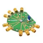
HMC940LC4B
v03.0322
High Speed Digital Logic - SMT
13 Gbps, 1:4 FANOUT BUFFER
w/ PROGRAMMABLE OUTPUT VOLTAGE
Typical Applications
Features
The HMC940LC4B is ideal for:
Inputs Terminated Internally in 50 Ohms
• RF ATE Applications
Differential Inputs are DC Coupled
• Broadband Test & Measurement
Propagation Delay: 101 ps
• Serial Data Transmission up to 13 Gbps
Fast Rise and Fall Times: 26 / 25 ps
• Clock Buffering up to 13 GHz
Programmable Differential
Output Voltage Swing: 600 - 1400 mV
Power Dissipation: 440 mW
24 Lead Ceramic 4x4 mm SMT Package: 16 mm 2
Functional Diagram
General Description
The HMC940LC4B is a 1:4 Fanout Buffer designed to
support data transmission rates up to 13 Gbps, and
clock frequencies as high as 13 GHz. All differential
inputs and outputs are DC coupled and terminated on
chip with 50 Ohm resistors to ground. The outputs may
be used in either single-ended or differential modes,
and should be AC or DC coupled into 50 Ohm resistors
connected to ground.
The HMC940LC4B also features an output level control
pin, VR which allows for loss compensation or for signal
level optimization. The HMC940LC4B operates from a
single -3.3V DC supply and is available in a ceramic
RoHS compliant 4x4 mm SMT package.
Electrical Specifications, TA = +25 ºC Vee = -3.3V, VR = 0V
Parameter
Conditions
Power Supply Voltage (Vee)
Typ.
Max
-3.6
-3.3
-3.0
Units
V
Power Supply Current
133
mA
Maximum Data Rate
13
Gbps
Maximum Clock Rate
13
GHz
Input High Voltage
-0.5
0.5
Input Low Voltage
-1.0
0.0
Input Return Loss
V
dB
Single-Ended, peak-to-peak
585
mVp-p
Differential, peak-to-peak
1170
mVp-p
Output High Voltage
-15
mV
Output Low Voltage
-600
mV
26 / 25
ps
Output Rise / Fall Time
Frequency
很抱歉,暂时无法提供与“126572-HMC940LC4B”相匹配的价格&库存,您可以联系我们找货
免费人工找货