HMC953LC4B
v01.0111
14 Gbps, DUAL D-TYPE FLIP-FLOP WITH COMMON CLOCK
& PROGRAMMABLE OUTPUT VOLTAGE
HIGH SPEED LOGIC - SMT
3
Typical Applications
Features
The HMC953LC4B is ideal for:
Supports High Data Rates: up to 14 Gbps
• 16G Fiber Channel
Differential or Single-Ended Operation
• Serial Data Transmission up to 14 Gbps
Fast Rise and Fall Times: 22 / 20 ps
• Digital Logic Systems up to 14 GHz
Low Power Consumption: 442 mW typ.
• Matched Delay Applications
Programmable Differential
Output Voltage Swing: 600 - 1300 mVp-p
• Broadband Test & Measurement
Propagation Delay: 104 ps
Single Supply: -3.3 V
24 Lead Ceramic 4x4 mm SMT Package: 16 mm2
Functional Diagram
General Description
The HMC953LC4B is a Differential Dual D-Type Flip
Flop with a common clock to support data transmission
rates of up to 14 Gbps, and clock port operation of up
to 14 GHz. During normal operation, dual differential
data is transferred to the respective outputs on the
positive edge of the clock. Reversing the clock inputs
allows for negative-edge triggered applications. The
HMC953LC4B also features an output level control
pin, VR, which allows for loss compensation or for
signal level optimization.
All differential input signals to the HMC953LC4B are
terminated with 50 Ohms to ground on-chip, and
may be either AC or DC coupled. The outputs of the
HMC953LC4B may be operated either differentially
or single-ended. Outputs can be connected directly
to a 50 Ohm terminated system, while DC blocking
capacitors may be used if the terminating system is
50 Ohms to a non-ground DC voltage. The HMC953LC4B operates from a single -3.3 V DC supply
and is available in a ceramic RoHS-compliant 4x4 mm
SMT package.
Electrical Specifications, TA = +25 °C, Vee = -3.3 V
Parameter
Conditions
Power Supply Voltage
Min.
Typ.
Max
Units
-3.6
-3.3
-3.0
V
Power Supply Current
134
mA
Maximum Data Rate
14
Gbps
Maximum Select Rate
GHz
-1.5
0.5
V
Input Differential Range
0.1
2.0
Vp-p
Input Return Loss
Output Amplitude
3-1
14
Input Voltage Range
Frequency H
H
X
X
L
L->H
X
L
X
H
L->H
X
H
H = Positive voltage level
L = Negative voltage level
Notes:
DX = DXP - DXN
C = CP - CN
QX = QXP - QXN
For price, delivery and to place orders: Hittite Microwave Corporation, 20 Alpha Road, Chelmsford, MA 01824
Phone: 978-250-3343
Fax: 978-250-3373
Order On-line at www.hittite.com
Application Support: Phone: 978-250-3343 or apps@hittite.com
HIGH SPEED LOGIC - SMT
Timing Diagram
3
3-4
�HMC953LC4B
v01.0111
14 Gbps, DUAL D-TYPE FLIP-FLOP WITH COMMON CLOCK
& PROGRAMMABLE OUTPUT VOLTAGE
Absolute Maximum Ratings
HIGH SPEED LOGIC - SMT
3
Power Supply Voltage (Vee)
-3.75 V to +0.5 V
Input Signals
-2.0 V to 0.5 V
Output Signals
-1.5 V to 0.5 V
Junction Temperature
125 °C
Continuous Pdiss (T = 85 °C
(derate 30.0 mW/°C above 85 °C)
1.22 W
Thermal Resistance (Rth j-p)
Worst case device to package paddle
32.8 °C/W
Storage Temperature
-65 °C to +150 °C
Operating Temperature
-40 to +85 °C
ELECTROSTATIC SENSITIVE DEVICE
OBSERVE HANDLING PRECAUTIONS
Outline Drawing
NOTES:
1. PACKAGE BODY MATERIAL: ALUMINA
2. LEAD AND GROUND PADDLE PLATING:
30-80 MICROINCHES GOLD OVER 50 MICROINCHES MINIMUM NICKEL.
3. DIMENSIONS ARE IN INCHES [MILLIMETERS].
4. LEAD SPACING TOLERANCE IS NON-CUMULATIVE.
5. PACKAGE WARP SHALL NOT EXCEED 0.05mm DATUM -C6. ALL GROUND LEADS MUST BE SOLDERED TO PCB RF GROUND.
7. PADDLE MUST BE SOLDERED TO Vee.
3-5
For price, delivery and to place orders: Hittite Microwave Corporation, 20 Alpha Road, Chelmsford, MA 01824
Phone: 978-250-3343
Fax: 978-250-3373
Order On-line at www.hittite.com
Application Support: Phone: 978-250-3343 or apps@hittite.com
�HMC953LC4B
v01.0111
14 Gbps, DUAL D-TYPE FLIP-FLOP WITH COMMON CLOCK
& PROGRAMMABLE OUTPUT VOLTAGE
Pin Descriptions
Function
Description
1, 6, 8, 11, 13, 18
GND
Signal Grounds.
2, 3,
4, 5
D1P, D1N,
D2P, D2N
Differential Inputs: Current Mode Logic (CML)
referenced to positive supply.
7, 12, 22
N/C
No connection necessary. These pins may be connected to
RF/DC ground without affecting performance.
9, 10
CP, CN
Differential Clock Inputs: Current Mode Logic (CML)
referenced to positive supply.
14, 15,
16, 17
Q2N, Q2P,
Q1N, Q1P
Differential Outputs: Current Mode Logic (CML)
referenced to positive supply.
19, 24
GND
Supply Ground
20, 23
Package Base
Vee
These pins and the exposed paddle must be
connected to the negative voltage supply.
21
VR
Output level control. Output level may be increased
or decreased by applying a voltage to VR per “Output
Differential vs. VR” plot.
Interface Schematic
For price, delivery and to place orders: Hittite Microwave Corporation, 20 Alpha Road, Chelmsford, MA 01824
Phone: 978-250-3343
Fax: 978-250-3373
Order On-line at www.hittite.com
Application Support: Phone: 978-250-3343 or apps@hittite.com
3
HIGH SPEED LOGIC - SMT
Pin Number
3-6
�HMC953LC4B
v01.0111
14 Gbps, DUAL D-TYPE FLIP-FLOP WITH COMMON CLOCK
& PROGRAMMABLE OUTPUT VOLTAGE
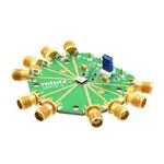
Evaluation PCB
HIGH SPEED LOGIC - SMT
3
List of Materials for Evaluation PCB 126572 [1]
Item
Description
J1 - J10
PCB Mount SMA RF Connectors
J15 - J18
DC Pin
JP1
0.1” Header with Shorting Jumper
C1, C2
4.7 µF Capacitor, Tantalum
C3 - C5
100 pF Capacitor, 0603 Pkg.
R1
10 Ohm Resistor, 0603 Pkg.
U1
HMC953LC4B Dual D-Type Flip Flop
PCB [2]
126570 Evaluation Board
[1] Reference this number when ordering complete evaluation PCB
[2] Circuit Board Material: Arlon 25FR or Rogers 4350
3-7
The circuit board used in the application should use
RF circuit design techniques. Signal lines should
have 50 Ohm impedance while the package ground leads should be connected directly to the
ground plane similar to that shown. The exposed
package base should be connected to Vee. A sufficient number of via holes should be used to connect
the top and bottom ground planes. The evaluation
circuit board shown is available from Hittite upon
request. Install jumper on JP1 to short VR to GND
for normal operation.
For price, delivery and to place orders: Hittite Microwave Corporation, 20 Alpha Road, Chelmsford, MA 01824
Phone: 978-250-3343
Fax: 978-250-3373
Order On-line at www.hittite.com
Application Support: Phone: 978-250-3343 or apps@hittite.com
�HMC953LC4B
v01.0111
14 Gbps, DUAL D-TYPE FLIP-FLOP WITH COMMON CLOCK
& PROGRAMMABLE OUTPUT VOLTAGE
Application Circuit
HIGH SPEED LOGIC - SMT
3
For price, delivery and to place orders: Hittite Microwave Corporation, 20 Alpha Road, Chelmsford, MA 01824
Phone: 978-250-3343
Fax: 978-250-3373
Order On-line at www.hittite.com
Application Support: Phone: 978-250-3343 or apps@hittite.com
3-8
�