FEATURES
FUNCTIONAL BLOCK DIAGRAM
13 VCCO
14 VEE
16 VCCI
15 RTN
HMC974LC3C
RT 1
11 WOUTB
WIT 3
10 URB
9 VCCO
VEE 8
RB 4
LE 7
Automatic test equipment (ATE)
High speed instrumentation
Clock and data restoration
Semiconductor test systems
Threshold detection in electronic warfare systems
WIN 2
LE 6
APPLICATIONS
12 ORB
PACKAGE
BASE
VEE
14863-001
Propagation delay: 88 ps
Propagation delay at 50 mV overdrive: 20 ps
Minimum detectable pulse width: 60 ps
Differential latch control
Power dissipation: 240 mW
16-terminal 2.9 mm × 2.9 mm LCC package
VCCI 5
Data Sheet
High Speed, 10 GHz Window Comparator
HMC974LC3C
Figure 1.
GENERAL DESCRIPTION
The HMC974LC3C is a silicon germanium (SiGe) monolithic,
ultra fast window comparator that features reduced swing
positive emitter-coupled logic (RSPECL) output drivers that are
level latched. Three output ports detect whether an analog input
signal is above, below, or between two reference levels supplied
at the input (see Figure 2).
Rev. E
The outputs are single-ended negative logic. Incorporating two
proven comparators at the input provides good dc and dynamic
matching and reduces the input capacitance. The reduced swing
output stages are designed to directly drive 400 mV into 50 Ω
terminated to a voltage (VTERM = VCCO − 2 V).
The HMC974LC3C features high speed latches that can either
be enabled to latch the output data or left in the track mode to
implement a tracking window comparator.
Document Feedback
Information furnished by Analog Devices is believed to be accurate and reliable. However, no
responsibility is assumed by Analog Devices for its use, nor for any infringements of patents or other
rights of third parties that may result from its use. Specifications subject to change without notice. No
license is granted by implication or otherwise under any patent or patent rights of Analog Devices.
Trademarks and registered trademarks are the property of their respective owners.
One Technology Way, P.O. Box 9106, Norwood, MA 02062-9106, U.S.A.
Tel: 781.329.4700
©2018 Analog Devices, Inc. All rights reserved.
Technical Support
www.analog.com
�HMC974LC3C
Data Sheet
TABLE OF CONTENTS
Features .............................................................................................. 1
Pin Configuration and Function Descriptions..............................6
Applications ....................................................................................... 1
Interface Schematics .....................................................................7
Functional Block Diagram .............................................................. 1
Typical Performance Characteristics ..............................................8
General Description ......................................................................... 1
Theory of Operation .........................................................................9
Revision History ............................................................................... 2
Power Sequencing .........................................................................9
Specifications..................................................................................... 3
Applications Information .............................................................. 10
Timing Diagram ........................................................................... 4
Evaluation Board ........................................................................ 10
Absolute Maximum Ratings............................................................ 5
Outline Dimensions ....................................................................... 12
ESD Caution .................................................................................. 5
Ordering Guide .......................................................................... 12
REVISION HISTORY
4/2018—Rev. D to Rev. E
Changes to WOUTB Parameter, Unit Column, Table 1 and URB
and ORB Parameter, Unit Column, Table 1 .................................. 3
Changes to Ordering Guide .......................................................... 12
6/2017—Rev. C to Rev. D
Changes to Table 1 ............................................................................ 3
Added Maximum Peak Reflow Temperature Parameter,
Table 2 ................................................................................................ 5
Updated Outline Dimensions ....................................................... 12
Changes to Ordering Guide .......................................................... 12
This Hittite Microwave Products data sheet has been reformatted
to meet the styles and standards of Analog Devices, Inc.
3/2017—v04.0616 to Rev. C
Updated Format .................................................................. Universal
Changes to General Description .....................................................1
Changes to Table 1.............................................................................3
Added Negative Supply (VEE to GND) Parameter, Table 2 ..........5
Changes to Table 3.............................................................................5
Added Theory of Operation Section, Power Sequencing Section,
and Table 4..........................................................................................9
Added Applications Information Section
Changes to Evaluation Board Section and Table 5 .................... 10
Updated Outline Dimensions ....................................................... 12
Changes to Ordering Guide .......................................................... 12
Rev. E | Page 2 of 12
�Data Sheet
HMC974LC3C
SPECIFICATIONS
TA = 25°C, VEE = −3 V, VCCI = 3.3 V, VCCO = 2 V, VTERM = 0 V, VCM = 0 V, VOD = 50 mV. VOD is the input overdrive voltage, for example,
VWIN − VRT = VOD or VWIN − VRB = VOD.
Table 1.
Parameter
DC INPUT CHARACTERISTICS
Offset Voltage
Bias Current
Differential Voltage
Input Impedance
WIN Pin to WIT Pin
RT Pin to WIT Pin
RB Pin to WIT Pin
Common-Mode Input Voltage Range
Input Capacitance
LATCH ENABLE CHARACTERISTICS
LE and LE
Input Low Voltage (VIL)
Input High Voltage (VIH)
LE and LE Impedance
DC OUTPUT CHARACTERISTICS
Output Voltage
High Level, VOH (50 Ω to 0 V)
Low Level, VOL (50 Ω to 0 V)
Output Voltage Swing
WOUTB
URB and ORB
AC PERFORMANCE
Propagation Delay Dispersion vs. VOD
Rise Time (ORB, WOUTB, URB), tR
Fall Time (ORB, WOUTB, URB), tF
Minimum Detectable Pulse Width
Equivalent Input Bandwidth1
Input to Output Delay, tPD
Latch to Output Delay, tPD
Maximum Input Slew Rate
Noise (Referred to Input)
Random Jitter (rms)
Deterministic Jitter (Peak to Peak)
POWER SUPPLIES (INCLUDING LOAD)
Positive Supply Voltage Input Stage (VCCI)
Positive Supply Voltage Output Stage (VCCO)
Negative Power Supply (VEE)
Positive Supply Current Input Stage (ICCI)
Positive Supply Current Output Stage (ICCO)
Negative Current (IEE)
Power Dissipation (PD)
1
Min
Typ
Max
Unit
−10
−30
−2
±4
+20
+10
+30
+2
mV
μA
V
+1.5
1
Ω
Ω
Ω
V
pF
50
50
50
−1.5
1.6
7.8
V
V
kΩ
1.06
0.73
V
V
2.2
300
320
360
380
420
440
20
25.3
21.9
60
11
88
83
5
6
0.2
2
3.135
1.8
−3.15
10
60
21
3.3
3.3
−3.0
15
70
31
240
WIT pin termination open
Measured between the WIN pin voltage and the
RT pin voltage or RB pin voltage
WIT to GND
If not driven, the device is unlatched
mV
mV
ps
ps
ps
ps
GHz
ps
ps
V/ns
nV/√(Hz)
ps rms
ps
3.465
3.465
−2.85
20
80
41
Test Conditions/Comments
For VOD > 50 mV
20% to 80%
80% to 20%
VCM = 0 V; ±100 mV overdrive voltage
At 5 Gbps with ±100 mV overdrive
At 5 Gbps with ±100 mV overdrive
V
V
V
mA
mA
mA
mW
Equivalent input bandwidth is calculated with the following formula: BWEQ = 0.22⁄√(TRCOMP2 − TRIN2), where BWEQ is the equivalent bandwidth formula, TRIN is the 20% to
80% transition time of a quasi Gaussian signal applied to the comparator input, and TRCOMP is the effective transition time digitized by the comparator.
Rev. E | Page 3 of 12
�HMC974LC3C
Data Sheet
TIMING DIAGRAM
RT
RB
WIN
LATCH
LATCH
LE, LE
TRACK
tPD (LE TO OUT)_ORB
tPD (IN TO OUT)_ORB
ORB
tPD (IN TO OUT)_WOUTB_H TO L
tPD (IN TO OUT)_WOUTB_L TO H
WOUTB
tPD (IN TO OUT)_URB_L TO H
tPD (IN TO OUT)_URB_H TO L
tF
tR
Figure 2. Timing Diagram
Rev. E | Page 4 of 12
14863-002
URB
�Data Sheet
HMC974LC3C
ABSOLUTE MAXIMUM RATINGS
Table 2.
Parameter
Input Supply Voltage (VCCI to GND)
Output Supply Voltage (VCCO to GND)
Positive Supply Differential (VCCI − VCCO)
Negative Supply (VEE to GND)
Input Voltage
Differential Input Voltage
Output Current
Junction Temperature
Continuous Power Dissipation (T = 85°C;
Derate 20.4 mW/°C Above 85°C)
Thermal Resistance (θJC)
Maximum Peak Reflow Temperature1
Moisture Sensitivity Level 1 (MSL1) and
Moisture Sensitivity Level 3 (MSL3)
Storage Temperature Range
Operating Temperature Range
Electrostatic Discharge (ESD) Sensitivity
Human Body Model
1
Rating
−0.5 V to +4 V
−0.5 V to +4 V
−0.5 V to +3 V
−3.3 V to +0.5 V
−2 V to +2 V
−2 V to +2 V
40 mA
125°C
0.816 W
Stresses at or above those listed under Absolute Maximum
Ratings may cause permanent damage to the product. This is a
stress rating only; functional operation of the product at these
or any other conditions above those indicated in the operational
section of this specification is not implied. Operation beyond
the maximum operating conditions for extended periods may
affect product reliability.
ESD CAUTION
49°C/W
260°C
−65°C to +150°C
−40°C to +85°C
Class 1B
See the Ordering Guide section.
Rev. E | Page 5 of 12
�HMC974LC3C
Data Sheet
13 VCCO
14 VEE
15 RTN
16 VCCI
PIN CONFIGURATION AND FUNCTION DESCRIPTIONS
RT 1
12 ORB
WIN 2
11 WOUTB
HMC974LC3C
TOP VIEW
(Not to Scale)
WIT 3
10 URB
PACKAGE
BASE
NOTES
1. EXPOSED PAD. THE EXPOSED PAD MUST
BE CONNECTED TO VEE .
VEE
14863-003
VEE 8
LE 7
LE 6
9 VCCO
VCCI 5
RB 4
Figure 3. Pin Configuration
Table 3. Pin Function Descriptions
Pin No.
1
2
3
4
5, 16
6
7
8, 14
9, 13
10
11
Mnemonic
RT
WIN
WIT
RB
VCCI
LE
LE
VEE
VCCO
URB
WOUTB
12
15
ORB
RTN
EPAD
Description
Termination Resistor for Reference Top.
Analog Input Window.
Common Mode Window for Termination Resistors.
Termination Resistor Return for Reference Bottom.
Positive Supply Voltage Input Stage.
Inverting Latch Enable Input.
Noninverting Latch Enable Input.
Negative Power Supply
Positive Supply Voltage Output Stage.
Underange Output. URB is asserted low when the analog input voltage is below the RB pin voltage.
Window Output. WOUTB is asserted low when the analog input voltage is between the RB pin voltage and the
RT pin voltage.
Overrange output. ORB is asserted low when the analog input voltage range is above the RT pin voltage.
ESD Protection Return.
Exposed Pad. The exposed pad must be connected to VEE.
Rev. E | Page 6 of 12
�Data Sheet
HMC974LC3C
INTERFACE SCHEMATICS
VCCO
RT
50Ω
50Ω
URB,
WOUTB,
ORB
14863-004
WIT
50Ω
RB
Figure 4. Interface Schematic for RT, RB, WIN, and WIT
Figure 6. Interface Schematic for URB, WOUTB, and ORB
VCCI
14863-005
LE, LE
VEE
14863-006
WIN
Figure 5. Interface Schematic for LE and LE
Rev. E | Page 7 of 12
�HMC974LC3C
Data Sheet
TYPICAL PERFORMANCE CHARACTERISTICS
1.5
75
VCM = +0.5V
VCM = 0V
VCM = –0.5V
1.3
VOL/VOH LEVELS (V)
45
30
15
1.1
0.9
0.7
0
0
10
20
30
40
50
60
70
80
90
100
110
OVERDRIVE VOLTAGE (mV)
0.5
–45
14863-007
–15
–19
–6
7
20
33
46
59
72
85
TEMPERATURE (°C)
Figure 7. Dispersion vs. Overdrive Voltage
Figure 10. VOL/VOH Levels vs. Temperature
80
0.62
ORB SWING
WOUT SWING
URB SWING
70
0.54
VCCI
VCCO
VEE
60
CURRENT (mA)
OUTPUT VOLTAGE SWING (V)
–32
14863-010
DISPERSION (ps)
60
ORB, VOH
WOUT, VOH
URB, VOH
ORB, VOL
WOUT, VOL
URB, VOL
0.46
50
40
30
0.38
–32
–19
–6
7
20
33
46
59
72
85
TEMPERATURE (°C)
Figure 8. Output Voltage Swing vs. Temperature
ORB, RISE
WOUT, RISE
URB, RISE
ORB, FALL
WOUT, FALL
URB, FALL
30
28
26
24
22
20
–45
–32
–19
–6
7
20
33
46
TEMPERATURE (°C)
59
72
85
14863-009
DELAY (ps)
32
–32
–19
–6
7
20
33
46
TEMPERATURE (°C)
Figure 11. Power Supply Currents
36
34
10
–45
Figure 9. Output Rise and Fall Time
Rev. E | Page 8 of 12
59
72
85
14863-011
0.30
–45
14863-008
20
�Data Sheet
HMC974LC3C
THEORY OF OPERATION
The HMC974LC3C is a window comparator where the range of
the window is defined with RT as the top of the voltage window
range and RB as the bottom of the voltage window range. The
comparator has two modes of operation: track mode and latch
mode. While in track mode, the comparator determines three
things:
1.
2.
3.
If the signal is below the window voltage value, RT, and
above the window voltage value, RB, represented by the
WOUTB output.
If the signal is above the window voltage value RT, which is
represented by the ORB output.
If the signal is below the window voltage value RB, which is
represented by the URB output.
A typical 5 Gbps output eye is shown in Figure 12 with specific
details outlined in Table 4.
Table 4. Eye Diagram Details
Parameter
Bit Rate
Pattern Length
Deterministic Jitter (Peak-to-Peak)
Vertical Scale
Time Scale
POWER SEQUENCING
Use the following supplies sequentially to power up the device:
1.
2.
3.
VCCO (if different than ground)
VCCI and VCCO (if VCCO = VCCI)
VEE
Apply power to the HMC974LC3C before applying the input
signals (WIN and WIT) and remove the input signals (WIN and
WIT) prior to powering it down.
EDGE SAMPLES
14863-012
VOLTAGE (80mV/DIV)
VEE
VCCI and VCCO (if VCCO = VCCI)
VCCO (if different than ground)
The power-down sequence is the reverse of the previous
sequence:
1.
2.
3.
TIME (33.3ps/DIV)
Value
5 Gbps
215 − 1
2.15 ps
80 mV/div
33.3 ps/div
Figure 12. Eye Diagram at 5 Gbps
Rev. E | Page 9 of 12
�HMC974LC3C
Data Sheet
APPLICATIONS INFORMATION
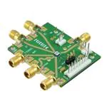
EVALUATION BOARD
Table 5. Bill of Materials
The HMC974LC3C evaluation printed circuit board (PCB)
must use RF circuit design techniques. Signal lines must have
50 Ω impedance while the package ground leads must connect
directly to the ground plane of the PCB. The exposed metal
package base must connect to VEE. Ensure the top and bottom
ground planes connect together with via holes. The evaluation
PCB shown in Figure 13 is available from Analog Devices, Inc.,
upon request.
Reference Designator
J1
J2 to J7
J8
JP1, JP2
C1 to C3, C5, C6, C8 to C10,
C15
C4, C7, C11
C12 to C14
TP1 to TP4
U1
PCB
330 pF capacitor, 0402
4.7 μF tantalum capacitor
DC pin
HMC974LC3C window comparator
EVAL-HMC974LC3C evaluation
board, circuit board material is
either Rogers 4350 or Arlon 25FR
14863-013
Figure 14 shows the EVAL-HMC974LC3C schematic. Figure 15
shows the typical application circuit.
Description
Eight-position vertical header
K connector, SRI
Terminal strip, single row, 3-pin
Two position vertical header
100 pF capacitor, 0402
Figure 13. Evaluation Printed Circuit Board
Rev. E | Page 10 of 12
�Data Sheet
HMC974LC3C
TP4
C6
100pF
16
C8
100pF
2
11
J4
WOUTB
3
10
J5
URB
JP3
C9
100pF
4
9
J1
VCCO
C3
100pF
J8
8
C1
100pF
J1
VCCO
C14
4.7µF
J3
ORB
5
TP3
RB
JP2
C11
330pF
12
J2-WIN
TP2-WIT
C2
100pF
J1
VEE
1
7
JP1
6
TP1
RT
C12
4.7µF
13
C5
100pF
14
C7
330pF
C13
4.7µF
15
J1
VCCI
C4
330pF
GND
PACKAGE
BASE
J1
VCCI
VEE
VEE
C10
100pF
J6
LE
J1
VEE
C15
100pF
J7
LE
1
2
3
4
5
6
7
8
J1
GND
VEE
SLUG
VCC0
Figure 14. Evaluation Board Schematic
VCCI = +3.3V
VCCO = +2.0V
ORB,
WOUTB,
URB
OSCILLOSCOPE INPUT
50Ω
VCM_OUT
~0.9V
50Ω
HMC974 10GHz
WINDOW COMPARATOR
GND
14863-015
VCCI
VEE
14863-014
JP8
VEE = –3.0V
Figure 15. Typical Application Circuit
Rev. E | Page 11 of 12
�HMC974LC3C
Data Sheet
OUTLINE DIMENSIONS
3.05
2.90 SQ
2.75
PIN 1
INDICATOR
0.36
0.30
0.24
0.08
BSC
PIN 1
16
13
1
12
0.50
BSC
1.60
1.50 SQ
1.40
EXPOSED
PAD
9
4
5
8
0.32
BSC
TOP VIEW
1.50
REF
2.10 BSC
SIDE VIEW
FOR PROPER CONNECTION OF
THE EXPOSED PAD, REFER TO
THE PIN CONFIGURATION AND
FUNCTION DESCRIPTIONS
SECTION OF THIS DATA SHEET.
SEATING
PLANE
02-24-2017-C
PKG-004838
0.90
0.80
0.70
BOTTOM VIEW
Figure 16. 16-Terminal Ceramic Leadless Chip Carrier [LCC]
(E-16-1)
Dimensions shown in millimeters
ORDERING GUIDE
Model1
HMC974LC3C
HMC974LC3CTR
HMC974LC3CTR-R5
129538-HMC974LC3C
1
2
3
Temperature Range
−40°C to +85°C
−40°C to +85°C
−40°C to +85°C
MSL Rating2
MSL3
MSL3
MSL3
Package Description3
16-Terminal Ceramic Leadless Chip Carrier [LCC]
16-Terminal Ceramic Leadless Chip Carrier [LCC]
16-Terminal Ceramic Leadless Chip Carrier [LCC]
Evaluation Board
The HMC974LC3C, the HMC974LC3CTR, and the HMC974LC3CTR-R5 are RoHS Compliant Parts.
See the Absolute Maximum Ratings section.
Alumina and white package body material with a gold over nickel lead finish.
©2018 Analog Devices, Inc. All rights reserved. Trademarks and
registered trademarks are the property of their respective owners.
D14863-0-4/18(E)
Rev. E | Page 12 of 12
Package Option
E-16-1
E-16-1
E-16-1
�