HMC972LP5E
v00.1210
GaAs MMIC ANALOG VARIABLE
GAIN AMPLIFIER, 0.5 - 6.0 GHz
Typical Applications
Features
The HMC972LP5E is ideal for:
Wide Gain Control Range: -35 to +15 dB
• Cellular/3G Infrastructure
High Output IP3: +28 dBm
• WiBro / WiMAX / 4G
Positive Analog Control: 0 to +5V
• Microwave Radio & VSAT
Can be configured with 1 or 2 Attenuators
32 Lead 5x5 mm SMT Package: 25 mm2
• Test Equipment and Sensors
TE
• IF & RF Applications
General Description
Functional Diagram
The HMC972LP5E is an analog controlled variable
gain amplifier composed of two identical voltage
variable attenuators in combination with an InGaP
HBT gain block MMIC amplifier which operates
from 0.5 to 6 GHz, and can be controlled to provide
anywhere from 15 dB of gain to 35 dB of attenuation.
The HMC972LP5E delivers noise figure of 7.5 dB in
its maximum gain state, with output IP3 of up to
+28 dBm. The HMC972LP5E is housed in a RoHS
compliant 5x5 mm QFN leadless package, and requires no external matching components.
13 - 1
LE
B
SO
Electrical Specifications, TA = +25° C, 50 Ohm System, Vdd = ATT1Vdd = ATT2Vdd = +5V [1]
Parameter
Frequency
Min.
Typ.
Insertion Gain (Vctl = 0V)
0.5 - 2.7 GHz
2.7 - 4.0 GHz
4.0 - 6.0 GHz
10.5
6
13
9
0
dB
dB
Gain Control Range
0.5 - 4.0 GHz
4.0 - 6.0 GHz
50
42
dB
12
dB
O
Variable gain amplifiers - ANALOG - SMT
13
Input Return Loss (Vctl = 0V)
Output Return Loss (Vctl = 0V)
Max.
Units
10
dB
Output Power for 1dB Compression (Vctl = 0V)
0.5 - 2.7 GHz
2.7 - 4.0 GHz
4.0 - 6.0 GHz
16
13
6
dBm
dBm
Output Third Order Intercept Point
(Two-Tone Output Power= 0 dBm Each Tone) (Vctl = 0V)
0.5 - 2.7 GHz
2.7 - 4.0 GHz
4.0 - 6.0 GHz
29
26
20
dBm
dBm
7.5
dB
Noise Figure (Vctl = 0V)
Idd
85
102
mA
ATT1Idd
75
0.2
0.3
mA
ATT2Idd
0.2
0.3
mA
[1] Unless otherwise noted, test conditions: ATT1 + AMP + ATT2 in cascade.
For price,
delivery,
and to placeCorporation:
orders: Analog Devices, Inc.,
For price, delivery, and to place orders, please contact
Hittite
Microwave
One Technology Way, P.O. Box 9106, Norwood, MA 02062-9106
20 Alpha Road, Chelmsford, MA 01824 Phone: Phone:
978-250-3343
978-250-3373
781-329-4700Fax:
• Order
online at www.analog.com
Application Support: Phone: 1-800-ANALOG-D
Order On-line at www.hittite.com
Information furnished by Analog Devices is believed to be accurate and reliable. However, no
responsibility is assumed by Analog Devices for its use, nor for any infringements of patents or other
rights of third parties that may result from its use. Specifications subject to change without notice. No
license is granted by implication or otherwise under any patent or patent rights of Analog Devices.
Trademarks and registered trademarks are the property of their respective owners.
�HMC972LP5E
v00.1210
GaAs MMIC ANALOG VARIABLE
GAIN AMPLIFIER, 0.5 - 6.0 GHz
Gain vs. Frequency Over Vctl [1]
Gain Over Temperature (Vctl = 0V) [1]
20
20
10
15
0
GAIN (dB)
-20
-30
-40
-50
-60
-70
5
+25 C
+85 C
-40 C
0
-80
-5
1
2
3
4
5
0
6
FREQUENCY (GHz)
1
2
3
LE
Gain vs. Vctl Over Temperature @ 0.5 GHz [1]
20
5
6
13
Gain vs. Vctl Over Temperature @ 2 GHz [1]
20
10
+25 C
+85 C
-40 C
-10
-20
-30
-40
0
10
1
2
3
4
+25 C
+85 C
-40 C
0
B
SO
0
-10
-20
-30
-40
5
0
1
2
Vctl (V)
O
Gain vs. Vctl Over Temperature @ 4 GHz [1]
3
4
5
Vctl (V)
Gain vs. Vctl Over Temperature @ 6 GHz [1]
10
10
0
0
+25 C
+85 C
-40 C
+25 C
+85 C
-40 C
-10
GAIN (dB)
-10
GAIN (dB)
4
FREQUENCY (GHz)
-20
-30
-20
-30
-40
-40
-50
-50
0
1
2
3
4
5
Vctl (V)
0
1
2
3
4
5
Vctl (V)
[1] ATT1 + AMP + ATT2
For price,
delivery,
and to placeCorporation:
orders: Analog Devices, Inc.,
For price, delivery, and to place orders, please contact
Hittite
Microwave
One Technology Way, P.O. Box 9106, Norwood, MA 02062-9106
20 Alpha Road, Chelmsford, MA 01824 Phone: Phone:
978-250-3343
978-250-3373
781-329-4700Fax:
• Order
online at www.analog.com
Application Support: Phone: 1-800-ANALOG-D
Order On-line at www.hittite.com
Information furnished by Analog Devices is believed to be accurate and reliable. However, no
responsibility is assumed by Analog Devices for its use, nor for any infringements of patents or other
rights of third parties that may result from its use. Specifications subject to change without notice. No
license is granted by implication or otherwise under any patent or patent rights of Analog Devices.
Trademarks and registered trademarks are the property of their respective owners.
variable gain amplifiers - ANALOG - SMT
0
GAIN (dB)
10
TE
0.0 V
1.0 V
1.6 V
2.0 V
2.6 V
3.4 V
GAIN (dB)
GAIN (dB)
-10
13 - 2
�HMC972LP5E
v00.1210
GaAs MMIC ANALOG VARIABLE
GAIN AMPLIFIER, 0.5 - 6.0 GHz
Input Return Loss Over
Temperature (Vctl = 0V) [1]
0
-10
-10
RETURN LOSS (dB)
0
0.0 V
1.0 V
2.0 V
3.0 V
-30
-40
1
13
2
3
4
5
6
0
FREQUENCY (GHz)
2
3
4
5
6
5
6
LE
Output Return Loss Over
Temperature (Vctl = 0V) [1]
0
0
-10
-20
B
SO
RETURN LOSS (dB)
1
FREQUENCY (GHz)
Output Return Loss Over Vctl [1]
0.0 V
1.0 V
2.0 V
3.0 V
-30
-40
0
1
2
3
4
5
-10
-20
+25C
+85C
-40C
-30
-40
6
0
1
FREQUENCY (GHz)
2
3
4
FREQUENCY (GHz)
Output IP3 vs. Temperature (Vctl = 0V) [1]
O
Output IP3 vs. Vctl [1]
40
40
30
30
IP3 (dBm)
20
IP3 (dBm)
Variable gain amplifiers - ANALOG - SMT
+25C
+85C
-40C
-30
-40
0
13 - 3
-20
TE
-20
RETURN LOSS (dB)
RETURN LOSS (dB)
Input Return Loss Over Vctl [1]
10
0
0.0 V
1.0 V
1.6 V
2.0 V
3.4 V
-10
-20
20
+25 C
+85 C
-40 C
10
0
-30
0
1
2
3
4
5
6
FREQUENCY (GHz)
0
1
2
3
4
5
6
FREQUENCY (GHz)
[1] ATT1 + AMP + ATT2
For price,
delivery,
and to placeCorporation:
orders: Analog Devices, Inc.,
For price, delivery, and to place orders, please contact
Hittite
Microwave
One Technology Way, P.O. Box 9106, Norwood, MA 02062-9106
20 Alpha Road, Chelmsford, MA 01824 Phone: Phone:
978-250-3343
978-250-3373
781-329-4700Fax:
• Order
online at www.analog.com
Application Support: Phone: 1-800-ANALOG-D
Order On-line at www.hittite.com
Information furnished by Analog Devices is believed to be accurate and reliable. However, no
responsibility is assumed by Analog Devices for its use, nor for any infringements of patents or other
rights of third parties that may result from its use. Specifications subject to change without notice. No
license is granted by implication or otherwise under any patent or patent rights of Analog Devices.
Trademarks and registered trademarks are the property of their respective owners.
�HMC972LP5E
v00.1210
GaAs MMIC ANALOG VARIABLE
GAIN AMPLIFIER, 0.5 - 6.0 GHz
Output IP2 vs. Temperature (Vctl = 0V) [1]
Output IP2 vs. Vctl [1]
70
70
60
60
50
50
30
IP2 (dBm)
20
10
0
-10
-30
30
20
0.0 V
1.0 V
1.6 V
2.0 V
3.4 V
-20
40
TE
+25 C
+85 C
-40 C
10
-40
0
0
1
2
3
4
5
6
0
FREQUENCY (GHz)
1
2
3
4
5
6
13
FREQUENCY (GHz)
Output P1dB Over Temperature
(Vctl = 0V) [1]
LE
Noise Figure Over Temperature
(Vctl = 0V) [1]
15
20
B
SO
NF (dB)
5
+25 C
+85 C
-40 C
0
0
1
2
3
4
5
6
10
+25 C
+85 C
-40 C
5
0
0
1
2
3
4
5
6
FREQUENCY (GHz)
O
FREQUENCY (GHz)
P1dB (dBm)
15
10
[1] ATT1 + AMP + ATT2
For price,
delivery,
and to placeCorporation:
orders: Analog Devices, Inc.,
For price, delivery, and to place orders, please contact
Hittite
Microwave
One Technology Way, P.O. Box 9106, Norwood, MA 02062-9106
20 Alpha Road, Chelmsford, MA 01824 Phone: Phone:
978-250-3343
978-250-3373
781-329-4700Fax:
• Order
online at www.analog.com
Application Support: Phone: 1-800-ANALOG-D
Order On-line at www.hittite.com
Information furnished by Analog Devices is believed to be accurate and reliable. However, no
responsibility is assumed by Analog Devices for its use, nor for any infringements of patents or other
rights of third parties that may result from its use. Specifications subject to change without notice. No
license is granted by implication or otherwise under any patent or patent rights of Analog Devices.
Trademarks and registered trademarks are the property of their respective owners.
variable gain amplifiers - ANALOG - SMT
IP2 (dBm)
40
13 - 4
�HMC972LP5E
v00.1210
GaAs MMIC ANALOG VARIABLE
GAIN AMPLIFIER, 0.5 - 6.0 GHz
Insertion Loss vs. Temperature [2]
Insertion Loss vs. Vctl [2]
0
0
INSERTION LOSS (dB)
-20
-30
-40
0
2
4
13
6
0
8
2
3
4
5
6
7
LE
Input Return Loss vs. Vctl [2]
Output Return Loss vs. Vctl [2]
0
0
-10
-20
B
SO
RETURN LOSS (dB)
1
FREQUENCY (GHz)
FREQUENCY (GHz)
0.0 V
1.0 V
2.0 V
3.0 V
-30
-40
0
2
4
6
-10
-20
0.0 V
1.0 V
2.0 V
3.0 V
-30
-40
8
0
2
4
FREQUENCY (GHz)
50
50
40
40
IP3 (dBm)
60
30
10
0.5
0.0 V
1.0 V
1.6 V
2.0 V
2.6 V
3.4 V
1.5
2.5
3.5
8
Input IP3 vs. Temperature (Vctl = 0V) [2]
60
20
6
FREQUENCY (GHz)
O
Input IP3 vs. Vctl [2]
IP3 (dBm)
Variable gain amplifiers - ANALOG - SMT
+25 C
+85 C
-40 C
-10
-15
-50
13 - 5
-5
TE
0.0 V
1.0 V
1.6 V
2.0 V
2.6 V
3.4 V
RETURN LOSS (dB)
ATTENUATION (dB)
-10
4.5
30
+25 C
+85 C
-40 C
20
5.5
6.5
7.5
FREQUENCY (GHz)
10
0.5
1.5
2.5
3.5
4.5
5.5
6.5
7.5
FREQUENCY (GHz)
[2] ATT1 Only
For price,
delivery,
and to placeCorporation:
orders: Analog Devices, Inc.,
For price, delivery, and to place orders, please contact
Hittite
Microwave
One Technology Way, P.O. Box 9106, Norwood, MA 02062-9106
20 Alpha Road, Chelmsford, MA 01824 Phone: Phone:
978-250-3343
978-250-3373
781-329-4700Fax:
• Order
online at www.analog.com
Application Support: Phone: 1-800-ANALOG-D
Order On-line at www.hittite.com
Information furnished by Analog Devices is believed to be accurate and reliable. However, no
responsibility is assumed by Analog Devices for its use, nor for any infringements of patents or other
rights of third parties that may result from its use. Specifications subject to change without notice. No
license is granted by implication or otherwise under any patent or patent rights of Analog Devices.
Trademarks and registered trademarks are the property of their respective owners.
�HMC972LP5E
v00.1210
GaAs MMIC ANALOG VARIABLE
GAIN AMPLIFIER, 0.5 - 6.0 GHz
Bias Voltage
Absolute Maximum Ratings
RF Input Power
+12 dBm
Vdd (V)
Idd (Typ.) (mA)
Supply Voltage
5.5 Vdc
+5V
90
Channel Temperature
150 °C
Continuous Pdiss (T = 85 °C)
(derate 8.5 mW/°C above 85 °C) [1]
0.55 W
Thermal Resistance
(Junction to Exposed Ground Paddle)
120 °C/W
Storage Temperature
-65 to +150 °C
B
SO
Outline Drawing
NOTES:
1. PACKAGE BODY MATERIAL: ALUMINA
O
2. LEAD AND GROUND PADDLE PLATING: 30-80 MICROINCHES GOLD OVER
50 MICROINCHES MINIMUM NICKEL.
3. DIMENSIONS ARE IN INCHES [MILLIMETERS].
4. LEAD SPACING TOLERANCE IS NON-CUMULATIVE
5. PACKAGE WARP SHALL NOT EXCEED 0.05mm DATUM -C6. ALL GROUND LEADS AND GROUND PADDLE MUST BE SOLDERED
TO PCB RF GROUND.
7. CLASSIFIED AS MOISTURE SENSITIVITY LEVEL (MSL) 1.
Package Information
Part Number
Package Body Material
Lead Finish
HMC972LP5E
RoHS-compliant Low Stress Injection Molded Plastic
100% matte Sn
MSL Rating
MSL1
[2]
Package Marking [1]
H972
XXXX
[1] 4-Digit lot number XXXX
[2] Max peak reflow temperature of 260 °C
For price,
delivery,
and to placeCorporation:
orders: Analog Devices, Inc.,
For price, delivery, and to place orders, please contact
Hittite
Microwave
One Technology Way, P.O. Box 9106, Norwood, MA 02062-9106
20 Alpha Road, Chelmsford, MA 01824 Phone: Phone:
978-250-3343
978-250-3373
781-329-4700Fax:
• Order
online at www.analog.com
Application Support: Phone: 1-800-ANALOG-D
Order On-line at www.hittite.com
Information furnished by Analog Devices is believed to be accurate and reliable. However, no
responsibility is assumed by Analog Devices for its use, nor for any infringements of patents or other
rights of third parties that may result from its use. Specifications subject to change without notice. No
license is granted by implication or otherwise under any patent or patent rights of Analog Devices.
Trademarks and registered trademarks are the property of their respective owners.
13
variable gain amplifiers - ANALOG - SMT
Class 1A
TE
-40 to +85 °C
ESD Sensitivity (HBM)
LE
Operating Temperature
ELECTROSTATIC SENSITIVE DEVICE
OBSERVE HANDLING PRECAUTIONS
13 - 6
�HMC972LP5E
v00.1210
GaAs MMIC ANALOG VARIABLE
GAIN AMPLIFIER, 0.5 - 6.0 GHz
Pin Descriptions
12
ATT2OUT
This port is matched to 50 Ohms.
Blocking capacitor required.
13
Vctl
Attenuation control voltage for the attenuators.
0V for minimum attenuation, 5V for maximum attenuation.
15
ATT2VDD
Power Supply for attenuator 2. External bypass
capacitor is required. See application circuit.
16
ATT2IN
This port is matched to 50 Ohms. Blocking capacitor required.
Attenuator performance is similar to HMC973LP3E
21
AMPOUT
This port is matched to 50 Ohms. External Choke
inductor and DC blocking capacitor are required.
See application circuit.
24
GND
This pin and the exposed ground paddle
must be connected to RF/DC ground.
26
AMPIN
This port is matched to 50 Ohms. Blocking capacitor required.
Amplifier performance is similar to HMC589ST89E.
28
ATT1OUT
This port is matched to 50 Ohms.
Blocking capacitor required.
31
ATT1VDD
Power supply for attenuator 1. External bias capacitor is
required. See application circuit.
32
ATT1IN
This port is matched to 50 Ohms. Blocking capacitor required.
Attenuator performance is similar to HMC973LP3E
LE
TE
N/C
Interface Schematic
O
Variable gain amplifiers - ANALOG - SMT
13 - 7
Description
No connection required. The pins are not connected internally;
however, all data shown herein was measured with these pins
connected to RF/DC ground externally.
B
SO
Pin Number
13
Function
1 - 11, 14, 17 - 20,
22, 23, 25, 27,
29, 30
For price,
delivery,
and to placeCorporation:
orders: Analog Devices, Inc.,
For price, delivery, and to place orders, please contact
Hittite
Microwave
One Technology Way, P.O. Box 9106, Norwood, MA 02062-9106
20 Alpha Road, Chelmsford, MA 01824 Phone: Phone:
978-250-3343
978-250-3373
781-329-4700Fax:
• Order
online at www.analog.com
Application Support: Phone: 1-800-ANALOG-D
Order On-line at www.hittite.com
Information furnished by Analog Devices is believed to be accurate and reliable. However, no
responsibility is assumed by Analog Devices for its use, nor for any infringements of patents or other
rights of third parties that may result from its use. Specifications subject to change without notice. No
license is granted by implication or otherwise under any patent or patent rights of Analog Devices.
Trademarks and registered trademarks are the property of their respective owners.
�HMC972LP5E
v00.1210
GaAs MMIC ANALOG VARIABLE
GAIN AMPLIFIER, 0.5 - 6.0 GHz
For price,
delivery,
and to placeCorporation:
orders: Analog Devices, Inc.,
For price, delivery, and to place orders, please contact
Hittite
Microwave
One Technology Way, P.O. Box 9106, Norwood, MA 02062-9106
20 Alpha Road, Chelmsford, MA 01824 Phone: Phone:
978-250-3343
978-250-3373
781-329-4700Fax:
• Order
online at www.analog.com
Application Support: Phone: 1-800-ANALOG-D
Order On-line at www.hittite.com
Information furnished by Analog Devices is believed to be accurate and reliable. However, no
responsibility is assumed by Analog Devices for its use, nor for any infringements of patents or other
rights of third parties that may result from its use. Specifications subject to change without notice. No
license is granted by implication or otherwise under any patent or patent rights of Analog Devices.
Trademarks and registered trademarks are the property of their respective owners.
13
variable gain amplifiers - ANALOG - SMT
O
B
SO
LE
TE
Application Circuit
13 - 8
�HMC972LP5E
v00.1210
GaAs MMIC ANALOG VARIABLE
GAIN AMPLIFIER, 0.5 - 6.0 GHz
TE
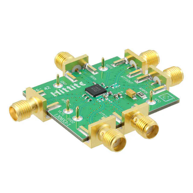
Evaluation PCB
13 - 9
LE
B
SO
List of Materials for Evaluation PCB 130656 [1]
Item
J1 - J5
Description
DC Connector Header
O
Variable gain amplifiers - ANALOG - SMT
13
J6 - J11
PCB Mount SMA RF Connector
C1, C8, C9
10 nF Capacitor, 0402 Pkg
C2, C3, C7
1000 pF Capacitor, 0402 Pkg.
C4, C6
1000 pF Capacitor, 0603 Pkg.
C5
100 pF Capacitor, 0603 Pkg.
C12
2.2 µF Capacitor, CASE A Pkg.
L1
24 nH Inductor 0603 Pkg.
R1, R2
0 Ohm Resistor, 0402 Pkg.
R3
1.8 Ohm Resistor, 1206 Pkg.
U1
HMC972LP5E Variable Gain Amplifier
PCB [2]
130653 Evaluation PCB
The circuit board used in the application should
use RF circuit design techniques. Signal lines should have 50 Ohm impedance while the package
ground leads and exposed paddle should be connected directly to the ground plane similar to that
shown. A sufficient number of via holes should be
used to connect the top and bottom ground planes.
The evaluation circuit board shown is available from
Hittite upon request.
[1] Reference this number when ordering complete evaluation PCB
[2] Circuit Board Material: Rogers 4350
For price,
delivery,
and to placeCorporation:
orders: Analog Devices, Inc.,
For price, delivery, and to place orders, please contact
Hittite
Microwave
One Technology Way, P.O. Box 9106, Norwood, MA 02062-9106
20 Alpha Road, Chelmsford, MA 01824 Phone: Phone:
978-250-3343
978-250-3373
781-329-4700Fax:
• Order
online at www.analog.com
Application Support: Phone: 1-800-ANALOG-D
Order On-line at www.hittite.com
Information furnished by Analog Devices is believed to be accurate and reliable. However, no
responsibility is assumed by Analog Devices for its use, nor for any infringements of patents or other
rights of third parties that may result from its use. Specifications subject to change without notice. No
license is granted by implication or otherwise under any patent or patent rights of Analog Devices.
Trademarks and registered trademarks are the property of their respective owners.
�HMC972LP5E
v00.1210
GaAs MMIC ANALOG VARIABLE
GAIN AMPLIFIER, 0.5 - 6.0 GHz
For price,
delivery,
and to placeCorporation:
orders: Analog Devices, Inc.,
For price, delivery, and to place orders, please contact
Hittite
Microwave
One Technology Way, P.O. Box 9106, Norwood, MA 02062-9106
20 Alpha Road, Chelmsford, MA 01824 Phone: Phone:
978-250-3343
978-250-3373
781-329-4700Fax:
• Order
online at www.analog.com
Application Support: Phone: 1-800-ANALOG-D
Order On-line at www.hittite.com
Information furnished by Analog Devices is believed to be accurate and reliable. However, no
responsibility is assumed by Analog Devices for its use, nor for any infringements of patents or other
rights of third parties that may result from its use. Specifications subject to change without notice. No
license is granted by implication or otherwise under any patent or patent rights of Analog Devices.
Trademarks and registered trademarks are the property of their respective owners.
13
variable gain amplifiers - ANALOG - SMT
O
B
SO
LE
TE
Notes:
13 - 10
�