REVISIONS
LTR
DESCRIPTION
DATE (YR-MO-DA)
APPROVED
REV
SHEET
REV
SHEET
REV STATUS
REV
OF SHEETS
SHEET
PMIC N/A
PREPARED BY
1
2
3
4
5
6
7
8
9
10
Dan Wonnell
STANDARD
MICROCIRCUIT
DRAWING
DEFENSE SUPPLY CENTER COLUMBUS
COLUMBUS, OHIO 43216
CHECKED BY
Raymond Monnin
APPROVED BY
THIS DRAWING IS AVAILABLE
FOR USE BY ALL
DEPARTMENTS AND AGENCIES
OF THEDEPARTMENT OF
DEFENSE
AMSC N/A
Raymond Monnin
DRAWING APPROVAL DATE
98-10-14
REVISION LEVEL
MICROCIRCUIT, DIGITAL-LINEAR, 12-BIT CMOS
DIGITAL TO ANALOG CONVERTER WITH,
OUTPUT AMPLIFIER AND REFERENCE,
MONOLITHIC SILICON
SIZE
CAGE CODE
A
67268
SHEET
DSCC FORM 2233
APR 97
DISTRIBUTION STATEMENT A. Approved for public release; distribution is unlimited.
1 OF
5962-88766
10
5962-E001-99
�1. SCOPE
1.1 Scope. This drawing describes device requirements for MIL-STD-883 compliant, non-JAN class level B microcircuits in
accordance with MIL-PRF-38535, appendix A.
1.2 Part or Identifying Number (PIN). The complete PIN is as shown in the following example:
5962-88766
01
�
�
�
�
�
�
�
�
L
A
Device type
(see 1.2.1)
Case outline
(see 1.2.2)
Lead finish
(see 1.2.3)
�
�
�
�
Drawing number
�
�
�
�
1.2.1 Device type(s). The device type(s) identify the circuit function as follows:
Device type
Generic number
Circuit function
01
AD7245A
12-Bit CMOS DAC with output amplifier
and reference; parallel loading structure
02
AD7248A
12-Bit CMOS DAC with output amplifier
and reference; 8+4 loading structure
1.2.2 Case outline(s). The case outline(s) are as designated in MIL-STD-1835 and as follows:
Outline letter
3
L
R
Descriptive designator
CQCC1-N28
GDIP3-T24 or CDIP4-T24
GDIP1-T20 or CDIP2-T20
Terminals
Package style
28
24
20
Square leadless chip carrier
Dual-in-line
Dual-in-line
1.2.3 Lead finish. The lead finish is as specified in MIL-PRF-38535, appendix A.
1.3 Absolute maximum ratings. 1/
Positive supply voltage (VDD) to AGND....................................
Positive supply voltage (VDD) to DGND ...................................
VDD to VSS ................................................................................
AGND to DGND .......................................................................
Digital input voltage to DGND..................................................
VOUT to AGND ..........................................................................
VOUT to VSS ...............................................................................
VOUT to VDD ..............................................................................
Voltage reference output (REF OUT) to AGND .......................
Power dissipation to +75�C 2/ ................................................
Storage temperature................................................................
Lead temperature (soldering, 10 sec)......................................
-0.3 V dc to +17.0 V dc
-0.3 V dc to +17.0 V dc
-0.3 V dc to +34.0 V dc
-0.3 V dc to VDD
-0.3 V dc to VDD + 0.3 V dc
VSS to VDD
0 V dc to +24.0 V dc
-32 V to 0 V dc
0 v to VDD
450 mW
-65�C to +150�C
+300�C
1/ Stresses above absolute maximum rating may cause permanent damage to the device. Extended operation at the
maximum levels may degrade performance and affect reliability.
2/ Above +75�C, derate at a factor of 6 mW/�C.
STANDARD
MICROCIRCUIT DRAWING
DEFENSE SUPPLY CENTER COLUMBUS
COLUMBUS, OHIO 43216-5000
DSCC FORM 2234
APR 97
SIZE
5962-88766
A
REVISION LEVEL
SHEET
2
�1.4 Recommended operating conditions.
Single supply:
Positive supply voltage (VDD)............................................
Negative supply voltage (VSS)...........................................
AGND = DGND.................................................................
Dual supply:
Positive supply voltage (VDD)............................................
Negative supply voltage (VSS)...........................................
AGND = DGND.................................................................
Load resistance (RL) ................................................................
Load capacitance (CL) .............................................................
REF OUT .................................................................................
Ambient operating temperature range .....................................
+15 V �5%
0V
0V
+12 V to +15 V �5%
-12 V to -15 V �5%
0V
2 k� to GND
100 pF to GND
unloaded
-55 �C to +125�C
2. APPLICABLE DOCUMENTS
2.1 Government specification, standards, and handbooks. The following specification, standards, and handbooks form a
part of this drawing to the extent specified herein. Unless otherwise specified, the issues of these documents are those listed
in the issue of the Department of Defense Index of Specifications and Standards (DoDISS) and supplement thereto, cited in
the solicitation.
SPECIFICATION
DEPARTMENT OF DEFENSE
MIL-PRF-38535 - Integrated Circuits, Manufacturing, General Specification for.
STANDARDS
DEPARTMENT OF DEFENSE
MIL-STD-883 MIL-STD-973 MIL-STD-1835 -
Test Method Standard Microcircuits.
Configuration Management.
Interface Standard For Microcircuit Case Outlines.
HANDBOOKS
DEPARTMENT OF DEFENSE
MIL-HDBK-103 MIL-HDBK-780 -
List of Standard Microcircuit Drawings.
Standard Microcircuit Drawings.
(Unless otherwise indicated, copies of the specification, standards, and handbooks are available from the Standardization
Document Order Desk, 700 Robbins Avenue, Building 4D, Philadelphia, PA 19111-5094.)
2.2 Order of precedence. In the event of a conflict between the text of this drawing and the references cited herein, the text
of this drawing takes precedence. Nothing in this document, however, supersedes applicable laws and regulations unless a
specific exemption has been obtained.
STANDARD
MICROCIRCUIT DRAWING
DEFENSE SUPPLY CENTER COLUMBUS
COLUMBUS, OHIO 43216-5000
DSCC FORM 2234
APR 97
SIZE
5962-88766
A
REVISION LEVEL
SHEET
3
�3. REQUIREMENTS
3.1 Item requirements. The individual item requirements shall be in accordance with MIL-PRF-38535, appendix A for nonJAN class level B devices and as specified herein. Product built to this drawing that is produced by a Qualified Manufacturer
Listing (QML) certified and qualified manufacturer or a manufacturer who has been granted transitional certification to MILPRF-38535 may be processed as QML product in accordance with the manufacturers approved program plan and qualifying
activity approval in accordance with MIL-PRF-38535. This QML flow as documented in the Quality Management (QM) plan
may make modifications to the requirements herein. These modifications shall not affect form, fit, or function of the device.
These modifications shall not affect the PIN as described herein. A "Q" or "QML" certification mark in accordance with MILPRF-38535 is required to identify when the QML flow option is used.
3.2 Design, construction, and physical dimensions. The design, construction, and physical dimensions shall be as
specified in MIL-PRF-38535, appendix A and herein.
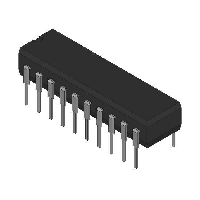
3.2.1 Case outlines. The case outlines shall be in accordance with 1.2.2 herein.
3.2.2 Terminal connections. The terminal connections shall be as specified on figure 1.
3.2.3 Truth tables. The truth tables shall be as specified on figure 2.
3.3 Electrical performance characteristics. Unless otherwise specified herein, the electrical performance characteristics are
as specified in table I and shall apply over the full ambient operating temperature range.
3.4 Electrical test requirements. The electrical test requirements shall be the subgroups specified in table II. The electrical
tests for each subgroup are described in table I.
3.5 Marking. Marking shall be in accordance with MIL-PRF-38535, appendix A. The part shall be marked with the PIN
listed in 1.2 herein. In addition, the manufacturer's PIN may also be marked as listed in MIL-HDBK-103 (see 6.6 herein). For
packages where marking of the entire SMD PIN number is not feasible due to space limitations, the manufacturer has the
option of not marking the "5962-" on the device.
3.6 Certificate of compliance. A certificate of compliance shall be required from a manufacturer in order to be listed as an
approved source of supply in MIL-HDBK-103 (see 6.6 herein). The certificate of compliance submitted to DSCC-VA prior to
listing as an approved source of supply shall affirm that the manufacturer's product meets the requirements of MIL-PRF-38535,
appendix A and the requirements herein.
3.7 Certificate of conformance. A certificate of conformance as required in MIL-PRF-38535, appendix A shall be provided with
each lot of microcircuits delivered to this drawing.
3.8 Notification of change. Notification of change to DSCC-VA shall be required in accordance with MIL-PRF-38535,
appendix A.
3.9 Verification and review. DSCC, DSCC's agent, and the acquiring activity retain the option to review the manufacturer's
facility and applicable required documentation. Offshore documentation shall be made available onshore at the option of the
reviewer.
STANDARD
MICROCIRCUIT DRAWING
DEFENSE SUPPLY CENTER COLUMBUS
COLUMBUS, OHIO 43216-5000
DSCC FORM 2234
APR 97
SIZE
5962-88766
A
REVISION LEVEL
SHEET
4
�TABLE I. Electrical performance characteristics.
Test
Symbol
Conditions 1/
-55�C � TA �+125�C
unless otherwise specified
Group A
subgroups
Device
type
1, 2, 3
All
VDD = +11.4 V to +15.75 V
VSS = -11.4 V to -15.75 V
1, 2, 3
All
Limits
Min
Resolution
RES
Relative accuracy
RA
Unit
Max
12
Bits
-1
+1
LSB
Differential nonlinearity
DNL
Guaranteed monotonic
1, 2, 3
All
-1
+1
LSB
Unipolar offset error
UOE
VSS = 0 V or
-11.4 V to -15.75 V
1, 2, 3
All
-5
+5
LSB
1, 2, 3
All
-2
+2
LSB
1
All
-.2
+.2
%FSR
-.6
+.6
DAC gain error 2/
Full scale output voltage
GE
V OUTE
VDD = +15 V
error 3/
�Full
2, 3
scale/�VDD
�Full
scale/�VSS
Reference output
VREFOUT
VDD = +10.8 V to +16.5 V
1
All
-.06
+.06
%FSR/V
VSS = -10.8 V to -16.5 V
1
All
-.01
-.01
%FSR/V
4.99
5.01
V
2
mV/V
+1.0
mV
VDD = +15 V, VSS = -15 V
1
All
�Reference/�VDD
VDD = +10.8 V to +16.5 V
1
All
Reference load sensitivity
Reference load current
change (0-100 �A). Not
including ROFS current.
1, 2, 3
All
-1.0
1, 2, 3
All
2.4
1, 2, 3
All
1, 2, 3
All
4
5/
All
1, 2, 3
All
1, 2, 3
All
Digital input high voltage
VINH
Digital input low voltage
VINL
Digital input current for
data and control inputs 4/
Digital input capacitance
Output range resistors
IIN
VIN = 0 or VDD
CIN
see 4.3.1b
ROUT
Output ranges 6/
Pin strappable
Minimum load resistance
2 k to GND
Power supply current
IDD
Output unloaded
1, 2, 3
All
7, 8
All
4
5/
All
4, 5, 6
5/
All
-10
15
Output voltage settling
positive and negative
full scale change 7/
Output voltage slew rate
0.8
V
+10
�A
8
pF
30
�
V
0
5
0
10
-5
+5
12
ISS
Functional tests
V
mA
5
see 4.3.1c
tSL
To �0.5 LSB, RL = 2 k�,
see 4.3.1b
SR
see 4.3.1b
10
�s
1.5
V/�s
See footnotes at end of table.
STANDARD
MICROCIRCUIT DRAWING
DEFENSE SUPPLY CENTER COLUMBUS
COLUMBUS, OHIO 43216-5000
DSCC FORM 2234
APR 97
SIZE
5962-88766
A
REVISION LEVEL
SHEET
5
�TABLE I. Electrical performance characteristics - continued.
Test
Symbol
Conditions 1/
-55�C � TA �+125�C
unless otherwise specified
Group A
subgroups
Device
type
Limits
Unit
Chip select pulse width
t1
9, 10, 11
All
Min
100
Max
Write pulse width
t2
9, 10, 11
All
100
ns
Chip select to write setup
t3
9, 10, 11
All
0
ns
Chip select to write hold
t4
9, 10, 11
All
0
ns
Data valid to write setup
time
Data valid to write hold
time
Load DAC pulse width
t5
9, 10, 11
All
80
ns
t6
9, 10, 11
All
10
ns
t7
9, 10, 11
All
100
ns
Clear pulse width
t8
9, 10, 11
01
100
ns
ns
1/ Dual supply: VDD = 11.4 V to 15.75 V, VSS = 0 V or -11.4 V to -15.75 V, AGND = DGND = 0 V, RL = 2 k� to GND,
CL = 100 pF to GND. REF unloaded, unless otherwise stated.
2/ This error is calculated with respect to the reference voltage and is measured after the offset error has been allowed for.
3/ This error is calculated with respect to an ideal 4.9988 V (on the 5 V range) or 9.9976 V (on the 10 V range). Typical full
scale temperature coefficient is �30 ppm of FSSR/�C.
4/ Control inputs are CS, WR, LADC and CLR for device 01 and CSMSB, CSLSB, WR and LDAC for device 02.
5/ Subgroups 4, 5 and 6 shall be measured only for initial test, or after process or design changes which may affect the
parameter in those subgroups.
6/ 0 to +10 applies to VDD = +15 V �5% only, and VSS = -15 V �5%.
7/ For positive full scale change, DAC register loaded all 0’s to all 1’s. For negative full scale change, DAC register loaded all
1’s to all 0’s.
STANDARD
MICROCIRCUIT DRAWING
DEFENSE SUPPLY CENTER COLUMBUS
COLUMBUS, OHIO 43216-5000
DSCC FORM 2234
APR 97
SIZE
5962-88766
A
REVISION LEVEL
SHEET
6
�Device type
01
Case outlines
02
3
Terminal number
L
R
Terminal symbol
1
NC
VSS
VSS
2
VSS
ROFS
ROFS
3
ROFS
REF OUT
REF OUT
4
REF OUT
AGND
AGND
5
AGND
DB11
(MSB) DB7
6
DB11
DB10
DB6
7
DB10
DB9
DB5
8
NC
DB8
DB4
9
DB9
DB7
DB3
10
DB8
DB6
DGND
11
DB7
DB5
DB2
12
DB6
DGND
DB1
13
DB5
DB4
(LSB) DB0
14
DGND
DB3
CSMSB
15
NC
DB2
CSLSB
16
DB4
DB1
WR
17
DB3
DB0
LDAC
18
DB2
CS
VDD
19
DB1
WR
RFB
20
DB0
LDAC
VOUT
21
CS
CLR
22
NC
VDD
23
WR
RFB
24
LDAC
VOUT
25
CLR
26
VDD
27
RFB
28
VOUT
FIGURE 1. Terminal connections.
STANDARD
MICROCIRCUIT DRAWING
DEFENSE SUPPLY CENTER COLUMBUS
COLUMBUS, OHIO 43216-5000
DSCC FORM 2234
APR 97
SIZE
5962-88766
A
REVISION LEVEL
SHEET
7
�Device type 01
CLR
H
H
H
H
H
H
H
L
LDAC
L
H
H
H
H
L
WR
L
H
X
L
��
��
X
H
H
H
X
H
��
L
L
��
H = High state
CS
L
X
H
L
L
H
H
X
H
L
Function
Both latches are transparent
Both latches are latched
Both latches are latched
Input latches are transparent
Input latches are latched
DAC latches are transparent
DAC latches are latched
DAC latches loaded with all 0’s
DAC latches loaded with all 0’s and
output remains at 0 V 0r -5 V
Both latches are transparent and
output follows input data
L = Low state
X = Don’t care
Device type 02
CSLSB
L
L
��
H
H
H
H
H
H
H
CSMSB
H
H
H
L
L
WR
L
��
H
H
L
L
H
H
L
H
H
��
L
L
��
LDAC
H
H
H
H
H
H
L
��
L
H
H = High state
Funtion
Loads LS byte into input latch
Latches LS byte into input latch
Latches LS byte into input latch
Loads MS nibble into input latch
Latches MS nibble into input latch
Latches MS nibble into input latch
Loads input latch into DAC latch
Latches input latch into DAC latch
Loads MS nibble into input latch and
Loads input latch into DAC latch
No data transfer operation
L = Low state
X = Don’t care
FIGURE 2. Truth tables.
STANDARD
MICROCIRCUIT DRAWING
DEFENSE SUPPLY CENTER COLUMBUS
COLUMBUS, OHIO 43216-5000
DSCC FORM 2234
APR 97
SIZE
5962-88766
A
REVISION LEVEL
SHEET
8
�4. QUALITY ASSURANCE PROVISIONS
4.1 Sampling and inspection. Sampling and inspection procedures shall be in accordance with MIL-PRF-38535,
appendix A.
4.2 Screening. Screening shall be in accordance with method 5004 of MIL-STD-883, and shall be conducted on all devices
prior to quality conformance inspection. The following additional criteria shall apply:
a.
Burn-in test, method 1015 of MIL-STD-883.
(1) Test condition A, B, C, or D. The test circuit shall be maintained by the manufacturer under document revision
level control and shall be made available to the preparing or acquiring activity upon request. The test circuit shall
specify the inputs, outputs, biases, and power dissipation, as applicable, in accordance with the intent specified in
test method 1015 of MIL-STD-883.
(2) TA = +125�C, minimum.
b.
Interim and final electrical test parameters shall be as specified in table II herein, except interim electrical parameter
tests prior to burn-in are optional at the discretion of the manufacturer.
TABLE II. Electrical test requirements.
MIL-STD-883 test requirements
Subgroups
(in accordance with
MIL-STD-883, method 5005,
table I)
Interim electrical parameters
(method 5004)
1
Final electrical test parameters
(method 5004)
1,2,3
Group A test requirements
(method 5005)
1, 2, 3, 9, 10, 11
Groups C and D end-point
electrical parameters
(method 5005)
1
* PDA applies to subgroup 1.
4.3 Quality conformance inspection. Quality conformance inspection shall be in accordance with method 5005 of
MIL-STD-883 including groups A, B, C, and D inspections. The following additional criteria shall apply.
4.3.1 Group A inspection.
a.
Tests shall be as specified in table II herein.
b.
Subgroup 4, 5 and 6 shall be measured only for the initial test and after process or design changes which may affect
the specified parameters in those subgroups.
c.
Subgroups 7 and 8 shall include verification of the truth table.
STANDARD
MICROCIRCUIT DRAWING
DEFENSE SUPPLY CENTER COLUMBUS
COLUMBUS, OHIO 43216-5000
DSCC FORM 2234
APR 97
SIZE
5962-88766
A
REVISION LEVEL
SHEET
9
�4.3.2 Groups C and D inspections.
a.
End-point electrical parameters shall be as specified in table II herein.
b.
Steady-state life test conditions, method 1005 of MIL-STD-883.
(1)
Test condition A, B, C, or D. The test circuit shall be maintained by the manufacturer under document revision
level control and shall be made available to the preparing or acquiring activity upon request. The test circuit
shall specify the inputs, outputs, biases, and power dissipation, as applicable, in accordance with the intent
specified in test method 1005 of MIL-STD-883.
(2)
TA = +125�C, minimum.
(3)
Test duration: 1,000 hours, except as permitted by method 1005 of MIL-STD-883.
5. PACKAGING
5.1 Packaging requirements. The requirements for packaging shall be in accordance with MIL-PRF-38535, appendix A.
6. NOTES
6.1 Intended use. Microcircuits conforming to this drawing are intended for use for Government microcircuit applications
(original equipment), design applications, and logistics purposes.
6.2 Replaceability. Microcircuits covered by this drawing will replace the same generic device covered by a
contractor-prepared specification or drawing.
6.3 Configuration control of SMD's. All proposed changes to existing SMD's will be coordinated with the users of record for
the individual documents. This coordination will be accomplished in accordance with MIL-STD-973 using DD Form 1692,
Engineering Change Proposal.
6.4 Record of users. Military and industrial users shall inform Defense Supply Center Columbus when a system application
requires configuration control and the applicable SMD. DSCC will maintain a record of users and this list will be used for
coordination and distribution of changes to the drawings. Users of drawings covering microelectronics devices (FSC 5962)
should contact DSCC-VA, telephone (614) 692-0525.
6.5 Comments. Comments on this drawing should be directed to DSCC-VA, Columbus, Ohio 43216-5000, or telephone
(614) 692-0674.
6.6 Approved sources of supply. Approved sources of supply are listed in MIL-HDBK-103. The vendors listed in MILHDBK-103 have agreed to this drawing and a certificate of compliance (see 3.6 herein) has been submitted to and accepted
by DSCC-VA.
STANDARD
MICROCIRCUIT DRAWING
DEFENSE SUPPLY CENTER COLUMBUS
COLUMBUS, OHIO 43216-5000
DSCC FORM 2234
APR 97
SIZE
5962-88766
A
REVISION LEVEL
SHEET
10
�STANDARD MICROCIRCUIT DRAWING BULLETIN
DATE: 98-10-14
Approved sources of supply for SMD 5962-88766 are listed below for immediate acquisition information only and
shall be added to MIL-HDBK-103 and QML-38535 during the next revision. MIL-HDBK-103 and QML-38535 will be
revised to include the addition or deletion of sources. The vendors listed below have agreed to this drawing and a
certificate of compliance has been submitted to and accepted by DSCC-VA. This bulletin is superseded by the next
dated revision of MIL-HDBK-103 and QML-38535.
Standard
microcircuit drawing
PIN 1/
Vendor
CAGE
number
Vendor
similar
PIN 2/
5962-88766013A
24355
AD7245ATE/883B
5962-8876601LA
24355
AD7245ATQ/883B
5962-8876602RA
24355
AD7248ATQ/883B
1/ The lead finish shown for each PIN representing
a hermetic package is the most readily available
from the manufacturer listed for that part. If the
desired lead finish is not listed contact the vendor
to determine its availability.
2/ Caution. Do not use this number for item
acquisition. Items acquired to this number may not
satisfy the performance requirements of this drawing.
Vendor CAGE
number
24355
Vendor name
and address
Analog Devices
RT 1 Industrial Park
P.O. Box 9106
Norwood MA 02062
Point of contact:
Bay F-1
Raheen IND. Estate
Limerick, Ireland
The information contained herein is disseminated for convenience only and the
Government assumes no liability whatsoever for any inaccuracies in the
information bulletin.
�