REVISIONS
LTR
DESCRIPTION
A
DATE (YR-MO-DA)
APPROVED
01-07-13
Raymond Monnin
Drawing updated to reflect current requirements. - lgt
THE ORIGINAL FIRST SHEET OF THIS DRAWING HAS BEEN REPLACED.
REV
SHEET
REV
A
A
A
A
A
A
A
A
SHEET
15
16
17
18
19
20
21
22
REV STATUS
REV
A
A
A
A
A
A
A
A
A
A
A
A
A
A
OF SHEETS
SHEET
1
2
3
4
5
6
7
8
9
10
11
12
13
14
PMIC N/A
PREPARED BY
Joseph A. Kirby
STANDARD
MICROCIRCUIT
DRAWING
THIS DRAWING IS AVAILABLE
FOR USE BY ALL
DEPARTMENTS
AND AGENCIES OF THE
DEPARTMENT OF DEFENSE
AMSC N/A
DEFENSE SUPPLY CENTER COLUMBUS
COLUMBUS, OHIO 43216
http://www.dscc.dla.mil
CHECKED BY
Charles E. Besore
APPROVED BY
Michael Frye
MICROCIRCUIT, LINEAR, 8-BIT ANALOG I/O
SYSTEM, MONOLITHIC SILICON
DRAWING APPROVAL DATE
06 May 1991
REVISION LEVEL
A
SIZE
CAGE CODE
A
67268
SHEET
DSCC FORM 2233
APR 97
DISTRIBUTION STATEMENT A. Approved for public release; distribution is unlimited.
1 OF
5962-89629
22
5962-E488-01
�1. SCOPE
1.1 Scope. This drawing describes device requirements for MIL-STD-883 compliant, non-JAN class level B microcircuits in
accordance with MIL-PRF-38535, appendix A.
1.2 Part or Identifying Number (PIN). The complete PIN is as shown in the following example:
5962-89629
01
L
X
Drawing number
Device type
(see 1.2.1)
Case outline
(see 1.2.2)
Lead finish
(see 1.2.3)
1.2.1 Device type(s). The device type(s) identify the circuit function as follows:
Device type
Generic number
01
02
AD7569S
AD7569T
Circuit function
Relative Accuracy
�1 LSB for DAC and ADC
�1/2 LSB for DAC and ADC
8-bit analog I/O system
8-bit analog I/O system
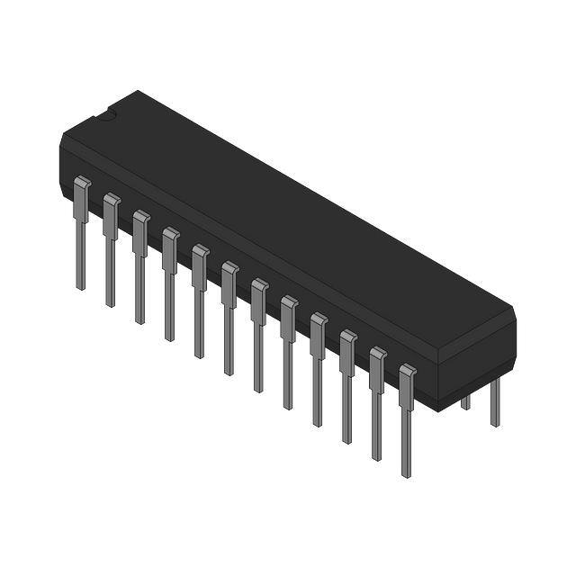
1.2.2 Case outline(s). The case outline(s) are as designated in MIL-STD-1835 and as follows:
Outline letter
L
3
Descriptive designator
Terminals
GDIP3-T24 or CDIP4-T24
CQCC1-N28
24
28
Package style
Dual-in-line
Square leadless chip carrier
1.2.3 Lead finish. The lead finish is as specified in MIL-PRF-38535, appendix A.
1.3 Absolute maximum ratings.
Supply voltage (VDD) to AGNDDAC or AGNDADC .................................... -0.3 V dc to +7.0 V dc
Supply voltage (VDD) to DGND ............................................................. -0.3 V dc to +7.0 V dc
VDD to VSS ............................................................................................. -0.3 V dc to +14 V dc
AGNDDAC or AGNDADC to DGND .......................................................... -0.3 V dc to VDD +0.3 V dc
AGNDDAC or AGNDADC ......................................................................... �5.0 V dc
Logic voltage to DGND......................................................................... -0.3 V dc to VDD +0.3 V dc
CLK input voltage to DGND.................................................................. -0.3 V dc to VDD +0.3 V dc
Output voltage to AGNDDAC 1/............................................................. VSS -0.3 V dc to VDD +0.3 V dc
Input voltage to AGNDADC .................................................................... VSS -0.3 V dc to VDD +0.3 V dc
Storage temperature range .................................................................. -65�C to +150�C
Lead temperature (soldering, 10 seconds)........................................... +300�C
Power dissipation (PD).......................................................................... 450 mW 2/
Thermal resistance, junction to case (�JC) ........................................... See MIL-STD-1835
Thermal resistance, junction to ambient (�JA) ...................................... 120�C/W
Junction temperature (TJ)..................................................................... +150�C
1.4 Recommended operating conditions.
Supply voltage to ground (VSS)............................................................ -4.75 V dc to –5.25 V dc
Supply voltage to ground (V DD) ........................................................... +4.75 V dc to +5.25 V dc
Ambient operating temperature range (T A) .......................................... -55�C to +125�C
1/
2/
Output may be shorted to any voltage in the range VSS to VDD provided that the power dissipation of the package is not
exceeded.
Derate above TA = +75�C at 6.0 mW/�C.
STANDARD
MICROCIRCUIT DRAWING
DEFENSE SUPPLY CENTER COLUMBUS
COLUMBUS, OHIO 43216-5000
DSCC FORM 2234
APR 97
SIZE
5962-89629
A
REVISION LEVEL
A
SHEET
2
�2. APPLICABLE DOCUMENTS
2.1 Government specification, standards, and handbooks. The following specification, standards, and handbooks form a
part of this drawing to the extent specified herein. Unless otherwise specified, the issues of these documents are those listed
in the issue of the Department of Defense Index of Specifications and Standards (DoDISS) and supplement thereto, cited in
the solicitation.
SPECIFICATION
DEPARTMENT OF DEFENSE
MIL-PRF-38535 -- Integrated Circuits, Manufacturing, General Specification for.
STANDARDS
DEPARTMENT OF DEFENSE
MIL-STD-883 MIL-STD-1835 -
Test Method Standard Microcircuits.
Interface Standard Electronic Component Case Outlines.
HANDBOOKS
DEPARTMENT OF DEFENSE
MIL-HDBK-103 -- List of Standard Microcircuit Drawings.
MIL-HDBK-780 - Standard Microcircuit Drawings.
(Unless otherwise indicated, copies of the specification, standards, and handbooks are available from the Standardization
Document Order Desk, 700 Robbins Avenue, Building 4D, Philadelphia, PA 19111-5094.)
2.2 Order of precedence. In the event of a conflict between the text of this drawing and the references cited herein, the text
of this drawing takes precedence. Nothing in this document, however, supersedes applicable laws and regulations unless a
specific exemption has been obtained.
3. REQUIREMENTS
3.1 Item requirements. The individual item requirements shall be in accordance with MIL-PRF-38535, appendix A for nonJAN class level B devices and as specified herein. Product built to this drawing that is produced by a Qualified Manufacturer
Listing (QML) certified and qualified manufacturer or a manufacturer who has been granted transitional certification to MILPRF-38535 may be processed as QML product in accordance with the manufacturers approved program plan and qualifying
activity approval in accordance with MIL-PRF-38535. This QML flow as documented in the Quality Management (QM) plan
may make modifications to the requirements herein. These modifications shall not affect form, fit, or function of the device.
These modifications shall not affect the PIN as described herein. A "Q" or "QML" certification mark in accordance with MILPRF-38535 is required to identify when the QML flow option is used.
3.2 Design, construction, and physical dimensions. The design, construction, and physical dimensions shall be as
specified in MIL-PRF-38535, appendix A and herein.
3.2.1 Terminal connections. The terminal connections shall be as specified on figure 1.
3.2.2 Pin descriptions. The pin descriptions shall be as specified on figure 2.
3.2.3 Truth table. The truth table shall be as specified on figure 3.
3.2.4 Input/output voltage ranges and unipolar/bipolar code tables. The input/output voltage ranges and unipolar/bipolar
code tables shall be as specified on figure 4.
3.2.5 Logic diagram. The logic diagram shall be as specified on figure 5.
3.2.6 Load circuits. The load circuits shall be as specified on figure 6.
STANDARD
MICROCIRCUIT DRAWING
DEFENSE SUPPLY CENTER COLUMBUS
COLUMBUS, OHIO 43216-5000
DSCC FORM 2234
APR 97
SIZE
5962-89629
A
REVISION LEVEL
A
SHEET
3
�3.2.7 Write cycle timing waveforms. The write cycle timing waveforms shall be as specified on figure 7.
3.2.8 ADC mode 1 interface timing waveforms. The ADC mode 1 interface timing waveforms shall be as specified on figure
8.
3.2.9 ADC mode 2 interface timing waveforms. The ADC mode 2 interface timing waveforms shall be as specified on figure
9.
3.2.10 Equivalent input voltage circuit. The equivalent input voltage circuit shall be as specified on figure 10.
3.2.11 Case outline(s). The case outline(s) shall be in accordance with 1.2.2 herein.
3.3 Electrical performance characteristics. Unless otherwise specified herein, the electrical performance characteristics are
as specified in table I and shall apply over the full ambient operating temperature range.
3.4 Electrical test requirements. The electrical test requirements shall be the subgroups specified in table II. The electrical
tests for each subgroup are described in table I.
3.5 Marking. Marking shall be in accordance with MIL-PRF-38535, appendix A. The part shall be marked with the PIN
listed in 1.2 herein. In addition, the manufacturer's PIN may also be marked as listed in MIL-HDBK-103 (see 6.6 herein). For
packages where marking of the entire SMD PIN number is not feasible due to space limitations, the manufacturer has the
option of not marking the "5962-" on the device.
3.5.1 Certification/compliance mark. A compliance indicator “C” shall be marked on all non-JAN devices built in compliance
to MIL-PRF-38535, appendix A. The compliance indicator “C” shall be replaced with a "Q" or "QML" certification mark in
accordance with MIL-PRF-38535 to identify when the QML flow option is used.
3.6 Certificate of compliance. A certificate of compliance shall be required from a manufacturer in order to be listed as an
approved source of supply in MIL-HDBK-103 (see 6.6 herein). The certificate of compliance submitted to DSCC-VA prior to
listing as an approved source of supply shall affirm that the manufacturer's product meets the requirements of MIL-PRF38535, appendix A and the requirements herein.
3.7 Certificate of conformance. A certificate of conformance as required in MIL-PRF-38535, appendix A shall be provided
with each lot of microcircuits delivered to this drawing.
3.8 Notification of change. Notification of change to DSCC-VA shall be required in accordance with MIL-PRF-38535,
appendix A.
3.9 Verification and review. DSCC, DSCC's agent, and the acquiring activity retain the option to review the manufacturer's
facility and applicable required documentation. Offshore documentation shall be made available onshore at the option of the
reviewer.
4. QUALITY ASSURANCE PROVISIONS
4.1 Sampling and inspection. Sampling and inspection procedures shall be in accordance with MIL-PRF-38535,
appendix A.
4.2 Screening. Screening shall be in accordance with method 5004 of MIL-STD-883, and shall be conducted on all devices
prior to quality conformance inspection. The following additional criteria shall apply:
a.
Burn-in test, method 1015 of MIL-STD-883.
(1) Test condition A, B, C, or D. The test circuit shall be maintained by the manufacturer under document revision level
control and shall be made available to the preparing or acquiring activity upon request. The test circuit shall
specify the inputs, outputs, biases, and power dissipation, as applicable, in accordance with the intent specified in
test method 1015 of MIL-STD-883.
(2) TA = +125�C, minimum.
b.
Interim and final electrical test parameters shall be as specified in table II herein, except interim electrical parameter
tests prior to burn-in are optional at the discretion of the manufacturer.
STANDARD
MICROCIRCUIT DRAWING
DEFENSE SUPPLY CENTER COLUMBUS
COLUMBUS, OHIO 43216-5000
DSCC FORM 2234
APR 97
SIZE
5962-89629
A
REVISION LEVEL
A
SHEET
4
�TABLE I. Electrical performance characteristics.
Test
Symbol
Conditions 1/
CL = 100 pF to AGNDDAC
RL = 2.0 k�
-55�C � TA �+125�C
unless otherwise specified
Group A
subgroups
Device
type
Limits
Min
DAC specifications
Relative accuracy
INL
01
1, 2, 3
02
1
DNL
Guaranteed monotonic
01
1, 2, 3
02
1
2, 3, 12
Unipolar offset error
DAC data is all zeros,
VSS = 0 V
ALL
1
01
2, 3
02
2, 3
1, 12
Bipolar zero offset
error
DAC data is all zeros,
VSS = -5.0 V
ALL
1
01
2, 3
02
2, 3
Max
�1.0
�1.0
�1/2
�1.0
2, 3, 12
Differential
nonlinearity
Unit
LSB
LSB
�1.0
�3/4
�2.0
LSB
�2.5
�2.0
�1.5
�2.0
LSB
LSB
12
�2.5
�2.0
�1.5
�2.0
�4.0
�3.0
�1.0
ALL
1
0.5
LSB
ALL
1
0.5
LSB
VIL
ALL
1, 2, 3
0.8
V
VIH
ALL
1, 2, 3
1, 12
Full-scale error
VDD = 5.0 V
2/
TA = +25�C,
�Full scale
�VDD
ALL
1
01
2, 3
02
2, 3
VOUT = 2.5 V,
� VDD = �5%
TA = +25�C,
�Full scale
�VSS
VOUT = -2.5 V,
� VSS = �5%
Digital input voltage
low level
Digital input voltage
high level
Input leakage current
Positive power supply
current
2.4
V
IIL
VIN = 0 to VDD
ALL
1, 2, 3
10
�A
IDD
VOUT = VIN = 2.5 V,
Logic units = 2.4 V,
CLK = 0.8 V, output
unloaded
ALL
1, 2, 3
13
mA
See footnotes at end of table.
STANDARD
MICROCIRCUIT DRAWING
DEFENSE SUPPLY CENTER COLUMBUS
COLUMBUS, OHIO 43216-5000
DSCC FORM 2234
APR 97
SIZE
5962-89629
A
REVISION LEVEL
A
SHEET
5
�TABLE I. Electrical performance characteristics - Continued.
Test
Symbol
Conditions 1/
CL = 100 pF to AGNDDAC
RL = 2.0 k�
-55�C � TA �+125�C
unless otherwise specified
Group A
subgroups
Device
type
Limits
Min
DAC specifications - Continued
Negative power
ISS
supply current
(dual supply)
Input capacitance
Signal-to-noise ratio
CIN
SNR
THD
Functional test
WR pulse width
t1
ALL
1, 2, 3
4.0
mA
See 4.3.1d
ALL
4
10
pF
01
4, 5, 6
VOUT = 20 kHz full
scale sine wave with
fSAMPLING = 400 kHz
44
VOUT = 20 kHz full
scale sine wave with
fSAMPLING = 400 kHz
ALL
4, 5, 6
See 4.3.1b
ALL
7, 8
See figure 7
3/
ALL
dB
46
48
9
80
10, 11
90
CS , A B to WR
setup time
t2
ALL
9, 10, 11
0
CS , A B to WR
hold time
t3
ALL
9, 10, 11
0
Data valid to WR
setup time
t4
ALL
9
60
10, 11
80
t5
ALL
9, 10, 11
10
Data valid to WR
hold time
Max
VOUT = VIN = -2.5 V,
Logic units = 2.4 V,
CLK = 0.8 V, output
unloaded
02
Total harmonic
distortion
Unit
dB
ns
See footnotes at end of table.
STANDARD
MICROCIRCUIT DRAWING
DEFENSE SUPPLY CENTER COLUMBUS
COLUMBUS, OHIO 43216-5000
DSCC FORM 2234
APR 97
SIZE
5962-89629
A
REVISION LEVEL
A
SHEET
6
�TABLE I. Electrical performance characteristics - Continued.
Test
Symbol
Conditions 1/
fCLK = 5.0 MHz
-55�C � TA �+125�C
unless otherwise specified
Group A
subgroups
Device
type
Limits
Min
ADC specifications
Relative accuracy
INL
01
1, 2, 3
02
2, 3, 12
DNL
No missing codes
01
1, 2, 3
02
2, 3, 12
VSS = 0 V
ALL
1
01
2, 3
02
2, 3
1, 12
Bipolar zero offset
error
VSS = -5.0 V
ALL
1
01
2, 3
02
2, 3
LSB
LSB
�3/4
�1
�2.0
�3.0
�2.5
�1.5
�3.0
1
Unipolar offset error
Max
�1
�1/2
�1
�1
1
Differential
nonlinearity
Unit
LSB
LSB
�1.25 V range
�4.0
�3.5
�2.5
12
Full scale error
VDD = 5.0 V
�Full scale
�VDD
VIN = 2.5 V,
�Full scale
�VSS
VIN = -2.5 V,
2/
ALL
1
-4.0
0
LSB
2, 3
-7.5
2.0
ALL
1
0.5
LSB
ALL
1
0.5
LSB
0.8
V
� VDD = �5%
� VSS = �5%
Input voltage low level
VIL
ALL
1, 2, 3
Input voltage high
level
Analog input current
VIH
ALL
1, 2, 3
IIN
See figure 10
ALL
1, 2, 3
�300
Input leakage current
IIL
CS , RD , ST , Range,
ALL
1, 2, 3
10
�A
�A
2.4
V
RESET
CLK input current low
level
CLK input current
high level
IINL
VIN = 0 V
ALL
1, 2, 3
-1.6
mA
IINH
VIN = VDD
ALL
1, 2, 3
40
�A
See footnotes at end of table.
STANDARD
MICROCIRCUIT DRAWING
DEFENSE SUPPLY CENTER COLUMBUS
COLUMBUS, OHIO 43216-5000
DSCC FORM 2234
APR 97
SIZE
5962-89629
A
REVISION LEVEL
A
SHEET
7
�TABLE I. Electrical performance characteristics - Continued.
Test
Symbol
Conditions 1/
fCLK = 5.0 MHz
-55�C � TA �+125�C
unless otherwise specified
Group A
subgroups
Device
type
Limits
Min
ADC specifications - Continued
Output voltage low
VOL
level
Output voltage high
VOH
level
Floating state leakage
IOUT
current
Positive power supply
IDD
current
Negative power
supply current
(dual supplies)
Input capacitance
Floating state output
capacitance
Signal-to-noise ratio
Max
ISINK = 1.6 mA
ALL
1, 2, 3
0.4
ISOURCE = 200 �A
ALL
1, 2, 3
V
ALL
1, 2, 3
�10
�A
VOUT = VIN = 2.5 V,
Logic units = 2.4 V,
CLK = 0.8 V, output
unloaded
ALL
1, 2, 3
13
mA
ISS
VOUT = VIN = -2.5 V,
Logic units = 2.4 V,
CLK = 0.8 V, output
unloaded
ALL
1, 2, 3
4.0
mA
4.0
V
CIN
See 4.3.1d
ALL
4
10
pF
COUT
See 4.3.1d
ALL
4
10
pF
SNR
VIN = 100 kHz full
scale sine wave with
fSAMPLING = 400 kHz 4/
01
4, 5, 6
44
02
Total harmonic
distortion
Unit
THD
Conversion time with
external clock
Conversion time with
internal clock
Functional test
dB
45
VIN = 100 kHz full
scale sine wave with
fSAMPLING = 400 kHz 4/
ALL
4, 5, 6
48
dB
fCLK = 5.0 MHz
ALL
9, 10, 11
2.0
�s
ALL
9, 10, 11
2.6
�s
See 4.3.1b
See figure 8
3/
1.6
ALL
7, 8
ALL
9, 10, 11
9
110
50
ns
ST pulse width
t6
ST to BUSY delay
t7
ALL
10, 11
150
BUSY to INT delay
t8
ALL
9
20
BUSY to CS delay
t9
ALL
9, 10, 11
0
CS to RD setup time
t10
ALL
9, 10, 11
0
10, 11
30
See footnotes at end of table.
STANDARD
MICROCIRCUIT DRAWING
DEFENSE SUPPLY CENTER COLUMBUS
COLUMBUS, OHIO 43216-5000
DSCC FORM 2234
APR 97
SIZE
5962-89629
A
REVISION LEVEL
A
SHEET
8
�TABLE I. Electrical performance characteristics - Continued.
Test
Symbol
Conditions 1/
CL = 100 pF to AGNDDAC
RL = 2.0 k�
-55�C � TA �+125�C
unless otherwise specified
Group A
subgroups
Device
type
Limits
Min
ADC specifications - Continued
t11
RD pulse width
determined by t13
CS to RD hold time
Data access time
after RD
RD to INT delay
RD to BUSY delay
Data valid after
BUSY
3/ 5/
t12
t13
Data access time
after RD
Bus relinquish time
5/ 7
after RD
See figure 8
t14
t15
See figure 8
CL = 20 pF
3/
6/
10, 11
90
ns
9, 10, 11
0
9
60
10, 11
90
9
95
10, 11
135
9
10
60
10, 11
10
85
6/
ALL
See figure 8
3/
7/
ALL
3/
60
ALL
3/
See figure 8
9
Max
ALL
See figure 8
CL = 100 pF
ALL
ALL
t16
t17
ALL
Unit
See figure 9
CL = 20 pF
3/
6/
ALL
See figure 9
CL = 100 pF
3/
6/
ALL
9
65
10, 11
85
9
120
10, 11
160
9
60
10, 11
90
9
90
10, 11
135
ns
See footnotes at end of table.
STANDARD
MICROCIRCUIT DRAWING
DEFENSE SUPPLY CENTER COLUMBUS
COLUMBUS, OHIO 43216-5000
DSCC FORM 2234
APR 97
SIZE
5962-89629
A
REVISION LEVEL
A
SHEET
9
�TABLE I. Electrical performance characteristics - Continued.
1/
Unless otherwise specified, VDD = 5.0 �5%, VSS = RANGE = AGNDADC = DGND = 0 V; specifications apply for all
output ranges including bipolar ranges with dual supply operation.
2/
Includes internal voltage reference error and is calculated after offset error has been adjusted out.
For DAC specifications :
a) Ideal unipolar full scale voltage is (FS – 1 LSB).
b) Ideal bipolar positive full scale voltage is (FS/2 – 1 LSB).
c) Ideal unipolar negative full scale voltage is (-FS/2).
For DAC specifications :
a) Ideal unipolar last code transition occurs at (FS – 3/2 LSB).
b) Ideal bipolar last code transition occurs at (FS/2 – 3/2 LSB).
3/
All input control signals are specified with tR = tF = 5.0 ns (10% to 90% of +5.0 V) and timed from a voltage level of
1.6 V. ADC is sample tested in mode 1 only.
4/
Exact frequencies are 101 kHz and 384 kHz to avoid harmonics coinciding with sampling frequency.
5/
Tested initially and after process and design changes only.
6/
t13 and t17 are measured with the load circuits on figure 6 and defined as the time required for an output to cross
either 0.8 V or 2.4 V.
7/
t14 is defined as the time required for the data line to change 0.5 V when loaded with circuit on figure 6.
STANDARD
MICROCIRCUIT DRAWING
DEFENSE SUPPLY CENTER COLUMBUS
COLUMBUS, OHIO 43216-5000
DSCC FORM 2234
APR 97
SIZE
5962-89629
A
REVISION LEVEL
A
SHEET
10
�Device type
01 and 02
01
Case outline
L
3
Terminal Number
Terminal symbol
1
2
3
4
5
NC
AGNDDAC
VOUT
VSS
RANGE
AGNDDAC
VOUT
VSS
RANGE
6
RESET
DB7
7
8
9
10
11
12
13
DB6
DB5
DB4
DB3
DB2
DGND
DB1
14
15
16
DB0
17
18
RD
ST
DB0
19
BUSY
CS
20
21
INT
CLK
22
23
AGNDADC
VIN
RD
ST
NC
BUSY
24
25
26
27
28
VDD
-----------------
INT
CLK
AGNDADC
VIN
VDD
RESET
DB7
NC
DB6
DB5
DB4
DB3
DB2
DGND
NC
DB1
WR
CS
WR
NC = No connection
FIGURE 1. Terminal connections.
STANDARD
MICROCIRCUIT DRAWING
DEFENSE SUPPLY CENTER COLUMBUS
COLUMBUS, OHIO 43216-5000
DSCC FORM 2234
APR 97
SIZE
5962-89629
A
REVISION LEVEL
A
SHEET
11
�Pin
AGNDDAC
Description
Analog ground for the DAC(s). Separate ground return paths are
provided for the DAC(s) and ADC to minimize crosstalk.
VOUT
Output voltage. VOUT is the buffered output voltage from the device
DAC. Four different output voltage ranges can be achieved (see
input/output ranges table shown on figure 4).
VSS
Negative supply voltage (-5.0 V for the dual supply or 0 V for the single
supply). This pin is also used with the RANGE pin to select the
different input/output ranges and changes the data format from binary
(VSS = 0 V) to 2s complement (VSS = -5.0 V) (see input/output ranges
table shown on figure 4).
RANGE
Range selection input. This is used with the VSS input to select the
different ranges as per input/output ranges table shown on figure 4.
The range selected applies to both the analog input voltage of the
ADC and the output voltage from the DAC(s).
RESET
Reset input (active low). This is an asynchronous system reset which
clears the DAC register(s) to all zeros and clears the INT line of the
ADC (i.e., makes the ADC ready for new conversion). In unipolar
operation this input sets the output voltage to 0 V; in bipolar operation
it sets the output to negative full scale.
DB7
DB6 – DB2
DGND
Data bit 7. Most significant bit (MSB).
Data bit 6 to data bit 2.
Digital ground.
DB1
Data bit 1.
DB0
Data bit 0. Least significant bit.
WR
Write input (edge triggered). This is used in conjunction with CS to
write data into the device DAC register. It is used in conduction with
CS and A/B to write data into the selected DAC register of the device.
Data is transferred on the rising edge of WR .
CS
Chip select input (active low). The device is selected when this input is
active.
RD
Read input (active low). This input must be active to access data from
the part. In the mode 2 interface, RD going low starts conversion. It is
used in conjunction with the CS input.
FIGURE 2. Pin descriptions.
STANDARD
MICROCIRCUIT DRAWING
DEFENSE SUPPLY CENTER COLUMBUS
COLUMBUS, OHIO 43216-5000
DSCC FORM 2234
APR 97
SIZE
5962-89629
A
REVISION LEVEL
A
SHEET
12
�Pin
ST
Description
Start conversion (edge triggered). This is used when precise sampling
is required. The falling edge of ST starts conversion and drives
BUSY low. The ST signal is not gated with CS .
BUSY
BUSY status output (active low). When this pin is active the ADC is
performing a conversion. The input signal is held prior to the falling
edge of BUSY .
INT
Interrupt output (active low). INT going low indicates that the
conversion is complete. INT goes high on the rising edge of CS or
RD and is also set high by a low pulse on RESET .
CLK
A TTL compatible clock signal may be used to determine the ADC
conversion time. Internal clock operation is achieved by connecting a
resistor and capacitor to ground.
Analog ground for the ADC.
AGNDADC
VIN
Analog input. Various input ranges can be selected (see input/output
ranges table shown on figure 4).
VDD
Positive supply voltage (+5.0 V).
FIGURE 2. Pin descriptions – Continued.
DAC FUNCTION
CS
WR
RESET
H
H
H
DAC register unaffected
L
L
H
DAC register unaffected
H
DAC register updated
L
H
DAC register updated
X
L
DAC register loaded with all zeros
L
_|
X
L = Low
_|
H = High
X = Don’t care
_|
= Low to high transition
FIGURE 3. Truth table.
STANDARD
MICROCIRCUIT DRAWING
DEFENSE SUPPLY CENTER COLUMBUS
COLUMBUS, OHIO 43216-5000
DSCC FORM 2234
APR 97
SIZE
5962-89629
A
REVISION LEVEL
A
SHEET
13
�Range
VSS
Input/output
voltage range
DB0 - DB7
Data format
0
0V
0 to +1.25 V
Binary
1
0V
0 to +2.5 V
Binary
0
-5.0 V
�1.25 V
2s complement
1
-5.0 V
�2.5 V
2s complement
FIGURE 4a. Input/output ranges.
DAC register contents
Analog output, VOUT
MSB
1111
LSB
1111
+VREF(255/256)
1000
0001
+VREF(129/256)
1000
0000
+VREF(128/256) = +VREF/2
0111
1111
+VREF(127/256)
0000
0001
+VREF(1/256)
0000
0000
0V
FIGURE 4b. Unipolar (0 to +1.25 V) code table.
DAC register contents
Analog output, VOUT
MSB
0111
LSB
1111
+VREF(127/128)
0000
0001
+VREF(1/128)
0000
0000
0V
1111
1111
-VREF(1/128)
1000
0001
-VREF(127/128)
1000
0000
-VREF(128/128) = -VREF
FIGURE 4c. Bipolar (-1.25 to +1.25 V) code table.
FIGURE 4. Input/output voltage ranges and unipolar/bipolar code tables.
STANDARD
MICROCIRCUIT DRAWING
DEFENSE SUPPLY CENTER COLUMBUS
COLUMBUS, OHIO 43216-5000
DSCC FORM 2234
APR 97
SIZE
5962-89629
A
REVISION LEVEL
A
SHEET
14
�FIGURE 5. Logic diagram.
STANDARD
MICROCIRCUIT DRAWING
DEFENSE SUPPLY CENTER COLUMBUS
COLUMBUS, OHIO 43216-5000
DSCC FORM 2234
APR 97
SIZE
5962-89629
A
REVISION LEVEL
A
SHEET
15
�FIGURE 6. Load circuits.
STANDARD
MICROCIRCUIT DRAWING
DEFENSE SUPPLY CENTER COLUMBUS
COLUMBUS, OHIO 43216-5000
DSCC FORM 2234
APR 97
SIZE
5962-89629
A
REVISION LEVEL
A
SHEET
16
�NOTES:
1. All input rise and fall times measured from 10% to 90% of +5V, tR = tF = 5ns.
VINH � VINL
.
2. Timing measurement reference level is
2
FIGURE 7. Write cycle timing waveforms.
STANDARD
MICROCIRCUIT DRAWING
DEFENSE SUPPLY CENTER COLUMBUS
COLUMBUS, OHIO 43216-5000
DSCC FORM 2234
APR 97
SIZE
5962-89629
A
REVISION LEVEL
A
SHEET
17
�FIGURE 8. ADC mode 1 interface timing waveforms.
STANDARD
MICROCIRCUIT DRAWING
DEFENSE SUPPLY CENTER COLUMBUS
COLUMBUS, OHIO 43216-5000
DSCC FORM 2234
APR 97
SIZE
5962-89629
A
REVISION LEVEL
A
SHEET
18
�FIGURE 9. ADC mode 2 interface timing waveforms.
STANDARD
MICROCIRCUIT DRAWING
DEFENSE SUPPLY CENTER COLUMBUS
COLUMBUS, OHIO 43216-5000
DSCC FORM 2234
APR 97
SIZE
5962-89629
A
REVISION LEVEL
A
SHEET
19
�Voltage range
0 to +1.25 V
0 to +2.5 V
-1.25 V to +1.25 V
-2.5 V to +1.25 V
On switch
S1
S2
S2
S3
IB
20 �A
20 �A
140 �A
280 �A
FIGURE 10. Equivalent input voltage circuit.
STANDARD
MICROCIRCUIT DRAWING
DEFENSE SUPPLY CENTER COLUMBUS
COLUMBUS, OHIO 43216-5000
DSCC FORM 2234
APR 97
SIZE
5962-89629
A
REVISION LEVEL
A
SHEET
20
�TABLE II. Electrical test requirements.
MIL-STD-883 test requirements
Interim electrical parameters
(method 5004)
Final electrical test parameters
(method 5004)
Group A test requirements
(method 5005)
Groups C and D end-point
electrical parameters
(method 5005)
Subgroups
(in accordance with
MIL-STD-883, method 5005,
table I)
1
1*, 2, 3, 4, 5, 6, 7, 8, 12
1, 2, 3, 4, 5, 6, 7, 8, 9, 10**,
11**, 12
1
* PDA applies to subgroup 1.
** Subgroups 10 and 11, if not tested shall be guaranteed to the limits specified in table I
herein.
4.3 Quality conformance inspection. Quality conformance inspection shall be in accordance with method 5005 of MILSTD-883 including groups A, B, C, and D inspections. The following additional criteria shall apply.
4.3.1 Group A inspection.
a.
Tests shall be as specified in table II herein.
b.
Subgroups 7 and 8 shall include verification of the truth table.
c.
Subgroup 12 is used for parts grading and selection.
d.
Subgroup 4 (CIN, COUT measurement) shall be measured only for the initial test and after process or design changes
which may affect input capacitance.
4.3.2 Groups C and D inspections.
a.
End-point electrical parameters shall be as specified in table II herein.
b.
Steady-state life test conditions, method 1005 of MIL-STD-883.
(1)
Test condition A, B, C, or D. The test circuit shall be maintained by the manufacturer under document revision
level control and shall be made available to the preparing or acquiring activity upon request. The test circuit
shall specify the inputs, outputs, biases, and power dissipation, as applicable, in accordance with the intent
specified in test method 1005 of MIL-STD-883.
(2)
TA = +125�C, minimum.
(3)
Test duration: 1,000 hours, except as permitted by method 1005 of MIL-STD-883.
STANDARD
MICROCIRCUIT DRAWING
DEFENSE SUPPLY CENTER COLUMBUS
COLUMBUS, OHIO 43216-5000
DSCC FORM 2234
APR 97
SIZE
5962-89629
A
REVISION LEVEL
A
SHEET
21
�5. PACKAGING
5.1 Packaging requirements. The requirements for packaging shall be in accordance with MIL-PRF-38535, appendix A.
6. NOTES
6.1 Intended use. Microcircuits conforming to this drawing are intended for use for Government microcircuit applications
(original equipment), design applications, and logistics purposes.
6.2 Replaceability. Microcircuits covered by this drawing will replace the same generic device covered by a contractorprepared specification or drawing.
6.3 Configuration control of SMD's. All proposed changes to existing SMD's will be coordinated with the users of record for
the individual documents. This coordination will be accomplished using DD Form 1692, Engineering Change Proposal.
6.4 Record of users. Military and industrial users shall inform Defense Supply Center Columbus when a system application
requires configuration control and the applicable SMD. DSCC will maintain a record of users and this list will be used for
coordination and distribution of changes to the drawings. Users of drawings covering microelectronics devices (FSC 5962)
should contact DSCC-VA, telephone (614) 692-0544.
6.5 Comments. Comments on this drawing should be directed to DSCC-VA, Columbus, Ohio 43216-5000, or telephone
(614) 692-0547.
6.6 Approved sources of supply. Approved sources of supply are listed in MIL-HDBK-103. The vendors listed in MILHDBK-103 have agreed to this drawing and a certificate of compliance (see 3.6 herein) has been submitted to and accepted
by DSCC-VA.
STANDARD
MICROCIRCUIT DRAWING
DEFENSE SUPPLY CENTER COLUMBUS
COLUMBUS, OHIO 43216-5000
DSCC FORM 2234
APR 97
SIZE
5962-89629
A
REVISION LEVEL
A
SHEET
22
�STANDARD MICROCIRCUIT DRAWING BULLETIN
DATE: 01-07-13
Approved sources of supply for SMD 5962-89629 are listed below for immediate acquisition information only and
shall be added to MIL-HDBK-103 and QML-38535 during the next revision. MIL-HDBK-103 and QML-38535 will be
revised to include the addition or deletion of sources. The vendors listed below have agreed to this drawing and a
certificate of compliance has been submitted to and accepted by DSCC-VA. This bulletin is superseded by the next
dated revision of MIL-HDBK-103 and QML-38535.
Standard
microcircuit drawing
PIN 1/
5962-8962901LA
5962-89629013A
5962-8962902LA
Vendor
CAGE
number
3/
24355
24355
Vendor
similar
PIN 2/
AD7569SQ/883B
AD7569SE/883B
AD7569TQ/883B
1/ The lead finish shown for each PIN representing
a hermetic package is the most readily available
from the manufacturer listed for that part. If the
desired lead finish is not listed contact the vendor
to determine its availability.
2/ Caution. Do not use this number for item
acquisition. Items acquired to this number may not
satisfy the performance requirements of this drawing.
3/ No longer available from an approved source of supply.
Vendor CAGE
number
24355
Vendor name
and address
Analog Devices, Inc.
Rt. 1 Industrial Park
P.O. Box 9106
Norwood, Ma. 02062
Point of Contact:
Bay F-1
Raheen IND. Estate
Limerick, Ireland
The information contained herein is disseminated for convenience only and the
Government assumes no liability whatsoever for any inaccuracies in the
information bulletin.
�