REVISIONS
LTR
DESCRIPTION
DATE (YR-MO-DA)
APPROVED
A
Change to military drawing format. Page 8, table I; change group A
subgroup for +VR and -VR; add end-point electrical limits for +VRINT
and -VRINT. Page 10; change output offset adjust and temperature
effect for device types 03 and 04 trim circuits.
86-12-31
W. Heckman
B
Add device types 05 and 06. Inactivate case outline X. Add case
outlines C, Y, and 3. Add vendors CAGE 33256 and 34707. Change
drawing CAGE to 67268. Editorial changes throughout.
89-08-01
W. Heckman
C
Changed to reflect MIL-H-38534 processing. Update document.
Editorial changes throughout.
92-12-22
K. A. Cottongim
D
Changes in accordance with NOR 5962-R212-93.
93-08-17
K. A. Cottongim
E
Changes in accordance with NOR 5962-R045-93.
93-11-18
K. A. Cottongim
F
Changes to table I, note 1.
99-01-08
K. A. Cottongim
THE ORIGINAL FIRST PAGE OF THIS DRAWING HAS BEEN REPLACED.
CURRENT CAGE CODE 67268
REV
SHEET
REV
F
F
SHEET
15
16
REV STATUS
OF SHEETS
PMIC N/A
STANDARD
MICROCIRCUIT
DRAWING
THIS DRAWING IS AVAILABLE
FOR USE BY ALL
DEPARTMENTS
AND AGENCIES OF THE
DEPARTMENT OF DEFENSE
REV
F
F
F
F
F
F
F
F
F
F
F
F
F
F
SHEET
1
2
3
4
5
6
7
8
9
10
11
12
13
14
PREPARED BY
Donald R. Osborne
DEFENSE SUPPLY CENTER COLUMBUS
P. O. BOX 3990
COLUMBUS, OHIO 43216-5000
CHECKED BY
Ray Monnin
APPROVED BY
William K. Heckman
MICROCIRCUIT, HYBRID, LINEAR, PRECISION
VOLTAGE REFERENCES, THIN FILM
DRAWING APPROVAL DATE
86-04-28
SIZE
AMSC N/A
REVISION LEVEL
F
A
SHEET
DSCC FORM 2231
APR 97
DISTRIBUTION STATEMENT A. Approved for public release; distribution is unlimited.
CAGE CODE
85030
14933
1
OF
16
5962-E502-98
�1. SCOPE
1.1 Scope. This drawing documents one product assurance class, class H (high reliability) and a choice of case outlines and
lead finishes are available and are reflected in the Part or Identifying Number (PIN).
1.2 PIN. The PIN shall be as shown in the following example:
85030
01
X
X
�
�
�
�
�
�
�
�
�
�
�
�
Drawing number
Device type
(see 1.2.1)
Case outline
(see 1.2.2)
Lead finish
(see 1.2.3)
1.2.1 Device type(s). The device type(s) shall identify the circuit function as follows:
Generic number
Device type
01, 02
03, 04
05, 06
Circuit function
2700
2702
2701
Precision +10.000-volt reference
Precision ±10.000-volt reference
Precision -10.000-volt reference
1.2.2 Case outline(s). The case outline(s) shall be as designated in MIL-STD-1835 and as follows:
Outline letter
Descriptive designator
Terminals
C
X
Y
3
GDIP1-T14 or CDIP1-T14
See figure 1
See figure 1
CQCC1-N28
14
14
14
28
Package style
Dual-in-line
Dual-in-line
Dual-in-line
Square leadless chip-carrier
1.2.3 Lead finish. The lead finish shall be as specified in MIL-PRF-38534.
1.3 Absolute maximum ratings. 1/
Supply voltage (VS):
VCC (device types 01, 02, 03, 04) . . . . . . . . . . . . . . . . . . . .
VEE (device types 03, 04, 05, 06) . . . . . . . . . . . . . . . . . . . .
Power dissipation (PD), TA = +25�C:
Device types 01, 02, 05, 06 . . . . . . . . . . . . . . . . . . . . . . . . .
Device types 03, 04 . . . . . . . . . . . . . . . . . . . . . . . . . . . . . . .
Storage temperature range . . . . . . . . . . . . . . . . . . . . . . . . . . .
Lead temperature (soldering, 10 seconds) . . . . . . . . . . . . . . .
Short circuit protection (to GND) . . . . . . . . . . . . . . . . . . . . . . .
Thermal resistance:
Junction-to-case (�JC):
Case outlines C and 3 . . . . . . . . . . . . . . . . . . . . . . . . . . . .
Case outline X . . . . . . . . . . . . . . . . . . . . . . . . . . . . . . . . . .
Case outline Y . . . . . . . . . . . . . . . . . . . . . . . . . . . . . . . . . .
Junction-to-ambient (�JA):
Case outline X . . . . . . . . . . . . . . . . . . . . . . . . . . . . . . . . . .
Case outline Y . . . . . . . . . . . . . . . . . . . . . . . . . . . . . . . . . .
+20 V dc
-20 V dc
300 mW
450 mW
-65�C to +150�C
+300�C
Continuous
See MIL-STD-1835
7�C/W
8�C/W
30�C/W
25�C/W
1/ Stresses above the absolute maximum rating may cause permanent damage to the device. Extended operation at the
maximum levels may degrade performance and affect reliability.
SIZE
STANDARD
MICROCIRCUIT DRAWING
DEFENSE SUPPLY CENTER COLUMBUS
COLUMBUS, OHIO 43216-5000
DSCC FORM 2234
APR 97
85030
A
REVISION LEVEL
F
SHEET
2
�1.4 Recommended operating conditions.
Supply voltage range (VCC) . . . . . . . . . . . . . . . . . . . . . . . . . .
Supply voltage range (VEE) . . . . . . . . . . . . . . . . . . . . . . . . . .
Output current . . . . . . . . . . . . . . . . . . . . . . . . . . . . . . . . . . . . .
Ambient operating temperature range (TA) . . . . . . . . . . . . . . .
+13.5 V dc to +16.5 V dc
-13.5 V dc to -16.5 V dc
5 mA 1/
-55�C to +125�C
2. APPLICABLE DOCUMENTS
2.1 Government specification, standards, and handbook. The following specification, standards, and handbook form a part
of this drawing to the extent specified herein. Unless otherwise specified, the issues of these documents are those listed in the
issue of the Department of Defense Index of Specifications and Standards (DoDISS) and supplement thereto, cited in the
solitation.
SPECIFICATION
DEPARTMENT OF DEFENSE
MIL-PRF-38534 - Hybrid Microcircuits, General Specification for.
STANDARDS
DEPARTMENT OF DEFENSE
MIL-STD-883 - Test Methods and Procedures for Microelectronics.
MIL-STD-973 - Configuration Management.
MIL-STD-1835 - Microcircuit Case Outlines.
HANDBOOK
DEPARTMENT OF DEFENSE
MIL-HDBK-780 - Standard Microcircuit Drawings.
(Unless otherwise indicated, copies of the specification, standards, and handbook are available from the Standardization
Document Order Desk, 700 Robbins Avenue, Building 4D, Philadelphia, PA 19111-5094.)
2.2 Order of precedence. In the event of a conflict between the text of this drawing and the references cited herein, the text
of this drawing takes precedence. Nothing in this document, however, supersedes applicable laws and regulations unless a
specific exemption has been obtained.
3. REQUIREMENTS
3.1 Item requirements. The individual item performance requirements for device class H shall be in accordance with
MIL-PRF-38534. Compliance with MIL-PRF-38534 may include the performance of all tests herein or as designated in the
device manufacturer's Quality Management (QM) plan or as designated for applicable device class. Therefore, the tests and
inspections herein may not be performed for applicable device class (see MIL-PRF-38534). Futhermore, the manufacturers
may take exceptions or use alternate methods to the tests and inspections herein and not perform them. However, the
performance requirements as defined in MIL-PRF-38534 shall be met for the applicable device class. The modification in the
QM plan shall not affect the form, fit, or function as described herein.
3.2 Design, construction, and physical dimensions. The design, construction, and physical dimensions shall be as specified
in MIL-PRF-38534 and herein.
1/
With resistive load to pin 7 (common).
SIZE
STANDARD
MICROCIRCUIT DRAWING
DEFENSE SUPPLY CENTER COLUMBUS
COLUMBUS, OHIO 43216-5000
DSCC FORM 2234
APR 97
85030
A
REVISION LEVEL
F
SHEET
3
�3.2.1 Case outline(s). The case outline(s) shall be in accordance with 1.2.2 herein and figure 1.
3.2.2 Terminal connections. The terminal connections shall be as specified on figure 2.
3.2.3 Trim circuits. The trim circuits shall be as specified on figure 3.
3.3 Electrical performance characteristics. Unless otherwise specified herein, the electrical performance characteristics are
as specified in table I and shall apply over the full specified operating temperature range.
3.4 Electrical test requirements. The electrical test requirements shall be the subgroups specified in table II. The electrical
tests for each subgroup are defined in table I.
3.5 Marking of device(s). Marking of device(s) shall be in accordance with MIL-PRF-38534. The device shall be marked
with the PIN listed in 1.2 herein. In addition, the manufacturer's vendor similar PIN may also be marked as listed in
QML-38534.
3.6 Data. In addition to the general performance requirements of MIL-PRF-38534, the manufacturer of the device described
herein shall maintain the electrical test data (variables format) from the initial quality conformance inspection group A lot
sample, for each device type listed herein. Also, the data should include a summary of all parameters manually tested, and for
those which, if any, are guaranteed. This data shall be maintained under document revision level control by the manufacturer
and be made available to the preparing activity (DSCC-VA) upon request.
3.7 Certificate of compliance. A certificate of compliance shall be required from a manufacturer in order to supply to this
drawing. The certificate of compliance (original copy) submitted to DSCC-VA shall affirm that the manufacturer's product meets
the performance requirements of MIL-PRF-38534 and herein.
3.8 Certificate of conformance. A certificate of conformance as required in MIL-PRF-38534 shall be provided with each lot of
microcircuits delivered to this drawing.
4. QUALITY ASSURANCE PROVISIONS
4.1 Sampling and inspection. Sampling and inspection procedures shall be in accordance with MIL-PRF-38534 or as
modified in the device manufacturer's Quality Management (QM) plan. The modification in the QM plan shall not affect the
form, fit, or function as described herein.
4.2 Screening. Screening shall be in accordance with MIL-PRF-38534. The following additional criteria shall apply:
a.
b.
Burn-in test, method 1015 of MIL-STD-883.
(1)
Test condition A, B, C, or D. The test circuit shall be maintained by the manufacturer under document revision level
control and shall be made available to either DSCC-VA or the acquiring activity upon request. Also, the test circuit
shall specify the inputs, outputs, biases, and power dissipation, as applicable, in accordance with the intent
specified in test method 1015 of MIL-STD-883.
(2)
TA as specified in accordance with table I of method 1015 of MIL-STD-883.
Interim and final electrical test parameters shall be as specified in table II herein, except interim electrical parameter
tests prior to burn-in are optional at the discretion of the manufacturer.
SIZE
STANDARD
MICROCIRCUIT DRAWING
DEFENSE SUPPLY CENTER COLUMBUS
COLUMBUS, OHIO 43216-5000
DSCC FORM 2234
APR 97
85030
A
REVISION LEVEL
F
SHEET
4
�TABLE I. Electrical performance characteristics.
Test
Selection output
error 2/
Interim output
error
Output adjust
range for trim
circuits (see
figure 3)
Quiescent current
�
�Symbol
�
�
�
�+VR
�
�
�
�
�
�
�
�
�
�
�
�-VR
�
�
�
�
�
�
�
�+VRINT
�
�
�
�-VRINT
�
�
�
�+VRADJ
�
�
�-VRADJ
�
�
�ICC
�
�
�
�
�
�
�
�
�IEE
�
�
�
�
�
�
�
�
�
Conditions 1/
�
-55�C < TA < +125�C
�
unless otherwise specified
�
�+10.000 V output
�
�
�
�+10.000 V output
�
�
�
�+10.000 V output
�
�
�
�-10.000 V output
�
�
�
�-10.000 V output
�
�
�
�
�+10.000 V output
� Initial
�TA = +25�C
�
�
� End-point
�
�
�-10.000 V output
� Initial
�TA = +25�C
�
�
� End-point
�
�+10.000 V output, TA = +25�C
�
�
�-10.000 V output, TA = +25�C
�
�
�VCC = +15 V, no load,
�TA = +25�C
�
�
�VCC = +15 V
�VEE = -15 V, no load
�TA = +25�C
�
�
�VCC = +15 V, no load
�VEE = -15 V
�TA = +25�C
�
�
�VEE = -15 V, no load
�TA = +25�C
�
�
�Group A
�subgroups
�
�
�
4
�
�
5, 6
�
�
4
�
�
5, 6
�
�
4
�
�
5, 6
�
�
4
�
�
5, 6
�
�
4
�
�
5, 6
�
�
1
�
�
�
�
1
�
�
�
�
1
�
�
�
1
�
�
�
1
�
�
�
�
1
�
�
�
�
�
1
�
�
�
�
�
1
�
�
�
�Device
�type
�
�
�
01
�
�
�
� 02, 04
�
�
�
�
03
�
�
�
� 03, 05
�
�
�
� 04, 06
�
�
�
� 01, 02,
� 03, 04
�
�
� 03, 04,
� 05, 06
�
�
� 01, 02,
� 03, 04
�
� 03, 04,
� 05, 06
�
� 01, 02
�
�
�
� 03, 04
�
�
�
�
� 03, 04
�
�
�
�
� 05, 06
�
�
�
�
�
�
�
�
�
�
�
�
�
�
�
�
�
�
�
�
�
�
�
�
�
�
�
�
�
�
�
�
�
�
�
�
�
�
�
�
�
�
�
�
�
�
�
�
�
�
�
�
�
�
�
�
�
�
Limits
Min
-5.0
-8.0
-2.5
-5.5
-5.0
-10
+5.0
+10
+2.5
+5.5
-5
-10
+5
+10
-20
+20
�
�
�
�
�
�
�
�
�
�
�
�
�
�
�
�
�
�
�
�
�
�
�
�
�
�
�
�
�
�
�
�
�
�
�
�
�
�
�
�
�
�
�
�
�
�
�
�
�
�
�
�
�
�
Max
+5.0
+8.0
+2.5
+5.5
+5.0
+10
-5.0
-10
-2.5
-5.5
+5
+10
-5
-10
+20
-20
+14
+17
-4
-14
�
� Unit
�
�
�
� mV
�
�
�
�
�
�
�
�
�
�
�
�
�
�
�
�
�
�
�
�
�
�
�
�
�
�
�
�
�
�
�
�
�
� mA
�
�
�
�
�
�
�
�
�
�
�
�
�
�
�
�
See footnotes at end of table.
SIZE
STANDARD
MICROCIRCUIT DRAWING
DEFENSE SUPPLY CENTER COLUMBUS
COLUMBUS, OHIO 43216-5000
DSCC FORM 2234
APR 97
85030
A
REVISION LEVEL
F
SHEET
5
�TABLE I. Electrical performance characteristics - Continued.
Test
Line regulation
Load regulation
Output current
Output noise
3/
1/
2/
3/
�
�Symbol
�
�
�
�+VRL
�
�
�
�-VRL
�
�
�
�+VRLOAD
�
�
�
�-VRLOAD
�
�
�
�+IL
�
�
�
�-IL
�
�
�
�
�
�
�
�
�
Conditions 1/
�
-55�C < TA < +125�C
�
unless otherwise specified
�
�+10 V output, TA = +25�C,
�+13.5 V < VCC < +16.5 V
�
�
�-10.000 V output, TA = +25�C,
�-13.5 V < VEE < -16.5 V
�
�
�+10.000 V output, TA = +25�C,
�0 < IL < 10 mA
�
�
�-10.000 V output, TA = +25�C,
�0 < IL < 10 mA
�
�
�
�
�
�
�
�
�
�
�VOUT = 10 V, no load,
�0.1 Hz < BW < 10 Hz,
�TA = +25�C
�
�
�Group A
�subgroups
�
�
�
1
�
�
�
�
1
�
�
�
�
1
�
�
�
�
1
�
�
�
�
1
�
�
2, 3
�
�
1
�
�
2, 3
�
�
4
�
�
�
�
�Device
�type
�
�
� 01, 02,
� 03, 04
�
�
� 03, 04,
� 05, 06
�
�
� 01, 02,
� 03, 04
�
�
� 03, 04,
� 05, 06
�
�
� 01, 02,
� 03, 04
�
�
� 03, 04,
� 05, 06
�
�
� 01, 02,
� 03, 04,
� 05, 06
�
�
�
�
�
�
�
�
�
�
�
�
�
�
�
�
�
�
�
�
�
�
�
�
�
�
�
�
�
�
�
�
�
�
Limits
Min
-900
+900
-500
+500
10
5
�
�
�
�
�
�
�
�
�
�
�
�
�
�
�
�
�
�
�
�
�
�
�
�
�
�
�
�
�
�
�
Max
+900
-900
+500
-500
10
5
150
�
�
�
�
�
�
�
�
�
�
�
�
�
�
�
�
�
�
�
�
�
�
�
�
�
�
�
�
�
�
�
�
�
Unit
µV
µV
mA
µV/
p-p
Unless otherwise specified, VIN = +15 V, RL = 2 k� to pin 7 (common).
Output voltage change as a function of temperature is determined using the box method. Each device is tested at -55�C,
+25�C, and +125�C. At each temperature the output voltage (VOUT) must fall within the rectangular area bounded by the
minimum and maximum temperatures. This method gives a maximum temperature coefficient of 9 ppm/�C and a typical
value of 3 ppm/�C.
Parameter shall be tested as part of device initial characterization and after design and process changes. Parameter shall
be guaranteed to limits specified in table I for all lots not specifically tested.
SIZE
STANDARD
MICROCIRCUIT DRAWING
DEFENSE SUPPLY CENTER COLUMBUS
COLUMBUS, OHIO 43216-5000
DSCC FORM 2234
APR 97
85030
A
REVISION LEVEL
F
SHEET
6
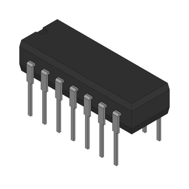
�Case outline X.
FIGURE 1. Case outline(s).
SIZE
STANDARD
MICROCIRCUIT DRAWING
DEFENSE SUPPLY CENTER COLUMBUS
COLUMBUS, OHIO 43216-5000
DSCC FORM 2234
APR 97
85030
A
REVISION LEVEL
F
SHEET
7
�Case outline X - Continued.
�
�
�
� Symbol
�
�
�
� A
�
� A1
�
�
� b
�
� �b
�
�
� D
�
� E
�
� E1
�
�
� e
�
� L
�
� L1
�
�
� Q
�
� S
�
� S1
�
�
� �
Dimensions
�
�
�
�
�
�
�
�
�
�
�
�
�
�
�
�
�
�
�
�
�
�
�
�
�
�
�
�
�
�
�
�
�
�
�
�
�
Inches
Min
.215
.175
.016
.016
.860
.490
.295
�
�
�
�
�
�
�
�
�
�
�
�
�
�
�
�
�
�
�
Max
.250
.215
.020
.020
.885
.520
.305
.100 BSC
.130
.150
.020
.100
.080
�
�
�
�
�
�
�
�
�
�
�
�
�
�
.255
.290
.035
.160
.180
�
�
�
�
�
�
�
�
�
�
�
�
�
�
�
�
�
�
�
�
�
�
�
�
�
�
�
�
�
�
�
�
�
�
�
�
�
�
�
�
�
�
�
�
�
�
�
�
�
�
�
�
�
�
�
�
�
�
�
�
�
�
�
�
�
�
�
�
�
�
�
�
�
�
Millimeters
Min
5.46
4.44
0.41
0.41
21.84
12.45
7.49
�
�
�
�
�
�
�
�
�
�
�
�
�
�
�
�
�
�
�
Max
6.35
5.46
0.51
0.51
22.48
13.21
7.75
2.54 BSC
3.30
3.81
0.51
2.54
2.03
�
�
�
�
�
�
�
�
�
�
�
�
�
�
6.48
7.37
0.89
4.07
4.57
Notes
8
4
4
7
5, 8
3
�
�
�
�
�
�
�
�
�
�
�
�
�
�
�
�
�
�
�
�
�
�
�
�
�
�
�
�
�
�
�
�
�
�
�
�
�
�
�
0�
15�
0�
15�
NOTES:
1. Index area: A notch, square-package corner, or a pin one index point shall be located adjacent to pin one and within
the shaded area shown. The manufacturer's identification shall not be used as a pin one identification mark.
2. Dimension Q shall be measured from the seating plane to the base plane.
3. This dimension allows for off-center lid, meniscus, and weld squash.
4. The basic pin spacing is .100 inch (2.54 mm) between centerlines. Each pin centerline shall be located within ±.010
inch (0.25 mm) of its exact longitudinal position relative to pins 1 and 14.
5. Dimension S1 is not used.
6. Lead center when a = 0�. E1 shall be measured at the centerline of the leads (see MIL-STD-1835).
7. All leads: Increase maximum limit by .003 inch (0.08 mm) measured at the widest diameter when lead finish A or B is
applied.
8. If this configuration is used, no polymer or organic materials shall be applied or molded to the bottom of the package or
cover the leads.
FIGURE 1. Case outline(s) - Continued.
SIZE
STANDARD
MICROCIRCUIT DRAWING
DEFENSE SUPPLY CENTER COLUMBUS
COLUMBUS, OHIO 43216-5000
DSCC FORM 2234
APR 97
85030
A
REVISION LEVEL
F
SHEET
8
�Case outline Y.
FIGURE 1. Case outline(s) - Continued.
SIZE
STANDARD
MICROCIRCUIT DRAWING
DEFENSE SUPPLY CENTER COLUMBUS
COLUMBUS, OHIO 43216-5000
DSCC FORM 2234
APR 97
85030
A
REVISION LEVEL
F
SHEET
9
�Case outline Y - Continued.
�
�
�
� Symbol
�
�
�
� A
�
� b
�
� b1
�
�
� c
�
� D
�
� E
�
� E1
�
�
� e
�
� L
�
� L1
�
�
� Q
�
� S
�
� S1
�
Dimensions
�
�
�
�
�
�
�
�
�
�
�
�
�
�
�
�
�
�
�
�
�
�
�
�
�
�
�
�
�
�
�
�
�
�
Inches
Min
.140
.014
.030
.008
.770
.480
.295
�
�
�
�
�
�
�
�
�
�
�
�
�
�
�
�
�
�
Max
.200
.023
.070
.015
.810
.510
.305
0.100 BSC
.150
.180
.015
--.060
�
�
�
�
�
�
�
�
�
�
�
�
.200
--.035
.137
---
�
�
�
�
�
�
�
�
�
�
�
�
�
�
�
�
�
�
�
�
�
�
�
�
�
�
�
�
�
�
�
�
�
�
�
�
�
�
�
�
�
�
�
�
�
�
�
�
�
�
�
�
�
�
�
�
�
�
�
�
�
�
�
�
�
�
�
�
Millimeters
Min
3.56
0.36
0.76
0.20
19.56
12.19
7.49
�
�
�
�
�
�
�
�
�
�
�
�
�
�
�
�
�
�
Max
5.08
0.58
1.78
0.38
20.57
12.95
7.75
2.54 BSC
�
� 5.08
�
� --�
�
� 0.89
�
� 3.48
�
� --�
3.81
4.57
0.38
--1.52
Notes
2
6
4, 7
3
5
5
�
�
�
�
�
�
�
�
�
�
�
�
�
�
�
�
�
�
�
�
�
�
�
�
�
�
�
�
�
�
�
�
�
�
�
�
NOTES:
1. Index area: A notch or a lead one identification mark is located adjacent to lead one.
2. The minimum limit for dimension b1 may be .023 inch (0.58 mm) for all four corner leads only.
3. Dimension Q shall be measured from the seating plane to the base plane.
4. The basic pin spacing is .100 inch (2.54 mm) between centerlines.
5. Applies to all four corners.
6. E1 shall be measured at the centerline of all the leads.
FIGURE 1. Case outline(s) - Continued.
SIZE
STANDARD
MICROCIRCUIT DRAWING
DEFENSE SUPPLY CENTER COLUMBUS
COLUMBUS, OHIO 43216-5000
DSCC FORM 2234
APR 97
85030
A
REVISION LEVEL
F
SHEET
10
�Device types 01 and 02.
�
�
�
�
�
�
�
�
�
�
�
�
�
�
�
�
�
�
�
�
�
�
�
�
�
�
�
�
�
�
�
�
�
�
�
�
2700
Terminal
number
Case
outlines
1
2
3
4
5
6
7
8
9
10
11
12
13
14
15
16
17
18
19
20
21
22
23
24
25
26
27
� 28
�
�
�
�
�
�
�
�
�
�
�
�
�
�
�
�
�
�
�
�
�
�
�
�
�
�
�
�
�
�
�
�
�
�
�
Terminal
symbol
�
�
C, X, Y
�
�
NC
�
NC
�
NC
�
NC
�
NC
�
NC
�
GND
�
NC
�
NC
�
TEST POINT �
VCC
�
+10 V ADJ
�
+10 V OUT �
+10 V ADJ
�
�
�
�
�
�
�
�
�
�
�
�
�
�
Z
Device types 03 and 04.
�
�
�
�
�
�
�
�
�
�
�
�
�
�
�
�
�
�
�
�
�
�
�
�
�
�
�
�
�
�
�
�
�
�
�
VO SEN
-IN
REF GND
GND SEN
NC
NC
NC
NC
NC
NC
NC
NC
NC
NC
NC
NC
NC
VZ
ZENER GND
NC
NC
VOS
VOS
POWER GND
VCC
+IN
VO FORCE
�
� +10 V REF OUT �
�
�
�
�
�
�
�
�
�
�
�
�
�
�
�
�
�
�
�
�
�
�
�
�
�
�
�
�
�
�
�
�
�
�
�
2702
Terminal
number
Case
outlines
1
2
3
4
5
6
7
8
9
10
11
12
13
14
15
16
17
18
19
20
21
22
23
24
25
26
� 27
� 28
�
�
�
�
�
�
�
�
�
�
�
�
�
�
�
�
�
�
�
�
�
�
�
�
�
�
�
�
�
�
�
�
�
�
�
Terminal
symbol
�
�
C, X, Y
�
�
-10 V ADJ
�
-10 V OUT
�
-10 V ADJ
�
VEE
�
NC
�
NC
�
GND
�
NC
�
NC
�
TEST POINT �
VCC
�
+10 V ADJ
�
+10 V OUT �
+10 V ADJ
�
�
�
�
�
�
�
�
�
�
�
�
�
Z
VO SEN
-IN
REF GND
GND SEN
NC
NC
-VOS
-VOS
VEE
+IN
VCC
NC
-IN
VO FORCE
-10 V REF OUT
VO SENSE
+10 V IN
VZ
ZENER GND
NC
NC
VOS
VOS
POWER GND
VCC
+IN
� VO FORCE
� +10 V REF OUT
�
�
�
�
�
�
�
�
�
�
�
�
�
�
�
�
�
�
�
�
�
�
�
�
�
�
�
�
�
�
�
�
�
�
�
�
�
FIGURE 2. Terminal connections.
SIZE
STANDARD
MICROCIRCUIT DRAWING
DEFENSE SUPPLY CENTER COLUMBUS
COLUMBUS, OHIO 43216-5000
DSCC FORM 2234
APR 97
85030
A
REVISION LEVEL
F
SHEET
11
�Device types 05 and 06.
�
�
�
�
�
�
�
�
�
�
�
�
�
�
�
�
�
�
�
�
�
�
�
�
�
�
�
�
�
�
�
�
�
�
�
�
�
�
�
�
Terminal
�
symbol
�
�
�
�
�
C, X, Y
�
Z
�
�
�
NC
� NC
�
NC
� NC
�
NC
� REF GND
�
NC
� GND SENSE �
NC
� NC
�
NC
� NC
�
GND
� -VOS
�
NC
� -VOS
�
NC
� VEE
�
TEST POINT � +IN
�
VEE
� NC
�
-10 V ADJ
� PWR GND
�
-10 V OUT � -IN
�
-10 V ADJ
� VO FORCE
�
� VO SENSE
�
� VO SENSE
�
� NC
�
� VZ
�
� ZENER GND �
� NC
�
� NC
�
� NC
�
� NC
�
� NC
�
� NC
�
� NC
�
� NC
�
� NC
�
2701
Terminal
number
Case
outlines
1
2
3
4
5
6
7
8
9
10
11
12
13
14
15
16
17
18
19
20
21
22
23
24
25
26
27
28
�
�
�
�
�
�
�
�
�
�
�
�
�
�
�
�
�
�
�
�
�
�
�
�
�
�
�
�
�
�
�
�
�
�
�
FIGURE 2. Terminal connections - Continued.
SIZE
STANDARD
MICROCIRCUIT DRAWING
DEFENSE SUPPLY CENTER COLUMBUS
COLUMBUS, OHIO 43216-5000
DSCC FORM 2234
APR 97
85030
A
REVISION LEVEL
F
SHEET
12
�Device types 01 and 02.
Device types 03 and 04.
FIGURE 3. Trim circuit(s).
SIZE
STANDARD
MICROCIRCUIT DRAWING
DEFENSE SUPPLY CENTER COLUMBUS
COLUMBUS, OHIO 43216-5000
DSCC FORM 2234
APR 97
85030
A
REVISION LEVEL
F
SHEET
13
�Device types 05 and 06.
NOTES:
1. External 10 k� potentiometer provides a ±20 mV minimum output offset adjust. Temperature effect is 4 µV/�C per mV
of offset correction (external adjustment optional).
2. Dual-in-line package only.
FIGURE 3. Trim circuit(s) - Continued.
SIZE
STANDARD
MICROCIRCUIT DRAWING
DEFENSE SUPPLY CENTER COLUMBUS
COLUMBUS, OHIO 43216-5000
DSCC FORM 2234
APR 97
85030
A
REVISION LEVEL
F
SHEET
14
�TABLE II. Electrical test requirements.
MIL-PRF-38534 test requirements
Subgroups
(in accordance with
MIL-PRF-38534, group
A test table)
Interim electrical parameters
----
Final electrical parameters
1*, 2, 3, 4
Group A test requirements
1, 2, 3, 4, 5, 6
Group C end-point electrical
parameters
1
* PDA applies to subgroup 1.
4.3 Conformance and periodic inspections. Conformance inspection (CI) and periodic inspection (PI) shall be in accordance
with MIL-PRF-38534 and as specified herein.
4.3.1 Group A inspection (CI). Group A inspection shall be in accordance with MIL-PRF-38534 and as follows:
a.
Tests shall be as specified in table II herein.
b.
Subgroups 7, 8, 10, and 11 shall be omitted.
4.3.2 Group B inspection (PI). Group B inspection shall be in accordance with MIL-PRF-38534.
4.3.3 Group C inspection (PI). Group C inspection shall be in accordance with MIL-PRF-38534 and as follows:
a.
End-point electrical parameters shall be as specified in table II herein.
b.
Steady-state life test, method 1005 of MIL-STD-883.
(1)
Test condition A, B, C, or D. The test circuit shall be maintained by the manufacturer under document revision level
control and shall be made available to either DSCC-VA or the acquiring activity upon request. Also, the test circuit
shall specify the inputs, outputs, biases, and power dissipation, as applicable, in accordance with the intent
specified in test method 1005 of MIL-STD-883.
(2)
TA as specified in accordance with table I of method 1005 of MIL-STD-883.
(3)
Test duration: 1,000 hours, except as permitted by method 1005 of MIL-STD-883.
4.3.4 Group D inspection (PI). Group D inspection shall be in accordance with MIL-PRF-38534.
SIZE
STANDARD
MICROCIRCUIT DRAWING
DEFENSE SUPPLY CENTER COLUMBUS
COLUMBUS, OHIO 43216-5000
DSCC FORM 2234
APR 97
85030
A
REVISION LEVEL
F
SHEET
15
�5. PACKAGING
5.1 Packaging requirements. The requirements for packaging shall be in accordance with MIL-PRF-38534.
6. NOTES
6.1 Intended use. Microcircuits conforming to this drawing are intended for use for Government microcircuit applications
(original equipment), design applications, and logistics purposes.
6.2 Replaceability. Microcircuits covered by this drawing will replace the same generic device covered by a
contractor-prepared specification or drawing.
6.3 Configuration control of SMD's. All proposed changes to existing SMD's will be coordinated with the users of record for
the individual documents. This coordination will be accomplished in accordance with MIL-STD-973 using DD Form 1692,
Engineering Change Proposal.
6.4 Record of users. Military and industrial users shall inform Defense Supply Center Columbus when a system application
requires configuration control and the applicable SMD. DSCC will maintain a record of users and this list will be used for
coordination and distribution of changes to the drawings. Users of drawings covering microelectronic devices (FSC 5962)
should contact DSCC-VA, telephone (614) 692-7603.
6.5 Comments. Comments on this drawing should be directed to DSCC-VA, P. O. Box 3990, Columbus, Ohio 43216-5000,
or telephone (614) 692-0676.
6.6 Sources of supply. Sources of supply are listed in QML-38534. The vendors listed in QML-38534 have submitted a
certificate of compliance (see 3.7 herein) to DSCC-VA and have agreed to this drawing.
SIZE
STANDARD
MICROCIRCUIT DRAWING
DEFENSE SUPPLY CENTER COLUMBUS
COLUMBUS, OHIO 43216-5000
DSCC FORM 2234
APR 97
85030
A
REVISION LEVEL
F
SHEET
16
�STANDARD MICROCIRCUIT DRAWING SOURCE APPROVAL BULLETIN
DATE: 99-01-08
Approved sources of supply for SMD 85030 are listed below for immediate acquisition only and shall be added to QML-38534
during the next revision. QML-38534 will be revised to include the addition or deletion of sources. The vendors listed below
have agreed to this drawing and a certificate of compliance has been submitted to and accepted by DSCC-VA. This bulletin is
superseded by the next dated revision of QML-38534.
Standard
microcircuit drawing
PIN 1/
Vendor
CAGE
number
Vendor
similar
PIN 2/
8503001CA
8505001CC
8503001XX
8503001YA
8503001YC
8503001YX
8503001YA
85030013A
33256
33256
3/
33256
33256
3/
34707
34707
HS2700SD
HS2700SD
2700SD/883B
HS2700SD
HS2700SD
2700SD/883B
HC2700SD/883B
HC2700SLCC/883B
8503002CA
8503002CC
8503002XX
8503002YA
8503002YC
8503002YX
8503002YA
85030023A
33256
33256
3/
33256
33256
3/
34707
34707
HS2700UD
HS2700UD
2700UD/883B
HS2700UD
HS2700UD
2700UD/883B
HC2700UD/883B
HC2700ULCC/883B
8503003CA
8503003CC
8503003XX
8503003YA
8503003YC
8503003YX
8503003YA
85030033A
33256
33256
3/
33256
33256
3/
34707
34707
HS2702SD
HS2702SD
2702SD/883B
HS2702SD
HS2702SD
2702SD/883B
HC2702SD/883B
HC2702SLCC/883B
8503004CA
8503004CC
8503004XX
8503004YA
8503004YC
8503004YX
8503004YA
85030043A
33256
33256
3/
33256
33256
3/
34707
34707
HS2702UD
HS2702UD
2702UD/883B
HS2702UD
HS2702UD
2702UD/883B
HC2702UD/883B
HC2702ULCC/883B
1/ The lead finish shown for each PIN, representing a hermetic package, is the most readily available from the
manufacturer listed for that part. If the desired lead finish is not listed contact the Vendor to determine availability.
2/ Caution. Do not use this number for item acquisition. Items acquired to this number may not satisfy the performance
requirements of this drawing.
3/ Not available from a QML source.
1 of 2
�STANDARD MICROCIRCUIT DRAWING SOURCE APPROVAL BULLETIN - Continued.
DATE: 99-01-08
Standard
microcircuit drawing
PIN 1/
Vendor
CAGE
number
Vendor
similar
PIN 2/
8503005CA
8503005CC
8503005XX
8503005YA
8503005YC
8503005YA
8503005YC
8503005YA
85030053A
33256
33256
3/
33256
33256
34031
34031
34707
34707
HS2701SD
HS2701SD
2701SD/883B
HS2701SD
HS2701SD
2701SD/883B
2701SD/883B
HC2701SD/883B
HC2701SLCC/883B
8503006CA
8503006CC
8503006XX
8503006YA
8503006YC
8503006YA
8503006YC
8503006YA
85030063A
33256
33256
3/
33256
33256
34031
34031
34707
34707
HS2701UD
HS2701UD
2701UD/883B
HS2701UD
HS2701UD
2701UD/883B
2701UD/883B
HC2701UD/883B
HC2701ULCC/883B
1/ The lead finish shown for each PIN, representing a hermetic package, is the most readily available from the
manufacturer listed for that part. If the desired lead finish is not listed contact the Vendor to determine availability.
2/ Caution. Do not use this number for item acquisition. Items acquired to this number may not satisfy the performance
requirements of this drawing.
3/ Not available from a QML source.
Vendor CAGE
number
Vendor name
and address
33256
Sipex Corporation
Hybrid Systems Division
22 Linnell Circle
Billerica, CA 01821-3985
34031
Analog Devices, Incorporated
7910 Triad Center Drive
Greensboro, NC 27409-9605
34707
Hycomp, Incorporated
165 Cedar Hill Street
Marlborough, MA 01752-3035
�
� The information contained herein is disseminated for convenience only and
� the Government assumes no liability whatsoever for any inaccuracies in this
� information bulletin.
�
2 of 2
�
�
�
�
�
�