One Technology Way · P.O. Box 9106 · Norwood, MA 02062-9106 · Tel: 781.329.4700 · Fax: 781.461.3113 · www.analog.com
ADI AD-FMCJESDADC1-EBZ Boards & Xilinx
Reference Design
Introduction
The AD-FMCJESDADC1-EBZ is a high speed data acquisition (4 ADC channels at 250MSPS), in an FMC
form factor, which has two high speed JESD-204B Analog to Digital converters (AD9250) on it.
This board is similar to the 4DSP FMC-176, which in addition to the AD9250, has two AD9129
DACs. This reference design works for either of the boards, for details see fmc-176_information
section.
Also included in this wiki is a dual AD-FMCJESDADC1-EBZ on
Dual AD-FMCJESDADC1-EBZ section.
VC707 reference design, for details see
The AD9250 is a dual, 14-bit ADC with sampling speeds of up to 250 MSPS. It features a multistage,
differential pipelined architecture with integrated output error correction logic. It supports wide
bandwidth inputs for a variety of user-selectable input ranges. The AD9250 features JESD204B high
speed serial interface.
The boards also feature the AD9517-1 for multi-output clock distribution with sub-picosecond jitter
performance, along with an on-chip PLL and VCO. The devices may be clocked by either an internal
clock source (optionally locked to an external reference) or an externally supplied sample clock.
It also features an external trigger input for customized sampling control. The card is mechanically
and electrically compliant to the FMC standard (ANSI/VITA 57.1).
The reference design includes the device data capture via the JESD204B serial interface and the SPI
interface. The samples are written to the external DDR-DRAM. It allows programming the device and
monitoring it's internal registers via SPI.
Supported Devices
●
AD-FMCJESDADC1-EBZ (ADI)
Rev 23 Apr 2013 22:21 | Page 1
�Supported Carriers
●
●
●
●
ML605
KC705
VC707
ZC706
Quick Start Guide
The reference design zip file contains a bit file combined with a SDK elf file for a quick demonstration
of the programming, RF conversion and data capture. All you need is the hardware and a PC running a
UART terminal and the programmer (IMPACT).
Required Hardware
●
●
●
ML605, KC705 or VC707 board
AD-FMCJESDADC1-EBZ
Signal generators (for ADC inputs)
Required Software
●
●
Xilinx ISE (Programmer (IMPACT) is sufficient for the demo and is available on Webpack).
A UART terminal (Tera Term/Hyperterminal), Baud rate 57600.
Bit file
●
Download the gzip file and extract the sw/cf_fmc176_kc705.bit file.
Running Demo (SDK) Program
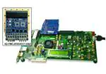
To begin make the following connections (see image below):
●
●
●
●
Connect the AD-FMCJESDADC1-EBZ board to the FMC-HPC connector of ML605/KC705 (FMC1-HPC if
VC707) board.
Connect power to ML605/KC705/VC707.
Connect two USB cables from the PC to the JTAG and UART USB connectors on ML605/KC705/VC707.
Connect signal generators to the A3, A2, A1 and/or A0 connectors.
Rev 23 Apr 2013 22:21 | Page 2
�The quick start bit file configures the AD9517 to generate 250MHz clock to AD9250. It runs both the
ADCs through all test modes and verifies the captured data accordingly. After the hardware setup,
turn the power on..
Start IMPACT, and initialze the JTAG chain. The program should recognize the 7 series device. Start a
UART terminal (set to 57600 baud rate) and then program the device. If programming was successful,
you should be seeing messages appear on the terminal as shown in figure below. After programming
the devices, the program checks data capture on various test modes.
After patterns and prbs sequences are verified, if no errors are present, you may use the chipscope
busplot to see the captured signal (see below). A chipscope project file is available inside the sw
directory.
Using the reference design
The reference design is built on a microblaze based system parameterized for linux. A functional block
diagram of the design is given below. The reference design contains both ADC and DAC pcores. If you
are using the AD-FMCJESDADC1-EBZ, you can ignore the DAC pcores.
Rev 23 Apr 2013 22:21 | Page 3
�The reference design consists of two identical instances of pcores for the DAC. On the ADC side, it
consists of a single JESD core (using Xilinx IP) and two identical instances of AD9250 pcores.
The AD9129 core consists of three functional modules, the DAC interface, a DDS (using Xilinx IP) and
a VDMA interface. The frequency of DDS may be set via the programming interface. Alternatively a
custom data sequence may be used via the VDMA interface.
The AD9250 core consists of three functional modules, the ADC interface, a PN9/PN23 monitor and a
DMA interface. The ADC interface captures and buffers data from the JESD core. The DMA interface
then transfers the samples to the external DDR-DRAM. The capture is initiated by the software. The
status of capture (overflow, over the range) are reported back to the software.
All the pcores have an AXI lite interface that allows control and monitoring of data generation and/or
capture.
The reference design also includes HDMI cores for GTX eye scan.
Registers
Please refer to the regmap.txt file in the pcores directory.
Changing ADC Sample Rates
The ADC sampling rate can vary from 40MHz to 250MHz. However, there are limitations imposed by
the FPGA that may lower this range. In some cases, you may have to regenerate the cores for a
different range. The reference design uses GTX (channel PLL) primitives and Xilinx's JESD core IP. The
default design runs at 250MHz clock (5Gbps rate).
Rev 23 Apr 2013 22:21 | Page 4
�As of this writing, the GTX specification & switching characteristics may be found at:
http://www.xilinx.com/support/documentation/user_guides/ug476_7Series_Transceivers.pdf
http://www.xilinx.com/support/documentation/data_sheets/ds182_Kintex_7_Data_Sheet.pdf
The key switching characteristics areThe reference clock has a range of 60MHz to 670MHz (700MHz). This limits the minimum sampling
clock to 60MHz. Though it is NOT recommended, it is possible to use AD9517 to generate a 40MHz
sampling clock to AD9250 and a 80MHz reference clock to the FPGA.
The line rate however, varies based on speed grade, package type and the use of CPLL vs QPLL. The
CPLL supports rates between 0.5Gbps to 6.6Gbps (the core may have to be changed for rates less
than 3.2Gbps (sampling rate 160MHz) - and the IP may not support all the combinations). Again, it is
possible to run the device on a single lane at a higher rate (rather than 2 lanes each at a lower rate)
to circumvent some of the troubles of line rate dependency on parametrization, package type and
speed grade.
You must carefully evaluate these specifications against your requirements to run the design at a
specific sampling frequency (or a range). As always, if you have any questions or run into any
problems, ask help & support.
JESD Interface
The default chipscope also captures the GTX/JESD core interface for a quick check on the transfer
phases. There is a simple state machine within the pcore that walks through all the phases of the
JESD specification. A sample screenshot is given below.
The default signals are:
The following signals are per lane (GTX). Refer to Xilinx documentation on details of these signals.
rx_data
GTX receive data (32 bits).
rx_notintable
GTX receive data not in table (invalid 8B/10B).
rx_disperr
GTX receive disparity error.
rx_charisk
GTX receive data is a K character .
rx_fsm
The state machine (see the pcore module for details).
rx_sync_enb
SYNC enable (SYNC is driven by JESD core, but is enabled by the state machine).
rx_sysref_enb
SYSREF enable (SYSREF is driven by all lanes at the end of CGS).
rx_valid_k
If set, indicates a valid 'K' character on received data.
rx_cgs_k
If set, indicates CGS data on received data.
rx_ilas_r
If set, indicates 'R' character on received data.
rx_ilas_a
If set, indicates 'A' character on received data.
rx_ilas_q
If set, indicates 'Q' character on received data.
rx_ilas_f
If set, indicates 'F' character on received data.
The following signals are top level signals (common to all lanes)
jesd204b_rxsync_s The sync is generated by the IP core.
Rev 23 Apr 2013 22:21 | Page 5
�gtx_rst_s
jesd204b_rst_s
rxsync
rxsysref
The GTX reset (software controlled).
The JESD core reset (software controlled AND GTX).
JESD204b SYNC
JESD204b SYSREF
After reset (0x0), the FSM is at state 0x1, where it waits for CGS (Code Group Synchronization). After
it finds a certain number of consecutive K characters (this ensures that the CGS phase is stable and
lanes are all up and running), it asserts SYSREF and also enables SYNC. At state 3, it waits for SYNC to
be deasserted. Note that enabling SYNC only allows the Xilinx core to drive the SYNC and do NOT
deassert SYNC. The SYNC is soon deasserted by the JESD core and the FSM moves to state 4. At state
4, it is assumed that it is correctly done by the Xilinx IP core. At any point, if SYNC is asserted by the
core, the process starts over.
Here is the sample screen shot:
FMC-176 Information
The 4DSP FMC-176 is a high speed data acquisition (4 ADC channels at 250MSPS) and conversion (2
DAC channels at 5.6GSPS) card. This card features two AD9250 and two AD9129.
The AD9129 is a high performance 14-bit RF DAC supporting data rates up to 2.8GSPS. The DAC core
is based on a quad-switch architecture that enables dual-edge clocking operation effectively
increasing the DAC update rate to 5.6 GSPS when configured for mix-mode or 2x interpolation. Its
high dynamic range and bandwidth enables multicarrier generation up to and beyond 4.2 GHz. The
AD9129 features two 14bit LVDS parallel interface.
The following variations of this board are available.
Part Number
ADC Channels DAC Channels
FMC-176
4 (2 x AD9250) 2 (2 x AD9129)
FMC-230
2 (2 x AD9129)
AD-FMCJESDADC1-EBZ 4 (2 x AD9250)
This reference design may be used as it is for FMC-176 and it's variations by selecting the appropriate
number of DAC channels. It is also easy to port the design for other boards by removing one or more
corresponding pcores. Also some devices may not be accessible depending on whether one choose to
use LPC or HPC. To fully support both the DACs of the FMC-176, a carrier must have a fully populated
HPC connector. The KC705 do not have a fully populated HPC.
The reference design includes (if enabled) RF generation via DDS and the SPI interface for the DACs.
At the prompt just enter the number of DAC channels you have in your hardware setup. As an
Rev 23 Apr 2013 22:21 | Page 6
�example, if you are using FMC-176 with KC705, simply enter '1' as the number of DAC channels. If you
are using the ADC only boards, enter '0' as the number of DAC channels.
The quick start bit file also configures the AD9517 to generate a 2.5GHz clock to AD9129. It then
generates a 333MHz tone for the DAC.
The DAC spectrum for a 333MHz tone is shown below.
It is possible to use an adapter board such as FMC-700 with KC705 to access both
the DACs on a FMC-176 board. However, the routing delays of FMC-LPC pins to
the FMC-700 will cause timing errors on DAC1 and you may see parity errors on
the UART terminal.
Dual AD-FMCJESDADC1-EBZ
In the downloads section, you will also find a dual AD-FMCJESDADC1-EBZ reference design for VC707.
This design supports two AD-FMCJESDADC1-EBZ (4 x AD9250 devices) on VC707 using both the FMC1
and FMC2 connectors. It does NOT support any variations that includes AD9129.
The procedure is the same. The setup, UART and chipscope plots are shown below.
Rev 23 Apr 2013 22:21 | Page 7
�Downloads
FPGA Referece Designs:
●
●
●
●
●
ML605
KC705
VC707
VC707
ZC706
cf_fmc176_ml605_edk_14_4_2013_04_04.tar.gz
cf_fmc176_kc705_edk_14_4_2013_04_04.tar.gz
cf_fmc176_vc707_edk_14_4_2013_04_04.tar.gz
cf_fmc176x2_vc707_edk_14_4_2013_04_04.tar.gz
cf_fmc176_zc706_edk_14_4_2013_04_04.tar.gz
Software Files:
●
●
●
●
●
ML605
KC705
VC707
VC707
ZC706
cf_fmc176_ml605_sw_14_4_2013_04_04.tar.gz
cf_fmc176_kc705_sw_14_4_2013_04_04.tar.gz
cf_fmc176_vc707_sw_14_4_2013_04_04.tar.gz
cf_fmc176x2_vc707_sw_14_4_2013_04_04.tar.gz
cf_fmc176_zc706_sw_14_4_2013_04_04.tar.gz
Only Xilinx coregen xco files are provided with the reference design. You must regenerate the IP core
files using this file. See generating Xilinx netlist/verilog files from xco files for details.
●
Questions? Ask Help & Support.
Rev 23 Apr 2013 22:21 | Page 8
�Tar file contents
The tar file contains, in most cases, the following files and/or directories. To rebuild the reference
design simply double click the XMP file and run the tool. To build SDK, select a workspace and use the
C file to build the elf file. Please refer to Xilinx EDK documentation for details.
license.txt
system.mhs
system.xmp
data/
ADI license & copyright information.
MHS file.
XMP file (use this file to build the reference design).
UCF file and/or DDR MIG project files.
Documentation files (Please note that this wiki page is the documentation for the
docs/
reference design).
sw/
Software (Xilinx SDK) & bit file(s).
cf_lib/edk/pcores/ Reference design core file(s) (Xilinx EDK).
More information
●
●
VITA's FMC info
Ask questions about the FPGA reference design
© Analog Devices, Inc. All rights reserved. Trademarks and
registered trademarks are the property of their respective owners.
Rev 23 Apr 2013 22:21 | Page 9
www.analog.com
�