a
Complete Dual 18-Bit
16 ⴛ FS Audio DAC
AD1865*
FUNCTIONAL BLOCK DIAGRAM
(DIP Package)
FEATURES
Dual Serial Input, Voltage Output DACs
No External Components Required
110 dB SNR
0.003% THD+N
Operates at 16 ⴛ Oversampling per Channel
ⴞ5 Volt Operation
Cophased Outputs
116 dB Channel Separation
Pin Compatible with AD1864
DIP or SOIC Packaging
APPLICATIONS
Multichannel Audio Applications
Compact Disc Players
Multivoice Keyboard Instruments
DAT Players and Recorders
Digital Mixing Consoles
Multimedia Workstations
–V S
1
TRIM
2
23 TRIM
REFERENCE
MSB
24 +V S
AD1865
REFERENCE
3
22
MSB
IOUT
IOUT
4
21
AGND
5
20
AGND
19
SJ
SJ
6
RF
7
18
RF
VOUT
8
17
VOUT
+VL
9
16
NC
DR
10
15
DL
LR
11
14
LL
13
DGND
CLK
18-BIT
LATCH
18-BIT
D/A
18-BIT
D/A
12
18-BIT
LATCH
NC = NO CONNECT
PRODUCT DESCRIPTION
The AD1865 is a complete, dual 18-bit DAC offering excellent
THD+N and SNR while requiring no external components. Two
complete signal channels are included. This results in cophased
voltage or current output signals and eliminates the need for
output demultiplexing circuitry. The monolithic AD1865 chip
includes CMOS logic elements, bipolar and MOS linear elements and laser-trimmed thin-film resistor elements, all fabricated on Analog Devices’ ABCMOS process.
The DACs on the AD1865 chip employ a partially segmented
architecture. The first four MSBs of each DAC are segmented
into 15 elements. The 14 LSBs are produced using standard R-2R
techniques. Segment and R-2R resistors are laser trimmed to provide extremely low total harmonic distortion. This architecture
minimizes errors at major code transitions resulting in low output glitch and eliminating the need for an external deglitcher.
When used in the current output mode, the AD1865 provides
two ± 1 mA output signals.
Each channel is equipped with a high performance output amplifier. These amplifiers achieve fast settling and high slew rate,
producing ± 3 V signals at load currents up to 8 mA. Each output amplifier is short-circuit protected and can withstand indefinite short circuits to ground.
The AD1865 was designed to balance two sets of opposing requirements, channel separation and DAC matching. High channel separation is the result of careful layout. At the same time,
both channels of the AD1865 have been designed to ensure
matched gain and linearity as well as tracking over time and
temperature. This assures optimum performance when used in
stereo and multi-DAC per channel applications.
A versatile digital interface allows the AD1865 to be directly
connected to standard digital filter chips. This interface employs
five signals: Data Left (DL), Data Right (DR), Latch Left (LL),
Latch Right (LR) and Clock (CLK). DL and DR are the serial
input pins for the left and right DAC input registers. Input data
bits are clocked into the input register on the rising edge of
CLK. A low-going latch edge updates the respective DAC output. For systems using only a single latch signal, LL and LR
may be connected together. For systems using only one DATA
signal, DR and DL may be connected together.
The AD1865 operates with ± 5 V power supplies. The digital
supply, VL, can be separated from the analog supplies, VS and
–VS, for reduced digital feedthrough. Separate analog and digital
ground pins are also provided. The AD1865 typically dissipates
only 225 mW, with a maximum power dissipation of 260 mW.
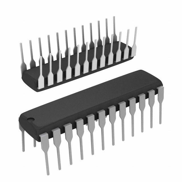
The AD1865 is packaged in both a 24-pin plastic DIP and a
28-pin SOIC package. Operation is guaranteed over the temperature range of –25°C to +70°C and over the voltage supply
range of ± 4.75 V to ± 5.25 V.
PRODUCT HIGHLIGHTS
REV. 0
11.
12.
13.
14.
15.
16.
17.
18.
19.
10.
Information furnished by Analog Devices is believed to be accurate and
reliable. However, no responsibility is assumed by Analog Devices for its
use, nor for any infringements of patents or other rights of third parties
which may result from its use. No license is granted by implication or
otherwise under any patent or patent rights of Analog Devices.
One Technology Way, P.O. Box 9106, Norwood, MA 02062-9106, U.S.A.
Tel: 617/329-4700
Fax: 617/326-8703
*Protected by U.S. Patents Nos.: RE 30,586; 3,961,326; 4,141,004;
4,349,811; 4,855,618; 4,857,862.
The AD1865 is a complete dual 18-bit audio DAC.
110 dB signal-to-noise ratio for low noise operation.
THD+N is typically 0.003%.
Interchannel gain and midscale matching.
Output voltages and currents are cophased.
Low glitch for improved sound quality.
Both channels are 100% tested at 16 × FS.
Low Power—only 225 mW typ, 260 mW max.
Five-wire interface for individual DAC control.
24-pin DIP or 28-pin SOIC packages available.
�= +25ⴗC, +V = +V = +5 V and –V = –5 V, F = 705.6 kHz, no MSB adjustment
AD1865–SPECIFICATIONS or(T deglitcher)
A
L
Parameter
S
S
Min
RESOLUTION
S
Typ
Max
18
DIGITAL INPUTS VIH
VIL
IIH, VIH = +VL
IIL, VIL = 0.4 V
Clock Input Frequency
2.0
Bits
+VL
0.8
1.0
–10
V
V
µA
µA
MHz
1.0
0.8
% of FSR
% of FSR
mV
mV
dB
13.5
ACCURACY
Gain Error
Interchannel Gain Matching
Midscale Error
Interchannel Midscale Matching
Gain Linearity (0 dB to –90 dB)
0.2
0.3
4
5
74.1ns
>30ns
>30ns
CLK
>40ns
>40ns
>15ns
>40ns
LL/LR
>15ns
>15ns
DL/DR
>30ns
MSB
1st BIT
INTERNAL DAC INPUT REGISTER
UPDATED WITH 18 MOST RECENT BITS
2nd BIT
LSB
18th BIT
NEXT
WORD
BITS CLOCKED
TO SHIFT REGISTER
Figure 9. AD1865 Timing Diagram
REV. 0
–7–
�AD1865
–5V ANALOG SUPPLY
SM5813AP/
APT
+5V ANALOG SUPPLY
AD1865
28
1
–VS
+VS 24
2
27
2
TRIM
TRIM 23
3
BCKO 26
3
MSB
MSB 22
4
WCKO 25
4
IOUT
IOUT 21
5
DOL 24
5
AGND
6
DOR
23
6
SJ
SJ 19
7
VDD
22
7
RF
VSS2
21
8
VOUT
1
8
9
VSS1
DG
10
11
12
OW18
13
OW20
14
C1
AGND 20
1
+VS 8
RF 18
2
7
VOUT 17
3
6
NC 16
4
20
9
19
10 DR
DL 15
18
11 LR
LL 14
17
12 CLK
+VL
LEFT
CHANNEL
OUTPUT
C2
RIGHT
CHANNEL
OUTPUT
5
–VS
NE5532
DGND 13
16
15
+5V DIGITAL
SUPPLY
Figure 10. Complete 8 × FS 18-Bit CD Player
18-BIT CD PLAYER DESIGN
Figure 10 illustrates an 18-bit CD player design incorporating
an AD1865 D/A converter, an NE5532 dual op amp and the
SM5813 digital filter chip manufactured by NPC. In this design, the SM5813 filter transmits left and right digital data to
both channels of the AD1865. The left and right latch signals,
LL and LR, are both provided by the word clock signal
(WCKO) of the digital filter. The digital filter supplies data at
an 8 × FS oversample rate to each channel.
The digital data is converted to analog output voltages by the
output amplifiers on the AD1865. Note that no external components are required by the AD1865. Also, no deglitching circuitry is required.
An NE5532 dual op amp is used to provide the output antialias
filters required for adequate image rejection. One 2-pole filter
section is provided for each channel. An additional pole is created from the combination of the internal feedback resistors
(RF) and the external capacitors C1 and C2. For example, the
nominal 3 kΩ RF with a 360 pF capacitor for C1 and C2 will
place a pole at approximately 147 kHz, effectively eliminating
all high frequency noise components.
Low distortion, superior channel separation, low power consumption and a low parts count are all realized by this simple
design.
–8–
REV. 0
�AD1865
In this application, the advantages of choosing the AD1865 are
clear. Its flexible digital interface allows the clock and data to be
shared among all DACs. This reduces PC board area requirements and also simplifies the actual layout of the board. The low
power requirements of the AD1865 (approximately 225 mW) is
an advantage in a multiple DAC system where any power advantage is multiplied by the number of DACs used. The AD1865
requires no external components, simplifying the design, reducing the total number of components required and enhancing
reliability.
MULTICHANNEL DIGITAL KEYBOARD DESIGN
Figure 11 illustrates how to cascade AD1865’s to add multiple
voices to an electronic musical instrument. In this example, the
data and clock signals are shared between all six DACs. As the
data representing an output for a specific voice is loaded, the appropriate DAC is updated. For example, after the 18-bits representing the next output value for Voice 4 is clocked out on the
data line, then “Voice 4 Load” is pulled low. This produces a
new output for Voice 4. Furthermore, all voices can be returned
to the same output by pulling all six load signals low.
VOICE 2
OUTPUT
VOICE 1
OUTPUT
VOICE 3
OUTPUT
VOICE 4
OUTPUT
VOICE 5
OUTPUT
VOICE 6
OUTPUT
+5V ANALOG
SUPPLY
–5V ANALOG
SUPPLY
AD1865
AD1865
1 –V S
2
ANALOG
COMMON
TRIM
24
1
–V S
TRIM
23
2
TRIM
AD1865
+V S
24
1
–VS
TRIM
23
2
TRIM
3
MSB
MSB 22
21
4
IOUT
IOUT
AGND 20
5
AGND
SJ 19
6
SJ
RF
3 MSB
MSB
22
3
MSB
MSB 22
4
IOUT
IOUT
21
4
IOUT
IOUT
5
AGND
AGND
20
5
AGND
SJ
19
6
SJ
RF
RF
6 SJ
7
8
RF
VOUT
9 +VL
VOICE 1 LOAD
+VS
+V S
24
TRIM
23
21
AGND 20
SJ 19
RF 18
7
VOUT 17
8
VOUT
+VL
NC 16
9
+VL
NC 16
18
7
VOUT
17
8
VOUT
NC
16
9
RF
18
VOUT 17
10 DR
DL
15
10
DR
DL 15
10
DR
DL 15
11 LR
LL
14
11 LR
LL 14
11
LR
LL 14
DGND 13
12
CLK
12 CLK
DGND 13
12
CLK
DGND
VOICE 6 LOAD
13
VOICE 2 LOAD
VOICE 5 LOAD
VOICE 3 LOAD
VOICE 4 LOAD
DATA
CLOCK
DIGITAL COMMON
+5V DIGITAL SUPPLY
Figure 11. Cascaded AD1865s in a Multichannel Keyboard Instrument
REV. 0
–9–
�AD1865
ADDITIONAL APPLICATIONS
–5V ANALOG
SUPPLY
Figures 12 through 14 show connection diagrams for the AD1865
and standard digital filter chips from Yamaha, NPC and Sony.
Each figure is an example of cophase operation operating at 8 ×
FS for each channel. The 2-pole Rauch low-pass filters shown in
Figure 10 can be used with all of the applications shown in this
data sheet.
+5V ANALOG
SUPPLY
AD1865
1
+VS 24
–V
S
2
TRIM
3 MSB
2
3
4
V
DD2
GND
TEST 40
2
TEST
TEST 39
3
TEST 38
4
TEST 37
5
36
1 –V
S
16.9344
MHz
CXD1244S
35
2
TRIM
TRIM 23
3
MSB
MSB 22
8
BCKO 33
4
IOUT
9
XIN
DATAL 32
10 V
DD
11 VDD
GND 31
6 SJ
SJ 19
GND 30
7 R
RF 18
DATAR 29
12
13
28
9
+VL
14
LE/WS 27
10 DR
15
OUT 16/18 26
11 LR
16
25
17 LFS
12 CLK
NC 16
DL 15
OUT
L
6
WCO 11
11 LR
7
DRO 10
12 CLK
DLO
LL 14
DGND 13
9
LPF
RIGHT
CHANNEL
OUTPUT
LPF
LEFT
CHANNEL
OUTPUT
IOUT 21
AGND 20
F
8 V
OUT
+V
24
34
5 AGND
V
9
Figure 12. AD1865 with Yamaha YM3434 Digital Filter
S
7
6
8
13
SS
LEFT
CHANNEL
OUTPUT
VOUT 17
ST 14
V
LPF
+5V DIGITAL SUPPLY
AD1865
+V
RF 18
10 DR
+5V ANALOG
SUPPLY
–5V ANALOG
SUPPLY
SJ 19
BCO 12
DD1
1
SJ
5
8 V
OUT
AGND 20
7 R
F
6
SHR 16
16/18 15
21
I
5 AGND
YM3434
SHL
RIGHT
CHANNEL
OUTPUT
MSB 22
4 IOUT
1
LPF
23
TRIM
V
OUT
17
NC 16
DL 15
LL 14
DGND 13
DPOL 24
18 SONY/12S
23
19
TEST 22
20 TEST
TEST 21
–5V ANALOG
SUPPLY
+5V ANALOG
SUPPLY
AD1865
1 –V S
+5V DIGITAL SUPPLY
2 TRIM
Figure 13. AD1865 with Sony CXD1244s Digital Filter
3 MSB
SM5818
4
IOUT
5
AGND
1
VDD 16
6 SJ
2
BCKO 15
7
RF
8
VOUT
+VS 24
TRIM
23
RIGHT
CHANNEL
OUTPUT
LPF
LEFT
CHANNEL
OUTPUT
MSB 22
IOUT 21
AGND 20
SJ 19
RF
18
VOUT
17
3
WDCO 14
4
OMOD2 13
9 +VL
NC 16
5
DOR 12
10 DR
DL 15
6
DOL 11
11 LR
7
10
12 CLK
LPF
LL 14
DGND 13
8 VSS OMOD1 9
+5V DIGITAL SUPPLY
Figure 14. AD1865 with NPC SM5818AP Digital Filter
–10–
REV. 0
�AD1865
OTHER DIGITAL AUDIO COMPONENTS AVAILABLE
FROM ANALOG DEVICES
–VS
1
DGND
2
+VL
3
NC
4
CLK
5
LE
6
DATA
7
–VL
8
16-BIT
LATCH
16-BIT
DAC
AD1856 16-BIT AUDIO DAC
16 +VS
15 TRIM
SERIAL
INPUT
REGISTER
14 MSB ADJ
IOUT
REF
CONTROL
LOGIC
13 IOUT
Complete, No External Components Required
0.0025% THD
Low Cost
16-Pin DIP or SOIC Package
Standard Pinout
12 AGND
11 SJ
10 RF
AD1856
9
VOUT
NC = NO CONNECT
–VS
1
DGND
2
+VL
3
NC
4
CLK
5
LE
6
DATA
7
–VL
8
18-BIT
LATCH
18-BIT
DAC
AD1860 18-BIT AUDIO DAC
16 +VS
15 TRIM
SERIAL
INPUT
REGISTER
14 MSB ADJ
IOUT
REF
CONTROL
LOGIC
13 IOUT
Complete, No External Components Required
0.0025% THD+N
108 dB Signal-to-Noise Ratio
16-Pin DIP or SOIC Package
Standard Pinout
12 AGND
11 SJ
10 RF
AD1860
9
VOUT
NC = NO CONNECT
AD1862 20-BIT AUDIO DAC
REV. 0
–VS
1
–VS
2
15 NR2
TRIM
3
14 ADJ
+VL
4
13 NR1
CLK
5
LE
6
DATA
7
–VL
8
VL
1
LL
2
DL
3
CLK
4
DR
5
LR
6
DGND
7
VBIAS R
8
VOLTAGE
REFERENCE
16 +VS
119 dB Signal-to-Noise Ratio
0.0016% THD+N
102 dB D-Range Performance
± 1 dB Gain Linearity
16-Pin DIP Package
12 AGND
INPUT
&
DIGITAL
OFFSET
20-BIT
DAC
11 IOUT
10 RF
AD1862
18-BIT
DAC
9
AD1868
18-BIT
SERIAL
REGISTER
VREF
18-BIT
SERIAL
REGISTER
18-BIT
DAC
DGND
VREF
16
VBIAS L
15
VS
14
VOUT L
13
NRL
12
AGND
11
NRR
10
VOUT R
9
AD1868 +5 V SINGLE SUPPLY DUAL 18-BIT
AUDIO DAC
No External Components Required
0.004% THD+N
92 dB D-Range Performance
± 3 dB Gain Linearity
16-Pin DIP or SOIC Package
VS
–11–
�AD1865
OUTLINE DIMENSIONS
Dimensions shown in inches and (mm).
24
C1468–8–8/91
24-Pin Plastic DIP
(N-24A) Package
13
0.580 (14.73)
0.485 (12.32)
PIN 1
1
12
1.290 (32.70)
1.150 (29.30)
0.250 (6.35)
SEATING
PLANE
0.200 (5.05)
0.125 (3.18)
0.022 (0.558)
0.014 (0.356)
0.625 (15.87)
0.600 (15.24)
0.060 (1.52)
0.015 (0.38)
0.195 (4.95)
0.125 (3.18)
0.015 (0.381)
0.008 (0.204)
0.150
(3.81)
0.070 (1.77)
0.030 (0.77)
0.100 (2.54)
BSC
28-Pin SOIC
(R-28) Package
0.708 (18.02)
0.696 (17.67)
15
28
0.299 (7.6)
0.291 (7.39)
0.414 (10.52)
0.398 (10.10)
14
1
0.003 (0.76)
0.02 (0.51)
0.096 (2.44)
0.089 (2.26)
0.019 (0.49)
0.014 (0.35)
0.01 (0.254)
0.006 (0.15)
0.013 (0.32)
0.009 (0.23)
0.042 (0.32)
0.009 (0.23)
6°
0°
PRINTED IN U.S.A.
0.050 (1.27) BSC
–12–
REV. 0
�Package/Price Information
Complete Dual 18-Bit 16 3 FS Audio DAC
Model
Status
Package
Description
Pin
Count
Temperature
Range
Price*
(100-499)
AD1865N
PRODUCTION
PLASTIC/EPOXY DIP
24
COMMERCIAL
$16.34
AD1865N-J
PRODUCTION
PLASTIC/EPOXY DIP
24
COMMERCIAL
$19.64
AD1865N-K
PRODUCTION
PLASTIC/EPOXY DIP
24
COMMERCIAL
$25.49
AD1865P
PRODUCTION
PLASTIC LEAD CHIP CARRIER
28
COMMERCIAL
$16.34
AD1865R
PRODUCTION
STD S.O. PKG (SOIC)
28
COMMERCIAL
$16.34
* This price is provided for budgetary purposes as recommended list price in U.S. Dollars per unit in the stated volume. Pricing displayed for Evaluation
Boards and Kits is based on 1-piece pricing. View Pricing and Availability for further information.
�