Data Sheet
AD3551R
Single Channel, 16-Bit, 33 MUPS, Multispan, Multi-IO SPI DAC
FEATURES
►
►
►
►
►
►
►
►
►
►
►
►
►
►
GENERAL DESCRIPTION
16-bit resolution
33 MUPS rate in fast mode
22 MUPS rate in precision mode
65 ns small signal settling time to 0.1% accuracy
100 ns large signal settling time to 0.1% accuracy
Ultra small glitch: < 50 pV×s
Ultra low latency: 5 ns
THD: −105 dB at 1 kHz
Highly configurable output voltage span and offset
1.2 V and 1.8 V logic level compatible
Single (classic), dual, and quad SPI modes
Multiple error detectors, both analog and digital domains
2.5 V internal voltage reference, 10 ppm/°C maximum temperature coefficient
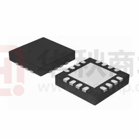
5 mm × 5 mm LFCSP
The AD3551R is a low drift, single channel, ultra-fast, 16-bit accuracy, current output digital-to-analog converter (DAC) that can be
configured in multiple voltage span ranges. The AD3551R operates
with a fixed 2.5 V reference.
Each DAC incorporates three drift compensating feedback resistors
for the required external transimpedance amplifier (TIA) that scales
the output voltage. Offset and gain scaling registers allow for
generation of multiple output span ranges, such as 0 V to 2.5 V, 0 V
to 5 V, 0 V to 10 V, −5 V to +5 V, and −10 V to +10 V, and custom
intermediate ranges with full 16-bit resolution.
The DAC can operate in fast mode for maximum speed or precision
mode for maximum accuracy.
The serial peripheral interface (SPI) can be configured in quad
SPI mode, dual SPI mode, and single SPI (classic SPI) mode with
single date rate (SDR) or double data rate (DDR), with logical levels
from 1.2 V to 1.8 V.
APPLICATIONS
►
►
►
►
►
►
►
►
The AD3551R is specified over the extended industrial temperature
range (–40°C to +105°C).
Instrumentation
Hardware in the loop
Process control equipment
Medical devices
Automated test equipment
Data acquisition system
Programmable voltage sources
Optical communications
Table 1. Related Devices
Part No.
Description
AD8675
36 V precision, 2.8 nV/√Hz rail-to-rail output operational amplifier
AD8065
High performance, 145 MHz FastFET™ operational amplifiers
ADA4807-1
3.1 nV/√Hz, 1 mA, 180 MHz, rail-to-rail input/output amplifier
LTC6655
0.25 ppm noise, low drift precision reference
ADR4525
Ultralow noise, high accuracy, 2.5 V voltage reference
FUNCTIONAL BLOCK DIAGRAM
Figure 1.
Analog Devices is in the process of updating documentation to provide terminology and language that is culturally appropriate. This is a process
with a wide scope and will be phased in as quickly as possible. Thank you for your patience.
Rev. A
DOCUMENT FEEDBACK
TECHNICAL SUPPORT
Information furnished by Analog Devices is believed to be accurate and reliable "as is". However, no responsibility is assumed by Analog
Devices for its use, nor for any infringements of patents or other rights of third parties that may result from its use. Specifications subject to
change without notice. No license is granted by implication or otherwise under any patent or patent rights of Analog Devices. Trademarks and
registered trademarks are the property of their respective owners.
�Data Sheet
AD3551R
TABLE OF CONTENTS
Features................................................................ 1
Applications........................................................... 1
General Description...............................................1
Functional Block Diagram......................................1
Specifications........................................................ 4
Electrical Characteristics.................................... 4
AC Characteristics..............................................5
Timing Characteristics........................................6
Absolute Maximum Ratings.................................10
Thermal Resistance......................................... 10
ESD Caution.....................................................10
Pin Configuration and Function Descriptions.......11
Typical Performance Characteristics................... 12
Terminology......................................................... 21
Theory of Operation.............................................22
Product Description.......................................... 22
DAC Architecture..............................................22
Predefined Output Voltage Spans.................... 22
Custom Output Voltage Span...........................23
Transfer Function............................................. 23
VREF..................................................................23
SPI Register Map Access.................................23
Serial Interface................................................. 30
DAC Update Modes......................................... 32
Power-Down.....................................................33
Reset................................................................ 33
Error Detection................................................. 33
ALERT Pin........................................................34
Device ID..........................................................35
Summary of Interface Access Modes...............35
Registers............................................................. 36
Register Summary............................................36
Interface Register Details................................. 39
DAC Register Details....................................... 48
Applications Information...................................... 57
Power Supply Recommendations.................... 57
Layout Guidelines.............................................57
Outline Dimensions............................................. 59
Ordering Guide.................................................59
Evaluation Boards............................................ 59
REVISION HISTORY
3/2023—Rev. 0 to Rev. A
Changed 16-Bit, 33 MUPS, Multispan, Multi-IO SPI DAC to Single Channel, 16-Bit, 33 MUPS,
Multispan, Multi-IO SPI DAC..........................................................................................................................1
Changed DVDD to DVDD, IOVDD to VLOGIC, VREF to VREF, AVDD to AVDD, VDD to AVDD (Throughout)......1
Changes to General Description Section and Table 1..................................................................................... 1
Changes to Table 2.......................................................................................................................................... 4
Changes to Table 3.......................................................................................................................................... 5
Changes to Table 5........................................................................................................................................ 10
Changes to Figure 12 and Table 7................................................................................................................. 11
Deleted Figure 51; Renumbered Sequentially............................................................................................... 18
Added Figure 65 and Figure 66; Renumbered Sequentially..........................................................................20
Changes to Relative Accuracy or Integral Nonlinearity (INL) Section............................................................21
Changes to Differential Nonlinearity (DNL) Section.......................................................................................21
Change to DC PSRR and AC PSRR Section................................................................................................ 21
Changes to Output Voltage Settling Time Section.........................................................................................21
Changes to Digital-to-Analog Glitch Impulse Section.................................................................................... 21
Changes to Digital Feedthrough Section....................................................................................................... 21
Changes to Output Noise Spectral Density Section...................................................................................... 21
Changes to Total Harmonic Distortion (THD) Section....................................................................................21
Changes to Product Description Section....................................................................................................... 22
Changes to DAC Architecture and Figure 67.................................................................................................22
Changes to Predefined Output Voltage Spans and Table 8...........................................................................22
Changes to Custom Output Voltage Span Section ....................................................................................... 23
Added Table 9 and Table 10; Renumbered Sequentially .............................................................................. 23
Changes to Transfer Function Section ..........................................................................................................23
Change to SPI Frame Synchronization Section ............................................................................................23
analog.com
Rev. A | 2 of 59
�Data Sheet
AD3551R
TABLE OF CONTENTS
Change to Figure 72...................................................................................................................................... 25
Changes to Streaming Mode Section............................................................................................................ 26
Changes to Figure 74 Caption and Figure 75................................................................................................27
Change to Figure 80...................................................................................................................................... 30
Change to Figure 81...................................................................................................................................... 30
Change to Figure 82...................................................................................................................................... 31
Changes to Register Map SPI Access Modes Section and Figure 86...........................................................32
Changes to SDIO Drive Strength...................................................................................................................32
Change to Figure 88...................................................................................................................................... 32
Changes to Table 15...................................................................................................................................... 33
Changes to Power-Down Section.................................................................................................................. 33
Changes to Reset Pin Section....................................................................................................................... 33
Changes to VREF Detection Section...............................................................................................................34
Changes to SPI Mode Error Section..............................................................................................................34
Changes to SPI Clock Counter Section ........................................................................................................ 34
Changes to Table 19...................................................................................................................................... 37
Changes to Channel 0 Gain Register Section and Table 42..........................................................................51
Changes to Power Supply Recommendations Section and Figure 91.......................................................... 57
Changes to Layout Guidelines Section .........................................................................................................57
2/2022—Revision 0: Initial Version
analog.com
Rev. A | 3 of 59
�Data Sheet
AD3551R
SPECIFICATIONS
ELECTRICAL CHARACTERISTICS
AVDD = 5.0 V ± 5%, DVDD = 1.8 V ± 5%, 1.1 V ≤ VLOGIC ≤ 1.9 V, VREF = 2.5 V, −40°C ≤ TA ≤ +105°C, output amplifier AD8675, unless otherwise
noted.
Table 2.
Parameter1
Symbol
STATIC PERFORMANCE
Resolution
Relative Accuracy (INL)
Differential Nonlinearity (DNL)
Min
Max
Unit
16
−2
−4
−1
+2
+4
+1
Bits
LSB
LSB
LSB
−2
+2
LSB
−2
+2
0.6
LSB
%FSR
ppm FSR/°C
ppm FSR/°C
%FSR
ppm FSR/°C
ppm FSR/°C
%FSR
ppm FSR/°C
ppm FSR/°C
%FSR
mV/V
1.6
mA
Absolute value
V
ppm/°C
At 25°C, over lifetime
Offset Error
Offset Error Drift2
0.03
2
4
0.04
1
4
0.05
3.5
7
Full-Scale Error
Full-Scale Error Drift2
Zero-Scale Error3
Zero-Scale Error Drift2
Total Unadjusted Error (TUE)
DC Power Supply Rejection Ratio (PSRR)
OUTPUT CHARACTERISTICS
Output Current
IOUTx
REFERENCE OUTPUT
Output Voltage
Voltage Reference Temperature
Coefficient (TC)4
Output Impedance
Output Voltage Noise
Output Voltage Noise Density
Capacitive Load Stability2
Load Regulation
Output Current Load Capability
Line Regulation
REFERENCE INPUT
Reference Current
Reference Input Range2
Reference Input Impedance
LOGIC INPUTS
Input Current
Input Low Voltage
−0.5
2.492
2.5
3
8
16
5
12
8
16
+0.5
2.508
10
50
2.7
173
164
10
50
±8
135
VREF
2.4
II
VIL
−1
Input High Voltage
VIH
0.65 ×
VLOGIC
Pin Capacitance
CI
analog.com
Typ
1
2.5
3
2.6
+1
0.35 ×
VLOGIC
mΩ
µV rms
nV/ Hz
nV/ Hz
µF
µV/mA
mA
µV/V
Test Conditions/Comments
5 V range only
All other ranges2
Precision mode: −40°C to +105°C,
fast mode: 0°C to 85°C
Fast mode: −40°C to +105°C
0 V to 2.5 V range, fast or precision modes2
Midscale, 25°C
0 V to 5 V and 0 V to 10 V ranges
All other ranges
25°C
0 V to 5 V and 0 V to 10 V ranges
All other ranges
25°C
0 V to 5 V and 0 V to 10 V ranges
All other ranges
DAC code = midscale
0.1 Hz to 10 Hz
f = 1 kHz, no load on VREF
f = 10 kHz, no load on VREF
At 25°C
At 25°C
μA
V
MΩ
µA
V
Per pin
V
4
pF
Rev. A | 4 of 59
�Data Sheet
AD3551R
SPECIFICATIONS
Table 2. (Continued)
Parameter1
Symbol
LOGIC OUTPUTS
Output Low Voltage
VOL
Output High Voltage
VOH
Pin Capacitance
POWER REQUIREMENTS
VLOGIC Pin
VLOGIC Current
VLOGIC Dynamic Current
DVDD Pin
DVDD Current
DVDD Dynamic Current
AVDD Pin
AVDD Current
AVDD Power-Down Current
AVDD Reset Current
1
Min
Typ
Max
Unit
Test Conditions/Comments
0.20 ×
VLOGIC
V
ISINK = 100 μA
V
ISOURCE = 100 μA
0.80 ×
VLOGIC
CO
4
1.1
ILOGIC
ILOGIC_DYNAMIC
1.71
IDVDD
IDVDD_DYNAMIC
4.75
IDD
IDD
IDD
pF
1.8
1
3
1.89
7.5
5
V
µA
mA
1.8
0.5
33
5
12
0.6
120
1.89
0.8
40
5.25
15
V
mA
mA
V
mA
mA
µA
VIH = VLOGIC × 0.9, VIL = VLOGIC × 0.1
SCLK = 66 MHz, quad SPI DDR, VIH = VLOGIC ×
0.65, VIL = VLOGIC × 0.35
SCLK = 66 MHz, quad SPI DDR
Channel 0 zero-scale, 0 V to ±5 V range
After reset, DACs powered down
RESET asserted
See the Terminology section.
2
Guaranteed by design and characterization, not production tested.
3
Measured at zero code.
4
Reference temperature coefficient is calculated as per the box method.
AC CHARACTERISTICS
AVDD = 5.0 V ± 5%, DVDD = 1.8 V ± 5%, 1.1 V ≤ VLOGIC ≤ 1.9 V, −40°C ≤ TA ≤ +105°C, measured with the ADA4807-1 external amplifier, unless
otherwise noted.
Table 3.
Parameter1
DYNAMIC PERFORMANCE
Output Voltage Settling Time
Min
Typ
Output Noise Spectral Density
100
75
65
15
100
50
25
80
43
15
Output Noise
30
60
3.8
Total Harmonic Distortion (THD)
7.6
15.4
−105
Slew Rate
Digital-to-Analog Glitch Impulse
Digital Feedthrough
AC PSRR
analog.com
Max
Unit
Test Conditions/Comments
ns
ns
ns
ns
V/µs
pV×s
pV×s
dB
dB
nV/ Hz
2 V step, 0.1% error, 0 V to 5 V range
2 V step, 1% error, 0 V to 5 V range
60 mV step, 0.1% error, 0 V to 5 V range
60 mV step, 1% error, 0 V to 5 V range
Full-scale step, 0 V to 2.5 V range
0 V to 5 V range, ±1 LSB change around major carry
50 MHz clock, RFB2_x
1 kHz, RFB1_x
1 MHz, RFB1_x
DAC code = midscale, external reference, 10 kHz, NCAPx = 1.2 μF,
PCAPx = none, RFB1_x
RFB2_x
RFB4_x
DAC code = midscale, external reference, 1 Hz to 10 kHz, NCAPx =
1.2 μF, PCAPx = none, RFB1_x
RFB2_x
RFB4_x
0 V to 5 V range, fOUT = 1 kHz
nV/ Hz
nV/ Hz
µVRMS
µVRMS
µVRMS
dB
Rev. A | 5 of 59
�Data Sheet
AD3551R
SPECIFICATIONS
Table 3. (Continued)
Parameter1
Min
Spurious-Free Dynamic Range (SFDR)
1
Typ
Max
−101
−84
−105
Unit
Test Conditions/Comments
dB
dB
dB
fOUT = 10 kHz
fOUT = 100 kHz
0 V to 5 V range, fOUT = 1 kHz
See the Terminology section.
TIMING CHARACTERISTICS
AVDD = 5.0 V ± 5%, DVDD = 1.8 V ± 5%, 1.1 V ≤ VLOGIC ≤ 1.9 V, −40°C ≤ TA ≤ +105°C, unless otherwise noted.
Table 4.
Parameter1, 2
Description
Min
fSCLK
t1
tSCLK/2
t2
t3
t4
t5
t6
t7
t8
t9
SCLK frequency
SCLK cycle time
SCLK half period
CS falling edge to first SCLK rising edge
Last SCLK sampling edge3 to CS rising edge
CS falling edge from SCLK sampling edge ignored
CS rising edge to SCLK rising edge ignored
Minimum CS high time
Data setup time
Data hold time
SCLK falling edge to SDO data valid
15.2
7.6
5
10
5
5
10
2
2
t10
t11
t12
t13
t14
SCLK sampling edge to LDAC falling edge
LDAC pulse width low
CS rising edge to SDO disabled
LDAC rising edge to CS falling edge
RESET pulse width low
t15
t16
t17
t184
t195
Update Rate
RESET pulse activation time
VOUT Update from CHx_DAC Register Write
VOUT update from LDAC falling edge
Wait time before DAC register access
Shutdown exit time
Quad SPI mode, DDR and streaming enabled, precision
mode
Quad SPI mode, DDR and streaming enabled, fast mode
Typ
50
100
33
MUPS6
100
5
Guaranteed by design and characterization, not production tested.
The SCLK sampling edge refers to the SCLK edge where the data is read in (sampled)
4
Same timing must be expected at power-up from the instant that AVDD = 4 V or DVDD = 0.8 V.
analog.com
22
ns
ns
ns
ms
ms
MUPS6
12.6
5
3
Time required to exit power-down to normal mode.
MHz
ns
ns
ns
ns
ns
ns
ns
ns
ns
ns
ns
ns
ns
ns
ns
ns
5
10
All input signals are specified with tR = tF = 1 ns/V (10% to 90%) and timed from a voltage level of (VIL + VIH)/2.
MUPS is mega updates per second.
66
7.6
7.6
2
5
Unit
15
25
1
6
Max
Test Conditions /
Comments
1.7 < VLOGIC < 1.9
1.1 < VLOGIC < 1.7
t14 to t19 shown in Figure
11
Rev. A | 6 of 59
�Data Sheet
AD3551R
SPECIFICATIONS
Timing Diagrams
Figure 2. Classic SPI Write Operation with Single Data Rate
Figure 3. Classic SPI Read Operation with Single Data Rate
Figure 4. Classic SPI Write Operation with Double Data Rate
Figure 5. Dual SPI Write Operation with Single Data Rate
analog.com
Rev. A | 7 of 59
�Data Sheet
AD3551R
SPECIFICATIONS
Figure 6. Dual SPI Read Operation with Single Data Rate
Figure 7. Dual SPI Write Operation with Double Data Rate
Figure 8. Quad SPI Write Operation with Single Data Rate
analog.com
Rev. A | 8 of 59
�Data Sheet
AD3551R
SPECIFICATIONS
Figure 9. Quad SPI Read Operation with Single Data Rate
Figure 10. Quad SPI Write Operation with Double Data Rate
Figure 11. Start-Up Sequence Timing
analog.com
Rev. A | 9 of 59
�Data Sheet
AD3551R
ABSOLUTE MAXIMUM RATINGS
TA = 25°C, unless otherwise noted.
THERMAL RESISTANCE
Table 5.
Parameter
Rating
AVDD to AGND
DVDD to DGND
AGND to DGND
VLOGIC to DGND
−0.3 V to +6 V
−0.3 V to +2.1 V
−0.3 V to +0.3 V
−0.3 V to DVDD + 0.3 V or
+2.1 V (whichever is less)
−0.3 V to +3 V
−18 V to +18 V
−0.3 V to VLOGIC + 0.3 V or +2.1 V
(whichever is less)
VREF to AGND
RFBx_y to AGND
Digital Input Voltage to DGND
Operating Temperature Range
Industrial
Storage Temperature Range
Maximum Junction Temperature (TJ)
Power Dissipation
−40°C to +105°C
−65°C to +150°C
125°C
(Maximum TJ − TA)/θJA
Stresses at or above those listed under Absolute Maximum Ratings
may cause permanent damage to the product. This is a stress
rating only; functional operation of the product at these or any other
conditions above those indicated in the operational section of this
specification is not implied. Operation beyond the maximum operating conditions for extended periods may affect product reliability.
analog.com
Thermal performance is directly linked to printed circuit board
(PCB) design and operation environment. Careful attention to PCB
thermal design is required.
θJA is the natural convection junction to ambient thermal resistance.
θJC is the junction to case thermal resistance. Both θJA and θJC
are defined by the JEDEC JESD51 standard, and their values are
dependent on the test board and test environment.
Table 6. Thermal Resistance
Package Type1
θJA
θJC
Unit
CP-32-30
43.5
23.6
°C/W
1
Simulation values on JEDEC 2S2P board with 9 thermal vias, still air (0 m/sec
airflow).
ESD CAUTION
ESD (electrostatic discharge) sensitive device. Charged devices and circuit boards can discharge without detection. Although
this product features patented or proprietary protection circuitry,
damage may occur on devices subjected to high energy ESD.
Therefore, proper ESD precautions should be taken to avoid
performance degradation or loss of functionality.
Rev. A | 10 of 59
�Data Sheet
AD3551R
PIN CONFIGURATION AND FUNCTION DESCRIPTIONS
Figure 12. Pin Configuration
Table 7. Pin Function Descriptions
Pin No.1
Mnemonic
Type
Description
1
2
3
4
5
DVDD
VLOGIC
CS
SCLK
SDI/SDIO0
S
S
DI
DI
DI/O
6
SDO/SDIO1
DI/O
7
8
9
SDIO2
SDIO3
LDAC
DI/O
DI/O
DI
10
RESET
DI
11
ALERT
DO
12 to 18, 32
19
20
21
22
23
24
25
26
27
28
29
30
31
EPAD
DNC
AVDD
VREF
CVREF
AGND
RFB4 _0
RFB2 _0
RFB1 _0
IOUT0
VCM0
NCAP0
PCAP0
DGND
QSPI
DNC
S
AI/O
AI/O
S
AI/O
AI/O
AI/O
AI/O
AO
AI/O
AI/O
S
DI
Digital Core Power Supply. 1.8 V ± 5%.
Digital Interface Power Supply. 1.2 V to 1.8 V.
Chip Select, Active Low Logic Input. This is the frame synchronization signal for the input data.
Serial Clock Input.
Serial Data Input in Classic SPI Mode.
Serial Bidirectional Input/Output Bit 0 in Dual or Quad SPI Modes.
Serial Data Output in Classic SPI Mode.
Serial Bidirectional Input/Output Bit 1 in Dual or Quad SPI Modes.
Serial Bidirectional Input/Output Bit 2 in Quad SPI Mode. Pull down if not used.
Serial Bidirectional Input/Output Bit 3 in Quad SPI Mode. Pull down if not used.
Load DAC, Active Low Logic Input. LDAC can be operated in synchronous mode or asynchronous mode. Pulsing this pin low
causes the DAC register to be updated if the input register has new data. If this pin is tied permanently low, the DAC is
automatically updated when new data is written to the input register.
Asynchronous Reset Input. Active low logic input. When RESET is low, all registers are reset to their default values and the activity
on the digital interface is ignored. The AD3551R incorporates a power-on reset (POR) circuit. If this pin is not used it must be tied to
VLOGIC.
Alert Pin. Active low logic output. This pin is driven low if an alert condition is detected and it is not masked by the corresponding bit
in the mask register. This pin has an internal configurable pull-up resistor.
Do Not Connect. Leave pins floating.
Analog Power Supply. 5 V ± 5%.
Voltage Reference, 2.5 V. Input when using external reference, output or floating when using internal reference.
Decoupling Capacitor for Internal Reference, Optional.
Analog Ground Reference. It is recommended to connect DGND and AGND to the same ground plane under the device.
Hardware Gain Selection for DAC0, Gain = 4.
Hardware Gain Selection for DAC0, Gain = 2.
Hardware Gain Selection for DAC0, Gain = 1.
DAC0 Output Current.
Common-Mode Voltage for DAC0 External TIA.
Noise Reduction Capacitor for DAC0, Optional. Capacitor connected to GND.
Noise Reduction Capacitor for DAC0, Optional. Capacitor connected to AVDD.
Digital Ground Reference. It is recommended to connect DGND and AGND to the same ground plane under the device.
QSPI Mode Enable. Digital input. A high level enables quad SPI interface mode.
Exposed Pad. Connect this pad to AGND and provide thermal vias, as explained in the Layout Guidelines section.
1
The AD3551R is pin compatible with the AD3552R.
analog.com
Rev. A | 11 of 59
�Data Sheet
AD3551R
TYPICAL PERFORMANCE CHARACTERISTICS
AVDD = 5 V, DVDD = VLOGIC = 1.8 V, external voltage reference, temperature = 25°C (ambient), decoupling as outlined in the Power Supply
Recommendations section, unless otherwise noted.
Figure 13. DNL vs. Code, 0 V to 5 V Range, −40°C, Fast Mode and Precision
Mode
Figure 16. DNL vs. Code, 0 V to 5 V Range, 105°C, Fast Mode and Precision
Mode
Figure 14. DNL vs. Code, 0 V to 5 V Range, 25°C, Fast Mode and Precision
Mode
Figure 17. INL vs. Code, 0 V to 5 V Range, −40°C, Fast Mode and Precision
Mode
Figure 15. DNL vs. Code, 0 V to 5 V Range, 85°C, Fast Mode and Precision
Mode
Figure 18. INL vs. Code, 0 V to 5 V Range, 25°C, Fast Mode and Precision
Mode
analog.com
Rev. A | 12 of 59
�Data Sheet
AD3551R
TYPICAL PERFORMANCE CHARACTERISTICS
Figure 19. INL vs. Code, 0 V to 5 V Range, 85°C, Fast Mode and Precision
Mode
Figure 22. INL vs. Range, Fast Mode and Precision Mode
Figure 23. INL vs. Code, Reference Voltage
Figure 20. INL vs. Code, 0 V to 5 V Range, 105°C, Fast Mode and Precision
Mode
Figure 24. DNL vs. Temperature
Figure 21. DNL vs. Range, Fast Mode and Precision Mode
analog.com
Rev. A | 13 of 59
�Data Sheet
AD3551R
TYPICAL PERFORMANCE CHARACTERISTICS
Figure 25. INL vs. Temperature
Figure 28. Offset Error vs. Range
Figure 26. TUE vs. Temperature
Figure 29. Offset Error vs. Temperature
Figure 27. TUE vs. Range
analog.com
Figure 30. Zero-Scale Error vs. Temperature
Rev. A | 14 of 59
�Data Sheet
AD3551R
TYPICAL PERFORMANCE CHARACTERISTICS
Figure 31. Full-Scale Error vs. Temperature
Figure 32. Output NSD vs. Frequency, PCAPx and NCAPx Capacitor Values
Figure 33. Total Harmonic Distortion (THD) vs. Tone Frequency
analog.com
Figure 34. THD vs. Temperature
Figure 35. THD vs. Output Range
Figure 36. THD vs. Frequency, Amplifier
Rev. A | 15 of 59
�Data Sheet
AD3551R
TYPICAL PERFORMANCE CHARACTERISTICS
Figure 37. Fast Fourier Transform (FFT) with 1 kHz Sinewave, 25 MUPS
Figure 40. Zero-Scale Voltage Distribution, 0 V to 10 V Range
Figure 38. Zero-Scale Voltage Distribution, 0 V to 2.5 V Range
Figure 41. Zero-Scale Voltage Distribution, −5 V to +5 V Range
Figure 39. Zero-Scale Voltage Distribution, 0 V to 5 V Range
Figure 42. Zero-Scale Voltage Distribution, −10 V to +10 V Range
analog.com
Rev. A | 16 of 59
�Data Sheet
AD3551R
TYPICAL PERFORMANCE CHARACTERISTICS
Figure 43. Full-Scale Voltage Distribution, 0 V to 2.5 V Range
Figure 46. Full-Scale Voltage Distribution, −5 V to +5 V Range
Figure 44. Full-Scale Voltage Distribution, 0 V to 5 V Range
Figure 47. Full-Scale Voltage Distribution, −10 V to +10 V Range
Figure 45. Full-Scale Voltage Distribution, 0 V to 10 V Range
Figure 48. Digital to Analog Glitch
analog.com
Rev. A | 17 of 59
�Data Sheet
AD3551R
TYPICAL PERFORMANCE CHARACTERISTICS
Figure 49. Digital to Analog Glitch Energy Histogram
Figure 52. Small Signal Settling Time, 0 V to 10 V Range
Figure 53. Small Signal Settling Time, −10 V to +10 V Range
Figure 50. Digital Feedthrough
Figure 54. Large Signal Settling Time, 0 V to 5 V Range
Figure 51. Small Signal Settling Time, 0 V to 5 V Range
analog.com
Rev. A | 18 of 59
�Data Sheet
AD3551R
TYPICAL PERFORMANCE CHARACTERISTICS
Figure 55. Large Signal Settling Time, 0 V to 10 V Range
Figure 58. AC PSRR
Figure 56. Large Signal Settling Time, −10 V to +10 V Range
Figure 59. Reference Voltage (VREF) NSD vs. Frequency, Load Impedance
Figure 57. Slew Rate vs. Temperature
Figure 60. VREF vs. Supply (AVDD)
analog.com
Rev. A | 19 of 59
�Data Sheet
AD3551R
TYPICAL PERFORMANCE CHARACTERISTICS
Figure 61. Reference Voltage Spread
Figure 64. VLOGIC Current vs. SPI Clock Frequency, SPI Mode
Figure 62. VREF vs. Temperature
Figure 65. AVDD Current vs. Temperature
Figure 63. DVDD Current vs. SPI Clock Frequency, SPI Mode
Figure 66. DVDD Dynamic Current vs. Temperature
analog.com
Rev. A | 20 of 59
�Data Sheet
AD3551R
TERMINOLOGY
Relative Accuracy or Integral Nonlinearity (INL)
Digital-to-Analog Glitch Impulse
For the DAC, relative accuracy or integral nonlinearity is a measurement of the maximum deviation, in LSBs, from a straight line
passing through the endpoints of the DAC transfer function.
Digital-to-analog glitch impulse is the impulse injected into the
analog output when the input code in the DAC register changes
state. It is normally specified as the area of the glitch in nV × sec
and is measured when the digital input code is changed by 1 LSB.
Differential Nonlinearity (DNL)
Differential nonlinearity is the difference between the measured
change and the ideal 1 LSB change between any two adjacent
codes.
Offset Error
Offset error is the vertical deviation from the ideal transfer function after the gain error has been compensated. Offset error is
expressed in mV. In the AD3551R, offset error is measured at
midscale. The comparison between the ideal output and the actual
output is performed at midscale.
Offset Error Drift
The offset error drift is a measurement of the relative variation of
the offset with temperature. It is expressed in ppm/°C. Total offset at
a given temperature is calculated as
OffsetT = Offset25°C +
TC × T − 25 × VRANGE
106
Full-Scale and Zero-Scale Error
These errors measure the deviation from the ideal value at full
scale and zero scale, at 25°C. The error is expressed as % of
full-scale range (FSR). In the case of the AD3551R, the ideal
value is calculated as the average of a sufficiently high number of
samples.
Digital Feedthrough
Digital feedthrough is a measure of the impulse injected into the
analog output of the DAC from the digital inputs of the DAC, but it is
measured when the DAC output is not updated. Digital feedthrough
is specified in nV × sec and measured with a full-scale code change
on the data bus, which means from all 0s to all 1s and vice versa.
Output Noise Spectral Density
Noise spectral density is a measurement of the internally generated random noise. Noise is measured at the DAC output when
it is loaded with the midscale code and using an ideal external
reference. Noise is also measured at the output of the internal
reference, if available. Noise density is expressed in nV/ Hz.
Figure 32 depicts the spectral density of the noise in the 1/f region
and the flat (broadband) region, whereas the specification quoted in
Table 2 pertains to the flat region.
Total Harmonic Distortion (THD)
THD is the difference between the sine wave played by the DAC
and an ideal sine wave of the same frequency and amplitude. The
deviation from an ideal sine wave is due to time and amplitude
discretization and nonlinear distortion. THD is measured as the
power ratio of the sum of harmonic components to the fundamental
component. It is expressed in dB.
Full-Scale and Zero-Scale Error Drift
Voltage Reference Temperature Coefficient
(TC)
These parameters measure the variation of the zero-scale and
full-scale voltage as a function of the temperature, relative to the
ideal zero-scale and full-scale voltages. They are expressed in
ppm/°C. The total deviation over temperature is calculated using
the same formula used for the offset.
Voltage reference TC is a measure of the change in the reference
output voltage with a change in temperature. The reference TC
is calculated using the box method, which defines the TC as the
maximum change in the reference output over a given temperature
range expressed in ppm/°C, as shown in the following equation:
DC PSRR and AC PSRR
PSRR indicates how the output of the DAC is affected by changes
in the supply voltage. PSRR is the ratio of the change in VOUT to a
change in the supplies for midscale output of the DAC. DC PSRR is
measured in mV/V, and AC PSRR is measured in dB. VREF is held
at 2.5 V, and the supplies are varied by ±200 mV p-p.
Output Voltage Settling Time
Output voltage settling time is the amount of time it takes for the
output of a DAC to settle to a specified level within a given accuracy
for a given step change. Typically, it is evaluated for a small step
and a large step to account for the effect of amplifier slewing.
analog.com
TC =
VREF_MAX − VREF_MIN
VREF_NOM × TEMP_RANGE
× 106
(1)
where:
VREF_MAX is the maximum reference output measured over the total
temperature range.
VREF_MIN is the minimum reference output measured over the total
temperature range.
VREF_NOM is the nominal reference output voltage, 2.5 V.
TEMP_RANGE is the specified temperature range, −40°C to
+105°C.
Rev. A | 21 of 59
�Data Sheet
AD3551R
THEORY OF OPERATION
PRODUCT DESCRIPTION
The AD3551R is a single channel, 16-bit, 33 MUPS DAC with
programmable output ranges and a 2.5 V internal reference.
The AD3551R has the following two update modes:
Fast Mode: data written in this mode is 16 bits long, resulting in a
single-channel update rate of 33 MUPS. The DNL specification is
valid for the reduced temperature range defined in Table 2. The
data for this mode is written in the registers ending in _16B.
► Precision Mode: data written in this mode is 24 bits long, resulting in a single-channel update rate of 22 MUPS. The DNL
specification is guaranteed over the full operating temperature
range. The data for this mode is written in the registers ending in
_24B.
►
The AD3551R offers a versatile SPI interface capable of operating
in classic, dual, and quad SPI modes with single or double data
rate. The AD3551R features multiple error checkers, both in the
analog and digital domains to guarantee a safe operation.
DAC ARCHITECTURE
The AD3551R uses a current steering DAC architecture with a VREF
voltage of 2.5 V. The DAC current is converted to voltage by means
of an external TIA.
The TIA feedback loop is closed by hardwiring the VOUT pin to any
of the available RFBx_y pins. The RFBx_y value sets the maximum
voltage span that can be achieved. These voltage spans can be
decreased using the gain scaling registers and repositioned within
the supply rails of the TIA using the offset registers.
PREDEFINED OUTPUT VOLTAGE SPANS
The AD3551R comes with five predefined voltage spans that
are selected using the CH0_OUTPUT_RANGE register. The selected span must be in accordance with the feedback resistor
being used, as shown in Table 8. The CHx_GAIN_SCALING_P,
CHx_GAIN_SCALING_N, and CHx_OFFSET parameters do not
have to be set because their preset values are provided only as
starting points for the user to create custom range values. Setting a
voltage span that is not achievable with the current RFBx_y resistor
results in an incorrect voltage value.
There is approximately a 3% overrange equally split on each end
of the span to ensure that the nominal range is covered in any
condition.
If the predefined voltage spans do not fit the intended application,
custom spans can be defined using the gain scaling and offset
registers as described in the Custom Output Voltage Span section.
Figure 67 shows the internal block diagram.
Figure 67. DAC Channel Architecture Block Diagram
Table 8. Predefined Output Span Ranges and Corresponding Feedback Resistor
RFBx_y
CH0_OUTPUT_RANGE
Output Span
CHx_GAIN_SCALING_P
CHx_GAIN_SCALING_N
CHx_OFFSET
VZS (V)
VFS (V)
RFB1_y
0x000
0x001
0x010
0x011
0x100
2.5 V
5V
10 V
±5 V
±10 V
0
0
0
0
0
3
0
0
0
0
−48
0
495
−495
−245
−0.198
−0.078
−0.165
−5.165
−10.382
2.701
5.077
10.163
5.166
10.380
RFB2_y
RFB4_y
analog.com
Rev. A | 22 of 59
�Data Sheet
AD3551R
THEORY OF OPERATION
CUSTOM OUTPUT VOLTAGE SPAN
TRANSFER FUNCTION
In addition to the predefined output span ranges configured
via the CH0_OUTPUT_RANGE register, the output span range
can be customized by programming the offset and gain registers in conjunction with the external feedback resistor. The
CHx_RANGE_OVERRIDE bit must be set in the CHx_GAIN register to override the predefined range and offset values. Gain is
configured as a combination of two parameters, CHx_GAIN_SCALING_P and CHx_GAIN_SCALING_N, in the CHx_GAIN register.
The absolute value and the sign of the offset are configured in the
CHx_OFFSET register and the lower bits of the CHx_GAIN register,
as shown in Table 10.
The conversion of the digital code to the DAC output current follows
a linear relation with the code in plain binary. The ideal output
current, in mA, is given by the following equation:
The zero-scale output voltage (VOUT_ZS) and full-scale output voltage (VOUT_FS) are calculated using the following equations:
VOUT_ZS = 2 . 5 + 1 . 6 × RFB × Offset − GainP
VOUT_FS = 2 . 5 + 1 . 6 × RFB × Offset + GainN
where:
GainP =
GainN =
1
2CHx_GAIN_SCALING_P
1
OFFSET_POLARITY × CHx_OFFSET
1024
OFFSET_POLARITY = 1 if CHx_OFFSET_POLARITY = 0 and −1
if CHx_OFFSET_POLARITY = 1, and the value of RFB depends on
which RFBx_y pin is connected, as shown in Table 9.
Table 9. Value of Resistors on RFBx_y pins
Pin
Resistor Value (kΩ)
RFB1_y
RFB2_y
RFB4_y
1.610938
3.228125
6.488125
where:
D is the decimal equivalent of the binary code that is loaded in the
DAC register.
Offset, GainP, and GainN are according to the definitions given in
the Custom Output Voltage Span section.
The conversion of current to voltage is performed in the external
TIA. If the internal feedback resistor is used, the output voltage
follows the following equation:
VOUT = VCM − RFB × IOUT
where:
VCM is the common-mode voltage at the VCMx pin that is connected
to the noninverting input of the TIA, nominally 2.5 V.
RFB is according to the definition given in Table 9.
The AD3551R has an internal 2.5 V voltage reference with a
3 ppm/°C temperature coefficient that is enabled at power-up. The
VREF pin is in high impedance at power-up to avoid electrical
problems. If the internal reference must be used externally, the
REFERENCE_VOLTAGE_SEL bits in the REFERENCE_CONFIG
register must be written to enable the VREF output as described in
Table 11.
When the external reference is selected, the VREF pin behaves as
an input.
Table 11. Voltage Reference Selection
Table 10. Mapping of Offset Value
Item
Register
Bit
Field Name
Offset Sign
Offset Bit 8
Offset Bit 7 to Bit 0
CHx_GAIN
CHx_GAIN
CHx_OFFSET
2
0
[7:0]
CHx_OFFSET_POLARITY
CHx_OFFSET[8]
CHx_OFFSET
At zero offset, a custom range is centered at VCM (2.5 V). The offset
register allows moving the range up or down by 25% of its span.
That is, a 10 V range spans from −2.5 V to 7.5 V at zero offset, and
can be shifted by ±2.5 V using the offset register and polarity bit.
The gain scaling configuration does not affect the amplitude of the
offset.
While several combinations of RFB and gain scaling values are
possible to define a given range, it is recommended to use the
lowest possible value of RFB to minimize the noise density at the
output of the TIA.
analog.com
2
VREF
2CHx_GAIN_SCALING_N
Offset =
IOUTx = 1 . 6 × GainP − Offset − D
16 × GainP + GainN
REFERENCE_VOLTAGE_SEL
Source
VREF I/O
00
01
10
11
Internal
Internal
External
External
Floating
2.5 V
Input
Input
SPI REGISTER MAP ACCESS
SPI Frame Synchronization
The CS signal frames data during an SPI transaction. A falling edge
on CS enables the digital interface and initiates an SPI transaction.
Each SPI transaction consists of at least one instruction phase and
data phase, as described in the Instruction Phase section and the
Data Phase section. For all SPI transactions, data is aligned MSB
first. Deasserting CS during an SPI transaction terminates part or
all of the data transfer and disables the digital interface. If CS is
deasserted (returned high) after one or more register addresses
are issued, those registers are written or read, but any partially
Rev. A | 23 of 59
�Data Sheet
AD3551R
THEORY OF OPERATION
addressed register is ignored. Figure 68 and Figure 69 outline the
stages of a basic SPI write and read frame, respectively, for the
AD3551R in register mode.
Detailed timing diagrams for register read and write operations are
shown in Figure 2 through Figure 10. The timing specification is
given in the Timing Characteristics section.
The AD3551R SPI protocol is flexible and can be configured to suit
the needs of a variety of digital hosts. Data from multiple registers
can be accessed in a single SPI frame, enabling efficient device
configuration. All the different access modes are described in the
Single Instruction Mode section and the Streaming Mode section.
Instruction Phase
Every SPI frame starts with an instruction phase. The instruction
phase immediately follows the falling edge of CS that initiates the
SPI transaction.
The instruction phase consists of a read/write bit (R/W) followed
by a register address word. Setting R/W low initiates a write
instruction, whereas setting R/W high initiates a read instruction.
The register address word specifies the address of the register to
be accessed. The register address word is 7 bits in length (7‑bit
addressing) by default. If required, 15‑bit addressing can be enabled by setting the SHORT_INSTRUCTION bit to 0 in the INTERFACE_CONFIG_B register. If the user is using single instruction
mode, each register read or write transaction in a single SPI frame
also begins with an instruction phase. If the user is using streaming
mode, only one instruction phase is required per SPI frame to
access a set of consecutive registers. See the Single Instruction
Mode section and the Streaming Mode section for instructions on
selecting and using these modes.
CLOCK_COUNTING_ERROR bit in the INTERFACE_STATUS_A
register is set.
Figure 68. Basic SPI Write Frame
Figure 69. Basic SPI Read Frame
Multibyte Registers
Some AD3551R registers consist of 2 or 3 bytes of data stored
in adjacent addresses and are referred to as multibyte registers.
Multibyte registers end with a 16B or 24B suffix when they are 2
bytes or 3 bytes, respectively.
When writing to a multibyte register of the AD3551R, all bytes must
be transferred in a single SPI transaction. For this reason, the
STRICT_REGISTER_ACCESS bit in the INTERFACE_ CONFIG_C
register is read only and set to 1. If an SPI write transaction to a
multibyte register is attempted on a per byte basis, the register contents are not updated and the PARTIAL_REGISTER_ACCESS bit
in the INTERFACE_ STATUS_A register is set. A write transaction
to a multibyte register of the AD3551R takes effect after the 24th or
16th SCLK edge of the data phase, which shifts in the last bit of the
register data.
Data Phase
The data phase immediately follows the instruction phase, as
shown in Figure 68 and Figure 69. The data phase can include
the data for a single-byte register, a multibyte register, or multiple
registers depending on the selected registers and access modes.
See the Single Instruction Mode section, Streaming Mode section,
and Address Direction section for descriptions of how these modes
affect the read and write data in the data phase.
In a write operation, the content of the addressed register is updated immediately after the SCLK edge, which shifts in the last bit
of the register data, regardless if it is a one-byte, two-byte, or
three-byte register. Multibyte registers cannot be written partially, as
explained in the Multibyte Registers section.
In a read operation, the content of the addressed register starts
shifting out on the first SCLK edge of the data phase.
Data must be written to the AD3551R configuration registers in full
bytes to ensure they are updated. If the data phase of an SPI write
transaction does not include the entire byte of data for the register
being updated, the contents of the register are not updated, and the
analog.com
Figure 70. Multibyte Register Write with Ascending Addressing
Figure 71. Multibyte Register Read with Descending Addressing
The address of a multibyte register always depends on the
ADDR_DIRECTION bit in the INTERFACE_CONFIG_A register
(see the Address Direction section for more details). With descending addressing, the first byte accessed in the data phase must
be the most significant byte of the multibyte register, and each
subsequent byte corresponds to the data in the next lower address.
With ascending addressing, the first byte accessed in the data
phase must be the least significant byte of the multibyte register,
and each subsequent byte corresponds to the data in the next
higher address.
Rev. A | 24 of 59
�Data Sheet
AD3551R
THEORY OF OPERATION
Multibyte registers can be read in a single SPI transaction or each
byte can be addressed separately. If an SPI read transaction to
a multibyte register is attempted on a per byte basis, the PARTIAL_REGISTER_ACCESS bit in the INTERFACE_ STATUS_A register is set. For example, the VENDOR_ID register is 2 bytes long,
and the addresses of its least significant byte and most significant
byte are 0x0C and 0x0D, respectively. Figure 70 and Figure 71
show write and read transactions to a multibyte register (2 bytes)
for address ascending and descending mode, respectively. See the
Address Direction section for more information on selecting address
descending (auto-decrementing) or ascending (auto-incrementing).
Address Direction
The address direction option is used to control whether the register
address is set to automatically increment (address ascending) or
decrement (address descending) when transferring multiple bytes
of data in a single data phase (for example, when accessing
multibyte registers, as shown in Figure 70 and Figure 71, or when
accessing multiple registers with streaming mode, as shown in
Figure 73).
Address direction is selected with the ADDR_DIRECTION bit in
the INTERFACE_CONFIG_A register. If ADDR_DIRECTION is set
to 0, the address decrements after each byte is accessed. If
ADDR_DIRECTION is set to 1, the address increments after each
byte is accessed.
When accessing multibyte registers, use descending addresses to
shift in the most significant byte first.
Multibyte registers from Address 0x29 onwards can only be accessed in descending mode.
Single Instruction Mode
When the SINGLE_INSTRUCTION bit in the INTERFACE_CONFIG_B register is set to 1, streaming mode is disabled, and single
instruction mode is enabled. In single instruction mode, the data
phase only contains data for a single register, and each data phase
must be followed by a new instruction phase, even if CS remains
low. Single instruction mode allows the digital host to quickly read
from and write to registers with nonadjacent addresses in a single
SPI frame, whereas streaming mode only allows either reading or
writing to contiguous registers without pulsing CS high to initiate a
new instruction phase.
Figure 72 shows an example of an SPI transaction in single instruction mode with the following register accesses:
Sets the output range.
Enables the output stage.
► Reads the CHIP_TYPE register.
►
►
Figure 72. Single Instruction Mode Register Access Example with Address Descending
analog.com
Rev. A | 25 of 59
�Data Sheet
AD3551R
THEORY OF OPERATION
Streaming Mode
When the SINGLE_INSTRUCTION bit in the INTERFACE_CONFIG_B register is set to 0, single instruction mode is disabled and
streaming mode is enabled. In streaming mode, multiple registers
with adjacent addresses can be accessed with a single instruction
phase and data phase, allowing efficient access of contiguous
regions of memory (for example, during initial device configuration).
The AD3551R is configured in streaming mode by default.
When in streaming mode, each SPI frame consists of a single instruction phase and the following data phase contains data for multiple registers with adjacent addresses. A starting register address
is specified by the digital host in the instruction phase, and this
address is automatically incremented or decremented (based on
the address direction setting) after each byte of data is accessed.
The data phase can, therefore, be multiple bytes long, and each
consecutive byte of read or write data corresponds to the next
higher or lower register address (for ascending and descending
address direction, respectively).
When writing or reading from a multibyte register in streaming
mode with address ascending, the user must address the least
significant byte of the register in the instruction phase. The data
phase starts transferring data from the least significant byte in first
place.
When writing or reading from a multibyte register in streaming
mode with the address descending, the user must start addressing
the most significant byte of the register in the instruction phase. The
data phase starts transferring the most significant byte in first place.
Figure 73 shows the instruction and data phase when using streaming mode with address descending to write some registers of the
AD3551R starting from Address 0x16. The length of the data
phase determines the number of data bytes to be transferred to
consecutive addresses. CS is brought high at the end of the write
transaction (in Figure 73, the end of the write transaction occurs
after Address 0x02).
Figure 74 shows the instruction and data phase when using streaming mode with address descending to read some registers of the
AD3551R starting from Address 0x16. The length of the data
phase determines the number of data bytes to be transferred to
consecutive addresses. CS is brought high at the end of the read
transaction (in Figure 74, the end of the read transaction occurs
after Address 0x02).
The STREAM_MODE register can be used to specify a range of
consecutive registers to loop through in the data phase. Looping
allows the digital host to repeatedly read from or write to a set of
registers (for example, CHx_DAC_16B register at Address 0x29 to
Address 0x2C) as efficiently as possible. When accessing register
addresses after and including Address 0x29, the address direction
must always be set as descending.
If STREAM_MODE is set to 0, looping is disabled and the following
occurs:
If address direction is set to descending, the address decrements until it reaches 0x00. On the subsequent byte accesses,
the address is set to the top of the addressable space (Address
0x4B). Note that restrictions may apply in terms of SPI mode
access depending on the register address.
► If address direction is set to ascending, the address increments
until it reaches the top of the addressable space (Address 0x4B).
On the subsequent byte access, the address is reset to 0x00.
Note that restrictions may apply in terms of SPI mode access
depending on the register address. Multibyte registers greater
than 0x29 do not update in ascending mode.
►
If STREAM_MODE is set to a value other than 0, looping is enabled
and the value corresponds to the number of bytes to be accessed
in the data phase before the address loops back to the value
specified in the address phase. An example is shown in Figure
75, where the CH0_DAC_16B register is accessed twice using the
looping feature.
The value of the STREAM_MODE register can be preserved or
reset to 0 at the end of the transaction (when CS returns high)
depending on the value of the STREAM_LENGTH_KEEP_VALUE
bit in the TRANSFER_REGISTER, as shown in Table 12. This
feature allows writing the same range of registers continuously
within the same transaction, which is useful for waveform playback.
Table 12. Stream Mode Autoreset
STREAM_LENGTH_KEEP_VALUE
STREAM_MODE Register
0
1
Autoreset
Keeps previous value
Figure 73. Streaming Mode Register Write with Address Descending
analog.com
Rev. A | 26 of 59
�Data Sheet
AD3551R
THEORY OF OPERATION
Figure 74. Streaming Mode Register Read with Address Descending
Figure 75. Looping Enabled with Address Descending and STREAM_MODE = 2
analog.com
Rev. A | 27 of 59
�Data Sheet
AD3551R
THEORY OF OPERATION
same calculation and shifts out the CRC code on SDO at the same
time as the host. The transaction is free of error if both CRC codes
match. For register reads, the host calculates the CRC on the seed,
the address, and a zero padding while the AD3551R calculates the
CRC on the seed, the address, and the readout data. Both nodes
then shift out the CRC code at the same time so that it can be
checked on both sides.
CRC Error Detection
The AD3551R features an optional CRC to provide error detection
for SPI transactions between the digital host (master) and the
AD3551R (slave).
CRC error detection allows SPI masters and slaves to detect
bit transfer errors with significant reliability. The CRC algorithm
involves using a seed value and polynomial division to generate
a CRC code. The master and slave both calculate the CRC code
independently and compare it to determine the validity of the
transferred data.
The AD3551R uses the CRC-8 standard with the following polynomial:
x8 + x2 + x + 1
Figure 76. Basic SPI Write Frame with CRC
(2)
CRC error detection is enabled with the CRC_EN and CRC_EN_B
bits in the INTERFACE_CONFIG_C register. The value of CRC_EN
is only updated if CRC_EN_B is set to the CRC_EN inverted value
in the same register write instruction. Therefore, to enable the CRC,
CRC_EN must be set to 0b01 while CRC_EN_B is set to 0b10 in
the same write transaction.
To disable the CRC, CRC_ENABLE must be set to 0b00 while
CRC_ENABLE_B is set to 0b11 in the same write transaction.
Writing inverted values to two separate fields reduces the chances
of CRC being enabled by mistake. CS must be brought high at the
end of the enable or disable write. The transaction following the
enabling of the CRC must already include the CRC byte, regardless
if it is a write or read operation. A register write transaction that
disables CRC must still include the CRC code at the end, but the
transaction following the disabling of the CRC does not have to
include the CRC byte.
Figure 76 and Figure 77 show how a CRC code is appended at the
end of a write or read transaction, respectively, in single SPI mode
(classic mode). For register writes, the digital host must generate
the CRC by performing the calculation described in Equation 2 on
the seed, the address, and the data. The AD3551R performs the
Figure 77. Basic SPI Read Frame with CRC
When accessing multibyte registers with CRC error detection enabled, the CRC code is placed after all of the bytes of register data.
When CRC error detection is enabled, the AD3551R does not update its register contents in response to a register write transaction
unless it receives a valid CRC code at the end of the register data.
If the CRC code is invalid, or if the digital host fails to transmit the
CRC code, the AD3551R does not update its register contents, and
the INVALID_OR_NO_CRC flag in the INTERFACE_STATUS_A
register is set. The INVALID_OR_NO_CRC flag is cleared when 1
is written to this bit, and the correct CRC is required for the write to
clear the bit to take effect.
Table 13 shows the seed value used in the CRC code calculation
and how it is calculated for both single instruction mode and
streaming mode.
Table 13. CRC Seed Values and Extent of CRC Calculation
SPI Transaction Type
Pin
Single Instruction Mode
Streaming Mode, First Data Phase
Streaming Mode, Subsequent Data Phases
Read
SDI
SDO
SDI
SDO
0xA5, instruction phase, padding
0xA5, instruction phase, read data
0xA5, instruction phase, write data
0xA5, instruction phase, write data
0xA5, instruction phase, padding
0xA5, instruction phase, read data
0xA5, instruction phase, write data
0xA5, instruction phase, write data
No CRC sent
Least significant byte of address, read data
Least significant byte of address, write data
Least significant byte of address, write data
Write
analog.com
Rev. A | 28 of 59
�Data Sheet
AD3551R
THEORY OF OPERATION
When using single instruction mode, every CRC code in an SPI
frame uses 0xA5 as the seed value to prevent stuck at fault
conditions for Address 0x00.
When using streaming mode, the first CRC code in an SPI frame
also uses 0xA5 as the seed value, but subsequent CRC codes in
the same frame are calculated using the least significant byte of the
register address being accessed in the SPI transaction as the seed
value.
Because enabling the CRC in single SPI (classic) mode requires
that the SDO pin shifts out the CRC calculated by the AD3551R,
the transaction must respect the limitations of a read operation,
which is that DDR is disabled.
In dual and quad SPI modes, the CRC is appended at the end of
the byte or multibyte register transaction but the CRC is generated
only by the controller (write) or by the AD3551R (read), as shown in
Figure 78 and Figure 79.
When CRC error detection is enabled, do not use streaming mode,
including looping, if the range of registers being addressed includes
unused or reserved registers.
Figure 78. Dual SPI Transaction with CRC
Figure 79. Quad SPI Transaction with CRC
analog.com
Rev. A | 29 of 59
�Data Sheet
AD3551R
THEORY OF OPERATION
SERIAL INTERFACE
The AD3551R implements a versatile serial interface that is compatible with several SPI modes. When the QSPI pin is tied low, the
interface is configured in single SPI (classic SPI) mode by default
and can be switched to dual SPI by acting on the configuration registers. When the QSPI pin is pulled high, the interface is configured
in quad SPI mode. DDR can be enabled in any of the modes to
duplicate the transfer speed in the data phase.
Clock polarity (CPOL) can be 1 or 0, but clock phase (CPHA) must
be always 0. These combinations correspond to SPI Mode 0 and
Mode 3, which are applicable when the SPI interface is in single
data rate (SDR) mode.
Single SPI (Classic) Mode
In single SPI (classic) mode, the SDI/SDIO0 and SDO/SDIO1 data
lines are unidirectional. The SDI signal behaves as an input to
transfer data from master to slave and the SDO signal behaves as
an output to transfer data from slave to master, as shown in Figure
80. Single SPI (classic) mode is compatible with SPI Mode 0 and
Mode 3, as well as with completely synchronous interfaces, such
as synchronous serial port (SPORT™). See Figure 2 for a timing
diagram of a typical write sequence. See the AN-1248 Application
Note, SPI Interface, for more information about the classic SPI
mode.
AD3551R
Figure 80. Single SPI (Classic SPI) Connection
Dual SPI Mode
In dual SPI mode, the SDI/SDIO0 and SDO/SDIO1 data lines are
bidirectional, as shown in Figure 81. During the data phase, the
R/W bit of the instruction phase defines the direction of the data
lines. During the instruction phase, the data lines are always configured as inputs. In dual SPI mode, consecutive bits are serialized in
groups of two, as shown in Figure 82.
AD3551R
Figure 81. Dual SPI Connection
Figure 82. Dual SPI Mode
analog.com
Rev. A | 30 of 59
�Data Sheet
AD3551R
THEORY OF OPERATION
Quad SPI Mode
Double Data Rate (DDR)
In quad SPI mode, the SDI/SDIO0, SDO/SDIO1, SDIO2, and
SDIO3 data lines are bidirectional, as shown in Figure 83. During
the data phase, the R/W bit of the instruction phase defines the direction of the data lines. During the instruction phase, the data lines
are always configured as inputs. In quad SPI mode, consecutive
bits are serialized in groups of four, as shown in Figure 84.
Irrespective of the SPI mode being used, DDR can be enabled by
setting the SPI_CONFIG_DDR bit in the INTERFACE_CONFIG_D
register, which allows sampling data during the data phase on both
clock edges, as shown in Figure 85. After this mode is enabled, all
data must be written using DDR.
AD3551R
DDR is only usable in the data phase during write operations. In
readback operations, the SPI_CONFIG_DDR bit is ignored, and
data is transferred from the AD3551R to the controller in single data
rate, as shown in Figure 2, Figure 6, and Figure 9.
After changing the SPI mode or the SPI_CONFIG_DDR bit, CS
must be brought high and a new access cycle must be started in
the appropriate mode.
All valid SPI mode combinations are listed in Table 14.
Figure 83. Quad SPI Connection
Figure 85. Quad SPI Mode DDR on a 24-Bit Register
Figure 84. Quad SPI Mode
Table 14. SPI Mode Combinations
SPI Mode
MULTI_IO_MODE
SPI_CONFIG_DDR
Single SPI SDR
Single SPI DDR
Dual SPI SDR
Dual SPI DDR
Quad SPI SDR1
Quad SPI DDR1
00
00
01
01
Not applicable
Not applicable
0
1
0
1
0
1
1
Enabled by the QSPI pin only.
analog.com
Rev. A | 31 of 59
�Data Sheet
AD3551R
THEORY OF OPERATION
Register Map SPI Access Modes
DAC UPDATE MODES
The register map is divided in two regions, primary and secondary.
There are several ways to update the DAC output, synchronously
or asynchronously, directly or indirectly.
The registers related to interface configuration, DAC configuration,
and error flags are comprised in the primary region from Address
0x0 to Address 0x1E. If the QSPI pin is low, this region can only be
accessed in classic SPI mode with or without DDR, regardless of
the value of MULTI_IO_MODE in the TRANSFER_REGISTER.
The registers affecting the output value of the DAC are comprised
in the secondary region from Address 0x28 to Address 0x4B. This
region can be accessed in any of the SPI modes, with or without
DDR.
If the QSPI pin is high, the interface is configured in full quad
SPI mode for any communication to primary or secondary region
registers.
Figure 86. Register Access Modes
SDIO Drive Strength
The driving strength of the SDIO lines on the SDIO3, SDIO2, SDO/
SDIO1, and SDI/SDIO0 pins can be configured to four different
levels by setting the SDIO_DRIVE_STRENGTH bits in the INTERFACE_CONFIG_D register.
A synchronous update occurs when the change of the DAC output
is triggered by an external signal, such as LDAC, which can be
common to many devices. In this case, the controller loads a value
in the input register that is later transferred to the DAC register
on the falling edge of the LDAC signal, causing the simultaneous
update of all VOUT signals.
To update the DAC using the LDAC signal, the
HW_LDAC_MASK_CH0 bit in the HW_LDAC_16B or
HW_LDAC_24B register, depending on the precision mode, must
be set to 0.
An asynchronous update occurs when the change of the DAC
output follows an operation on the register set. In this case, the
change is aligned with the SCLK edge that shifts the last register
bit in. The several combinations to update the DAC output are
described in Table 15.
Page mask registers are provided for compatibility with the multichannel devices, AD3552R and AD3542R. To update the DAC
using the page registers, the value of the SEL_CH0 bit in the
CH_SELECT_16B or CH_SELECT_24B register must be set to
1. Writing to the DAC_PAGE register transfers the data to the
CH0_DAC register and writing to the INPUT_PAGE register transfers the data to the CH0_INPUT register. The data flow between
registers is summarized in Figure 88.
Higher drive strength value corresponds to a faster signal slew rate,
as shown in Figure 87. However, higher slew rate means higher
peak current and higher digital noise in the system. The default
value is medium low strength.
Figure 88. DAC Data Flow Between Registers
Figure 87. Driving Strength Options
analog.com
Rev. A | 32 of 59
�Data Sheet
AD3551R
THEORY OF OPERATION
Table 15. DAC Update Modes
SPI Mode
Register Written
LDAC Pin
Synchronous
Notes
Quad, Dual and Single SPI
Quad, Dual and Single SPI
Quad, Dual and Single SPI
Quad, Dual and Single SPI
Quad, Dual and Single SPI
CH0_INPUT
CH0_INPUT
CH0_INPUT
CH0_DAC
DAC_PAGE
Falling edge
High
Low
Not applicable
Not applicable
Yes
No
No
No
No
Quad, Dual and Single SPI
INPUT_PAGE
Not applicable
No
LDAC mask applied, HW_LDAC register.
Write to SW_LDAC triggers the update.
Output updates automatically.
Output updates immediately.
Page mask applied, according to
CH_SELECT register. Output updates
immediately.
Page mask applied, according to
CH_SELECT register. Data copied to
input register.
POWER-DOWN
Each of the two DAC coresThe DAC core in the AD3551R can be
disabled to reduce power consumption when the channel is not in
use. Control is performed using the CH0_DAC_POWERDOWN bit
in the POWERDOWN_CONFIG register. The DAC core is powered
down after reset and becomes active on the first update.
RESET
The AD3551R implements three different ways to reset the device.
All three methods trigger the same reset procedure internally, except for the difference explained in the Software Reset section.
During reset, the external transimpedance amplifier is still powered
up and it may produce some glitch in the VOUT signal, depending on
the sequencing of the supplies.
Software Reset
The device can be reset from the SPI interface by setting
the SW_RESET_MSB and SW_RESET_LSB bits in the INTERFACE_CONFIG_A register. The main difference between the software reset and the hardware reset using the RESET pin is that the
former does not affect the INTERFACE_CONFIG_A register. The
SW_RESET_MSB and SW_RESET_LSB bits clear after the reset
operation has concluded.
Power-On Reset
ERROR DETECTION
The device integrates a power-on reset (POR) circuit that monitors
AVDD and DVDD. Whenever AVDD falls below 4 V or DVDD falls
below 1.3 V, an internal reset pulse is generated. This circuit
ensures that the chip is correctly initialized at power-up or after a
power dip.
The AD3551R can detect abnormal conditions both in the analog and digital domains. These errors are reported in the INTERFACE_STATUS_A and ERR_STATUS registers. The list of the
errors mapped to the ERR_ALARM_MASK register and its corresponding source is shown in Table 16. The errors listed in
Table 16 can assert the ALERT pin if it is not masked in the
ERR_ALARM_MASK register. The ALERT pin is also asserted after
reset and in case of initialization failure.
RESET Pin
A low level on the RESET pin sets the chip in default mode,
clearing the values of all registers, setting the IOUTx and VCMx
outputs to 0 V, and keeping the SPI lines in high impedance.
When the RESET line is released (returns high), the device starts
executing the initialization procedure that can take up to 100 ms (t18
time). After reset, the DAC core is in power-down mode and the
IOUTx and VCMx outputs are still at 0 V.
The error bits in the INTERFACE_STATUS_A and ERR_STATUS
registers are sticky and keep their value until cleared with a write 1
operation. That is, to clear an error bit, write 1 on that specific bit
location.
Table 16. Alarm Mask Register and Corresponding Error Source
Bit Number
Alarm Mask Register Bit Name
Error Source Register Name
Error Source Bit Name
6
5
4
3
2
1
0
REF_RANGE_ALARM_MASK
CLOCK_COUNT_ALARM_MASK
MEM_CRC_ALARM_MASK
SPI_CRC_ERR_ALARM_MASK
WRITE_TO_READ_ONLY_ALARM_MASK
PARTIAL_REGISTER_ACCESS_ALARM_MASK
REGISTER_ADDRESS_INVALID_ALARM_MASK
ERR_STATUS
INTERFACE_STATUS_A
ERR_STATUS
INTERFACE_STATUS_A
INTERFACE_STATUS_A
INTERFACE_STATUS_A
INTERFACE_STATUS_A
REF_RANGE_ERR_STATUS
CLOCK_COUNTING_ERROR
MEM_CRC_ERR_STATUS
INVALID_OR_NO_CRC
WRITE_TO_READ_ONLY_REGISTER
PARTIAL_REGISTER_ACCESS
REGISTER_ADDRESS_INVALID
analog.com
Rev. A | 33 of 59
�Data Sheet
AD3551R
THEORY OF OPERATION
ERR_STATUS Register
VREF Detection
The REF_RANGE_ERR_STATUS bit in the ERR_STATUS register
is set when the reference voltage drops below 1 V for more than
5 ms. The error is detected irrespective of the reference voltage
source, whether it is generated internally or provided externally via
the VREF pin. This feature is useful to detect an interruption in the
external reference voltage or an overload condition on the VREF pin
when the internal reference is shared with another device.
SPI Mode Error
The SPI mode error is produced during streaming when the
address pointer crosses the boundary between the secondary
and the primary region with the SPI interface configured in dual
SPI mode because this region can only be accessed in quad
SPI mode or classic SPI mode. The DUAL_SPI_STREAM_EXCEEDS_DAC_ERR_STATUS bit is set in the ERR_STATUS register.
Register CRC
The AD3551R includes an internal CRC for the register map and
the read only memory (ROM). The CRC is executed every 4.1 μs,
and only includes the primary region of the register map because
the secondary region is expected to be continuously written. The
CRC can be disabled by clearing the MEM_CRC_EN bit in the
INTERFACE_CONFIG_D register. If a CRC error is detected, the
MEM_CRC_ERR_STATUS bit is set in the ERR_STATUS register.
It is advisable to reset the device if this error occurs.
Reset Status
The RESET_ STATUS bit in the ERR_STATUS register indicates
that the AD3551R has been reset, either internally (POR or SW
reset) or externally (via the RESET pin). The RESET_STATUS bit
is set when the POR completes correctly. It is useful to detect
unexpected reset conditions, such as a dip in power supply, and
take corrective actions.
The RESET_STATUS bit causes the assertion of the ALERT pin
and it is not maskable. Therefore, it must be cleared after reset or
power-up to be able to detect new events via the ALERT signal.
INTERFACE_STATUS_A Register
Device Busy
The INTERFACE_NOT_READY bit in the INTERFACE_STATUS_A
register is not an error, but a status bit. This bit can be polled to
know when the device is ready to receive data from the controller.
analog.com
SPI Clock Counter
The error reported in the CLOCK_COUNTING_ERR bit is produced
when the number of SCLK cycles is not in accordance with the
amount required to shift a multiple of 8 bits, taking into account
the SPI mode (quad, dual, or single) and the DDR mode. The
CLOCK_COUNTING_ERR bit is set in the ERR_STATUS register.
Valid combinations are shown in Table 17.
Table 17. Clock Cycles Required to Transfer One Byte
SPI Mode
DDR
Clock Cycles for 1 Byte
Single SPI
No
8
Single SPI
Yes
4
Dual SPI
No
4
Dual SPI
Yes
2
Quad SPI
No
2
Quad SPI
Yes
1
SPI CRC
The INVALID_OR_NO_CRC bit in the INTERFACE_STATUS_A
register is set when the CRC is enabled and the CRC byte in
the SPI transaction is missing or it does not match the calculated
value. To clear this error, write 1 to this bit. Note that because CRC
is enabled, this SPI transaction must have a valid CRC code to
succeed.
Write to Read Only Register
If the host tries to write to a read only register, the
WRITE_TO_READ_ONLY_REGISTER bit field is asserted in the
INTERFACE_STATUS_A register. To clear this error, write 1 to the
WRITE_TO_READ_ONLY_REGISTER bit.
Partial Register Access
The PARTIAL_REGISTER_ ACCESS bit in the INTERFACE_STATUS_A register is set when a multibyte register is accessed for read
or write partially, which means that the transaction ends before all
the bytes of a multibyte register have been accessed. To clear this
error, write 1 to the PARTIAL_REGISTER_ ACCESS bit.
Invalid Access
When the host tries to access an invalid register address, the REGISTER_ADDRESS_INVALID bit is set in the INTERFACE_STATUS_A register. To clear this error, write 1 to this bit.
ALERT PIN
When one of the errors listed in Table 16 is detected and its
corresponding bit in the ERR_ALARM_MASK register is set to 0,
the ALERT pin is asserted. This pin can be used as an interrupt line
for the CPU to take action when an error condition arises.
Rev. A | 34 of 59
�Data Sheet
AD3551R
THEORY OF OPERATION
In addition, the ALERT pin is asserted when the RESET_STATUS
bit is asserted in the ERR_STATUS register. This condition is not
maskable. Therefore, the RESET_STATUS bit must be cleared
after initialization to use the ALERT pin. If the pin remains asserted
after clearing all the error sources, it means that there has been
an error during the initialization of the device and it must be power
cycled.
The ALERT pin requires a pull-up resistor that can be provided
externally or internally. The chip incorporates an internal 2.5 kΩ
pull-up resistor that can be enabled by setting the ALERT_ENABLE_PULLUP bit in the INTERFACE_CONFIG_D register.
The ALERT pin is deasserted when all the errors are cleared in
their corresponding registers.
DEVICE ID
The AD3551R includes numerous registers providing silicon related
information. The following registers can be used to identify that the
correct chip type and version are assembled:
►
►
►
►
►
►
►
CHIP_TYPE
PRODUCT_ID_L
PRODUCT_ID_H
CHIP_GRADE
SPI_REVISION
VENDOR_L
VENDOR_H
SUMMARY OF INTERFACE ACCESS MODES
Finding the correct SPI mode can be difficult given the number of
modes and the restrictions on specific registers or memory regions,
specially when not using QSPI. To facilitate the implementation
of the driver in the CPU, a decision tree is presented in Figure
89. Figure 89 depicts how the driver must proceed depending on
the configuration of the interface and the registers being accessed
when the QSPI pin is low. The decision tree is much simpler when
QSPI is high, as shown in Figure 90.
Figure 89. Register Access Modes when QSPI Pin is Low
Figure 90. Register Access Modes when QSPI Pin is High
analog.com
Rev. A | 35 of 59
�Data Sheet
AD3551R
REGISTERS
REGISTER SUMMARY
Register List
Table 18. Register Summary
Address
Name
Description
Reset
Access
0x00
0x01
0x02
0x03
0x04
0x05
0x06
0x0A
0x0B
0x0C
0x0D
0x0E
0x0F
0x10
0x11
0x14
0x15
0x16
0x17
0x18
0x19
0x1B
0x1C
0x28
0x29
0x2D
0x2F
0x30
0x32
0x33
0x37
0x38
0x3E
0x41
0x42
0x45
0x46
INTERFACE_CONFIG_A
INTERFACE_CONFIG_B
DEVICE_CONFIG
CHIP_TYPE
PRODUCT_ID_L
PRODUCT_ID_H
CHIP_GRADE
SCRATCH_PAD
SPI_REVISION
VENDOR_L
VENDOR_H
STREAM_MODE
TRANSFER_REGISTER
INTERFACE_CONFIG_C
INTERFACE_STATUS_A
INTERFACE_CONFIG_D
REFERENCE_CONFIG
ERR_ALARM_MASK
ERR_STATUS
POWERDOWN_CONFIG
CH0_OUTPUT_RANGE
CH0_OFFSET
CH0_GAIN
HW_LDAC_16B
CH0_DAC_16B
DAC_PAGE_16B
CH_SELECT_16B
INPUT_PAGE_16B
SW_LDAC_16B
CH0_INPUT_16B
HW_LDAC_24B
CH0_DAC_24B
DAC_PAGE_24B
CH_SELECT_24B
INPUT_PAGE_24B
SW_LDAC_24B
CH0_INPUT_24B
Interface Configuration A Register.
Interface Configuration B Register.
Device Configuration Register.
Chip Type Register.
Product ID Low Register.
Product ID High Register.
Chip Grade Register.
Scratch Pad Register.
SPI Revision Register.
Vendor ID Low Register.
Vendor ID High Register.
Stream Mode Register.
Transfer Configuration Register.
Interface Configuration C Register.
Interface Status A Register.
Interface Configuration D Register.
Reference Configuration Register.
Error Alarm Mask Register.
Error Status Register.
Power-Down Configuration Register.
Output Range Register.
Channel 0 Offset Register.
Channel 0 Gain Register.
Hardware LDAC Mask Register, Fast Mode.
DAC Register for Channel 0, Fast Mode.
DAC Page Register, Fast Mode.
Channel Select for Page Registers, Fast Mode.
Input Page Register, Fast Mode.
Software LDAC Register, Fast Mode.
Input Register for Channel 0, Fast Mode.
Hardware LDAC Mask Register, Precision Mode.
DAC Register for Channel 0, Precision Mode.
DAC Page Register, Precision Mode.
Channel Select for Page Registers, Precision Mode.
Input Page Register, Precision Mode.
Software LDAC Register, Precision Mode.
Input Register for Channel 0, Precision Mode.
0x10
0x08
0x00
0x04
0x0A
0x40
0x05
0x00
0x83
0x56
0x04
0x00
0x00
0x23
0x00
0x04
0x00
0x00
0x01
0x00
0x00
0x00
0x00
0x00
0x0000
0x0000
0x00
0x0000
0x00
0x0000
0x00
0x000000
0x000000
0x00
0x000000
0x00
0x000000
R/W
R/W
R
R
R
R
R
R/W
R
R
R
R/W
R/W
R/W
R/W
R/W
R/W
R/W
R/W
R/W
R/W
R/W
R/W
R/W
R/W
R/W
R/W
R/W
W
R/W
R/W
R/W
R/W
R/W
R/W
W
R/W
analog.com
Rev. A | 36 of 59
�Data Sheet
AD3551R
REGISTERS
Detailed Register Map
Table 19. Detailed Register Summary
Reg
Name
Bits
0x00 INTERFACE_
[7:0]
CONFIG_A
0x01 INTERFACE_
[7:0]
CONFIG_B
0x02 DEVICE_CONFIG [7:0]
0x03
0x04
0x05
0x06
0x0A
0x0B
0x0C
0x0D
0x0E
0x0F
CHIP_TYPE
PRODUCT_ID_L
PRODUCT_ID_H
CHIP_GRADE
SCRATCH_PAD
SPI_REVISION
VENDOR_L
VENDOR_H
STREAM_MODE
TRANSFER_
REGISTER
[7:0]
[7:0]
[7:0]
[7:0]
[7:0]
[7:0]
[7:0]
[7:0]
[7:0]
[7:0]
Bit 7
Bit 6
Bit 5
SW_RESET RESERVED ADDR_
_MSB
DIRECTION
SINGLE_IN
RESERVED
STRUCTION
DEVICE_
DEVICE_
DEVICE_
STATUS_3 STATUS_2
STATUS_1
RESERVED
SDO_
ACTIVE
DEVICE_
STATUS_0
Bit 2
Bit 1
RESERVED
SW_RESET 0x10
_LSB
RESERVED
0x08
SHORT_INS
TRUCTION
CUSTOM_MODES
Bit 0
Reset RW
OPERATING_MODES
MULTI_IO_MODE
CRC_ENABLE
RESERVED
0x04
0x0A
0x40
0x05
0x00
0x83
0x56
0x04
0x00
0x00
R
R
R
R
R/W
R
R
R
R/W
R/W
CRC_ENABLE_B
0x23
R/W
0x11 INTERFACE_
STATUS_A
[7:0]
INTERFACE RESERVED
_NOT_
READY
PARTIAL_
REGISTER_ 0x00
REGISTER_ ADDRESS_
ACCESS
INVALID
R/W
0x14 INTERFACE_
CONFIG_D
[7:0]
RESERVED
0x15 REFERENCE_CO [7:0]
NFIG
0x16 ERR_ALARM_
[7:0]
MASK
RESERVED
0x17 ERR_STATUS
[7:0]
RESERVED
0x18 POWERDOWN_
CONFIG
[7:0]
0x19 CH0_OUTPUT_
RANGE
0x1B CH0_OFFSET
0x1C CH0_GAIN
[7:0]
RESERVED
ALERT_
ENABLE_
PULLUP
IDUMP_
FASTMODE
REF_
RANGE_
ALARM_
MASK
REF_
RANGE_
ERR_
STATUS
RESERVED
CLOCK_
COUNT_
ERR_
ALARM_
MASK
DUAL_SPI_
STREAM_
EXCEEDS_
DAC_ERR_
STATUS
RESERVED
MEM_CRC_
ERR_
ALARM_
MASK
SPI_CRC_
ERR_
ALARM_
MASK
MEM_CRC_
ERR_
STATUS
CH0_DAC_
POWERDO
WN
RESERVED
CH0_
RANGE_
OVERRIDE
STREAM_
LENGTH_
KEEP_VALU
E
STRICT_
RESERVED
REGISTER_
ACCESS
CLOCK_
RESERVED INVALID_
WRITE_TO_
COUNTING
OR_NO_
READ_
_
CRC
ONLY_
ERROR
REGISTER
RESERVED MEM_CRC_ SDIO_DRIVE_STRENGTH
EN
CH0_GAIN_SCALING_N
CH0_OFFSET
CH0_GAIN_SCALING_P
R/W
R
DEVICE_REVISION
VALUE
VERSION
VID[7:0]
VID[15:8]
LENGTH
RESERVED
R/W
0x00
CLASS
DEVICE_GRADE
[7:0]
analog.com
Bit 3
PRODUCT_ID[7:0]
PRODUCT_ID[15:8]
0x10 INTERFACE_
CONFIG_C
[7:0]
[7:0]
Bit 4
DUAL_SPI_ SPI_
SYNCHRON CONFIG_
OUS_EN
DDR
REFERENCE_VOLTAGE_
SEL
WRITE_TO_ PARTIAL_
REGISTER_
READ_
REGISTER_ ADDRESS_
ONLY_
ACCESS_
INVALID_
ALARM_
ALARM_
ALARM_
MASK
MASK
MASK
RESERVED
RESET_
STATUS
0x04
R/W
0x00
R/W
0x00
R/W
0x01
R/W
RESERVED
0x00
R/W
CH0_OUTPUT_RANGE_SEL
0x00
R/W
0x00
0x00
R/W
R/W
CH0_
OFFSET_
POLARITY
RESERVED
CH0_OFFS
ET[8]
Rev. A | 37 of 59
�Data Sheet
AD3551R
REGISTERS
Table 19. Detailed Register Summary (Continued)
Reg
Name
0x28 HW_LDAC_16B
0x2A
0x29
0x2E
0x2D
0x2F
0x31
Bits
[7:0]
Bit 6
Bit 5
Bit 4
Bit 3
RESERVED
[15:8]
[7:0]
DAC_PAGE_16B [15:8]
[7:0]
CH_SELECT_16B [7:0]
INPUT_PAGE_
[15:8]
16B
0x30
[7:0]
0x32 SW_LDAC_16B
[7:0]
DAC_DATA0[15:8]
DAC_DATA0[7:0]
DAC_PAGE[15:8]
DAC_PAGE[7:0]
RESERVED
INPUT_PAGE[15:8]
0x34 CH0_INPUT_16B
0x33
0x37 HW_LDAC_24B
INPUT_DATA0[15:8]
INPUT_DATA0[7:0]
RESERVED
0x3A
0x39
0x38
0x40
0x3F
0x3E
0x41
0x44
0x43
0x42
0x45
CH0_DAC_16B
Bit 7
[15:8]
[7:0]
[7:0]
CH0_DAC_24B
23:16]
[15:8]
[7:0]
DAC_PAGE_24B [23:16]
[15:8]
[7:0]
CH_SELECT_24B [7:0]
INPUT_PAGE_
[23:16]
24B
[15:8]
[7:0]
SW_LDAC_24B
[7:0]
0x48 CH0_INPUT_24B
0x47
0x46
analog.com
[23:16]
[15:8]
[7:0]
INPUT_PAGE[7:0]
RESERVED
DAC_DATA0[15:8]
DAC_DATA0[7:0]
RESERVED
DAC_PAGE[15:8]
DAC_PAGE[7:0]
RESERVED
RESERVED
INPUT_PAGE[15:8]
INPUT_PAGE[7:0]
RESERVED
RESERVED
INPUT_DATA0[15:8]
INPUT_DATA0[7:0]
RESERVED
Bit 2
Bit 1
Bit 0
Reset RW
HW_LDAC_
MASK_CH0
0x00
R/W
0x00
0x00
0x00
0x00
0x00
0x00
R/W
SEL_CH0
SW_LDAC_
CH0
HW_LDAC_
MASK_CH0
SEL_CH0
SW_LDAC_
CH0
0x00
0x00
R/W
R/W
R/W
W
0x00
0x00
0x00
R/W
0x00
0x00
0x00
0x00
0x00
0x00
0x00
0x00
0x00
0x00
0x00
R/W
0x00
0x00
0x00
R/W
R/W
R/W
R/W
R/W
W
Rev. A | 38 of 59
�Data Sheet
AD3551R
REGISTERS
INTERFACE REGISTER DETAILS
Interface Configuration A Register
Address: 0x00, Reset: 0x10, Name: INTERFACE_CONFIG_A
Interface configuration settings.
Table 20. Bit Descriptions for INTERFACE_CONFIG_A
Bits
Bit Name
7
SW_RESET_MSB
Settings
0
1
6
5
RESERVED
ADDR_DIRECTION
0
1
4
[3:1]
0
SDO_ACTIVE
RESERVED
SW_RESET_LSB
0
1
analog.com
Description
Reset
Access
First of Two Software Reset Bits. Setting both software reset bits
(SW_RESET_MSB and SW_RESET_LSB) in a single SPI write performs a
software device reset, returning all registers (except the INTERFACE_CONFIG_A
register) to the default power-up state.
Do nothing.
Initiates a software reset if the SW_RESET_LSB bit is also set to 1 in the same
register write transaction.
Reserved.
Address Direction Bit. Determines sequential addressing behavior when
performing register reads and writes on multiple bytes of data in a single data
phase.
Address descending. Address accessed is automatically decremented by one for
each data byte when streaming or addressing multibyte registers.
Address ascending. Address accessed is automatically incremented by one for
each data byte when streaming or addressing multibyte registers.
SDO Pin Enabled.
Reserved.
Second of Two Software Reset Bits. Setting both software reset bits
(SW_RESET_MSB and SW_RESET_LSB) in a single SPI write performs a
software device reset, returning all registers (except the INTERFACE_CONFIG_A
register) to the default power-up state.
Do nothing.
Initiates a software reset if the SW_RESET_LSB bit is also set to 1 in the same
register write transaction.
0x0
R/W
0x0
0x0
R
R/W
0x1
0x0
0x0
R
R
R/W
Rev. A | 39 of 59
�Data Sheet
AD3551R
REGISTERS
Interface Configuration B Register
Address: 0x01, Reset: 0x08, Name: INTERFACE_CONFIG_B
Additional interface configuration settings.
Table 21. Bit Descriptions for INTERFACE_CONFIG_B
Bits
Bit Name
7
SINGLE_INSTRUCTION
[6:4]
3
RESERVED
SHORT_INSTRUCTION
[2:0]
RESERVED
Settings
Description
Access Mode Bit. Select streaming mode or single instruction mode.
0 Streaming mode. The address increments/decrements as successive data
bytes are received according to the ADDR_DIRECTION bit setting in
the INTERFACE_CONFIG_A register and the LENGTH bits setting in the
STREAM_MODE register.
1 Single instruction mode.
Reserved.
Short Instruction Bit. Sets the length of the address in the instruction phase
to 7 bits or 15 bits.
0 15-bit addressing.
1 7-bit addressing.
Reserved.
Reset
Access
0x0
R/W
0x0
0x1
R
R/W
0x0
R
Device Configuration Register
Address: 0x02, Reset: 0x00, Name: DEVICE_CONFIG
This register is intended for compatibility with the standardized register map and it has no effect on this device.
Table 22. Bit Descriptions for DEVICE_CONFIG
Bits
Bit Name
7
6
5
4
[3:2]
[1:0]
DEVICE_STATUS_3
DEVICE_STATUS_2
DEVICE_STATUS_1
DEVICE_STATUS_0
CUSTOM_MODES
OPERATING_MODES
analog.com
Settings
Description
Device Status Bit 3.
Device Status Bit 2.
Device Status Bit 1.
Device Status Bit 0.
Modes of Operation.
Power Modes.
0 Normal operating mode.
Reset
Access
0x0
0x0
0x0
0x0
0x0
0x0
R
R
R
R
R
R
Rev. A | 40 of 59
�Data Sheet
AD3551R
REGISTERS
Chip Type Register
Address: 0x03, Reset: 0x04, Name: CHIP_TYPE
The chip type register contains the identifier of the precision DAC family, which includes the AD3551R. This register must be used in
conjunction with the product ID to uniquely identify the AD3551R.
Table 23. Bit Descriptions for CHIP_TYPE
Bits
Bit Name
[7:4]
[3:0]
RESERVED
CLASS
Settings
Description
Reset
Access
Reserved.
Precision DAC.
0x0
0x4
R
R
Description
Reset
Access
Product Identification Number.
0xA
R
Description
Reset
Access
Product Identification Number.
0x40
R
Product ID Low Register
Address: 0x04, Reset: 0x0A, Name: PRODUCT_ID_L
Low byte of the product ID.
Table 24. Bit Descriptions for PRODUCT_ID_L
Bits
Bit Name
[7:0]
PRODUCT_ID[7:0]
Settings
Product ID High Register
Address: 0x05, Reset: 0x40, Name: PRODUCT_ID_H
High byte of the product ID.
Table 25. Bit Descriptions for PRODUCT_ID_H
Bits
Bit Name
[7:0]
PRODUCT_ID[15:8]
analog.com
Settings
Rev. A | 41 of 59
�Data Sheet
AD3551R
REGISTERS
Chip Grade Register
Address: 0x06, Reset: 0x05, Name: CHIP_GRADE
Identifies product variations and device revisions. The device revision refers to the version of the silicon and the device grade refers to the
version of the test procedure.
Table 26. Bit Descriptions for CHIP_GRADE
Bits
Bit Name
Settings
[7:4]
[3:0]
DEVICE_GRADE
DEVICE_REVISION
Description
Reset
Access
This is the Device Performance Grade.
This is the Device Hardware Revision.
0x0
0x5
R
R
Description
Reset
Access
Software Scratchpad.
0x0
R/W
Description
Reset
Access
ADI SPI Standard Version.
0x83
R
Scratch Pad Register
Address: 0x0A, Reset: 0x00, Name: SCRATCH_PAD
This register has no functional purpose. It is provided to test write and read operations.
Table 27. Bit Descriptions for SCRATCH_PAD
Bits
Bit Name
[7:0]
VALUE
Settings
SPI Revision Register
Address: 0x0B, Reset: 0x83, Name: SPI_REVISION
Indicates the SPI interface revision.
Table 28. Bit Descriptions for SPI_REVISION
Bits
Bit Name
[7:0]
VERSION
analog.com
Settings
Rev. A | 42 of 59
�Data Sheet
AD3551R
REGISTERS
Vendor ID Low Register
Address: 0x0C, Reset: 0x56, Name: VENDOR_L
Low byte of the vendor ID.
Table 29. Bit Descriptions for VENDOR_L
Bits
Bit Name
[7:0]
VID[7:0]
Settings
Description
Reset
Access
Analog Devices Vendor ID.
0x56
R
Description
Reset
Access
Analog Devices Vendor ID.
0x4
R
Vendor ID High Register
Address: 0x0D, Reset: 0x04, Name: VENDOR_H
High byte of the vendor ID.
Table 30. Bit Descriptions for VENDOR_H
Bits
Bit Name
[7:0]
VID[15:8]
Settings
Stream Mode Register
Address: 0x0E, Reset: 0x00, Name: STREAM_MODE
Defines the length of the loop when streaming data.
Table 31. Bit Descriptions for STREAM_MODE
Bits
Bit Name
[7:0]
LENGTH
analog.com
Settings
Description
Reset
Access
Data Byte Loop Count. Specifies the data byte count before looping back to the start address.
Only valid in streaming mode. A nonzero value sets the number of data bytes written or
read before the address loops back to the start address. A maximum of 255 bytes can be
transmitted using this approach. A value of 0x00 disables the loopback so that addressing
wraps around at the upper and lower limits of memory.
0x0
R/W
Rev. A | 43 of 59
�Data Sheet
AD3551R
REGISTERS
Transfer Configuration Register
Address: 0x0F, Reset: 0x00, Name: TRANSFER_REGISTER
This register configures the SPI mode used to transfer data and enables looping over the same register section when streaming data.
Table 32. Bit Descriptions for TRANSFER_REGISTER
Bits
Bit Name
[7:6]
MULTI_IO_MODE
[5:3]
2
RESERVED
STREAM_LENGTH_KEEP_VALUE
[1:0]
RESERVED
Settings
Description
Controls the SPI.
00 Single SPI.
01 Dual SPI.
10 Quad SPI.
Reserved.
This bit controls the reset of the LENGTH bit field value in the
STREAM_MODE register.
0 LENGTH bit field is reset to 0 at the end of the transaction.
1 LENGTH bit field keeps the same value.
Reserved.
Reset
Access
0x0
R/W
0x0
0x0
R
R/W
0x0
R
Reset
Access
0x0
R/W
0x1
R
Interface Configuration C Register
Address: 0x10, Reset: 0x23, Name: INTERFACE_CONFIG_C
Additional interface configuration settings.
Table 33. Bit Descriptions for INTERFACE_CONFIG_C
Bits
Bit Name
[7:6]
CRC_ENABLE
5
STRICT_REGISTER_ACCESS
analog.com
Settings
Description
CRC Enable. This field is written to enable/disable the use of the
CRC error detection on the interface (when the device is in register
mode). The CRC_ENABLE_B bits must also be written with the
inverted value of the CRC_ENABLE bits in the same SPI write
transaction for the CRC status to be changed.
00 CRC disabled.
01 CRC enabled.
Access Mode to Multibyte Registers. This bit is read only. Register
write transactions to multibyte registers must include data for
Rev. A | 44 of 59
�Data Sheet
AD3551R
REGISTERS
Table 33. Bit Descriptions for INTERFACE_CONFIG_C (Continued)
Bits
[4:2]
[1:0]
Bit Name
RESERVED
CRC_ENABLE_B
Settings
Description
Reset
each of its individual bytes for the register to be updated. Failure
to write data to the entire multibyte register (entity) results in
the register contents not being updated in memory, and the
PARTIAL_REGISTER_ACCESS flag in the INTERFACE_STATUS_A
register being set.
1 Strict access mode. Multibyte registers require all bytes to be read/
written in full to avoid the PARTIAL_REGISTER_ACCESS bit being
flagged.
Reserved.
0x0
Inverted CRC Enable. This field must be written with the
0x3
complementary value of the CRC_ENABLE field.
11 CRC disabled.
10 CRC enabled.
Access
R
R/W
Interface Status A Register
Address: 0x11, Reset: 0x00, Name: INTERFACE_STATUS_A
This register flags several error conditions related to SPI communication and register addressing.
Table 34. Bit Descriptions for INTERFACE_STATUS_A
Bits
Bit Name
7
INTERFACE_NOT_READY
6
5
RESERVED
CLOCK_COUNTING_ERROR
analog.com
Settings
Description
Reset
Interface Not Ready Error Flag. Indicates if the device
0x0
interface was not ready for a transaction when an SPI
read or write transaction was requested by the digital host
(master). This flag bit is set if an SPI frame begins before
the device is ready after a power-on reset. This error flag
is write‑1‑to‑clear (when this error flag is set, it can only
be reset by writing a 1 to this bit).
0 Interface not ready error not detected.
1 Interface not ready error detected.
Reserved.
0x0
Clock Count Error Flag. Indicates if the incorrect number 0x0
of serial clock edges was detected in an SPI read or write
transaction (for example, if the transaction was terminated
in the middle of a byte). This error flag is write‑1‑to‑clear
Access
R/W1C
R
R/W1C
Rev. A | 45 of 59
�Data Sheet
AD3551R
REGISTERS
Table 34. Bit Descriptions for INTERFACE_STATUS_A (Continued)
Bits
Bit Name
Settings
Description
0
1
4
3
RESERVED
INVALID_OR_NO_CRC
0
1
2
WRITE_TO_READ_ONLY_REGISTER
0
1
1
PARTIAL_REGISTER_ACCESS
0
1
0
REGISTER_ADDRESS_INVALID
0
1
(when this error flag is set, it can only be reset by writing a
1 to this bit).
Clock count error not detected.
Clock count error detected.
Reserved.
Invalid CRC or No CRC Received. This is set when the
master fails to send a CRC or when the device calculates
and checks the CRC and finds its value is incorrect. This
error flag is write‑1‑to‑clear (when this error flag is set, it
can only be reset by writing a 1 to this bit).
CRC error not detected.
CRC error detected.
Write to Read-Only Register Attempted. This bit indicates
if the digital host attempts an SPI write to a register that
contains exclusively read only fields. This error flag is
write‑1‑to‑clear (when this error flag is set, it can only be
reset by writing a 1 to this bit).
No error.
Write to read-only register detected.
Partial Register Access Error Flag. This bit is asserted
when there are not enough bytes of data in a transaction
addressed to a multibyte register. This error flag is
write‑1‑to‑clear (when this error flag is set, it can only
be reset by writing a 1 to this bit).
Partial access error not detected.
Partial access error detected.
Register Invalid Address Error Flag. Indicates if an SPI
read or write transaction was attempted on an invalid
register address. This error flag is write‑1‑to‑clear (when
this error flag is set, it can only be reset by writing a 1 to
this bit).
Invalid address error not detected.
Invalid address error detected.
Reset
Access
0x0
0x0
R
R/W1C
0x0
R/W1C
0x0
R/W1C
0x0
R/W1C
Interface Configuration D Register
Address: 0x14, Reset: 0x04, Name: INTERFACE_CONFIG_D
This register contains miscellaneous configuration bits affecting SPI communication and electrical parameters of digital signals.
analog.com
Rev. A | 46 of 59
�Data Sheet
AD3551R
REGISTERS
Table 35. Bit Descriptions for INTERFACE_CONFIG_D
Bits
Bit Name
7
6
RESERVED
ALERT_ENABLE_PULLUP
Settings
0
1
5
4
RESERVED
MEM_CRC_EN
0
1
[3:2]
SDIO_DRIVE_STRENGTH
00
01
10
11
1
0
RESERVED
SPI_CONFIG_DDR
0
1
analog.com
Description
Reset
Access
Reserved.
ALERT Pin Control. Enable internal 2.5 kΩ pull-up resistor.
Internal pull-up disabled. An external pull-up is required.
Internal pull-up enabled.
Reserved.
Memory CRC Enable. This bit controls the continuous
checking of the primary register set and the ROM memory.
Memory CRC checking disabled.
Memory CRC checking enabled.
SDIO Drive Strength. These two bits allow for the increase in
SDIO drive strength.
Low SDIO drive strength.
Medium low SDIO drive strength.
Medium high SDIO drive strength.
High SDIO drive strength.
Reserved.
SPI Configuration DDR. This bit controls the use of DDR for
data transfers.
DDR mode disabled.
DDR mode enabled.
0x0
0x0
R
R/W
0x0
0x0
R
R/W
0x1
R/W
0x0
0x0
R
R/W
Rev. A | 47 of 59
�Data Sheet
AD3551R
REGISTERS
DAC REGISTER DETAILS
Reference Configuration Register
Address: 0x15, Reset: 0x00, Name: REFERENCE_CONFIG
This register controls the source and driving of the voltage reference.
Table 36. Bit Descriptions for REFERENCE_CONFIG
Bits
Bit Name
7
6
RESERVED
IDUMP_FASTMODE
[5:2]
[1:0]
RESERVED
REFERENCE_VOLTAGE_SEL
Settings
00
01
10
11
Description
Reset
Access
Reserved.
IDUMP Buffer Fast Mode. Set this bit to increase the IDD of the IDUMP
buffer of the amplifier to allow for a greater gain bandwidth.
Reserved.
Reference Voltage Selection. These two bits are used to select the
configuration of the reference voltage circuit.
Reference voltage generated internally. The VREF pin is floating.
Reference voltage generated internally and output on the VREF pin.
Reference voltage provided externally and input on the VREF pin.
Reference voltage provided externally and input on the VREF pin.
0x0
0x0
R
R/W
0x0
0x0
R
R/W
Description
Reset
Access
Reserved.
0x0
R
Error Alarm Mask Register
Address: 0x16, Reset: 0x00, Name: ERR_ALARM_MASK
This register selects which error conditions cause the assertion of the ALERT pin.
Table 37. Bit Descriptions for ERR_ALARM_MASK
Bits
Bit Name
7
RESERVED
analog.com
Settings
Rev. A | 48 of 59
�Data Sheet
AD3551R
REGISTERS
Table 37. Bit Descriptions for ERR_ALARM_MASK (Continued)
Bits
Bit Name
6
REF_RANGE_ALARM_MASK
5
CLOCK_COUNT_ERR_ALARM_MASK
4
MEM_CRC_ERR_ALARM_MASK
3
SPI_CRC_ERR_ALARM_MASK
2
WRITE_TO_READ_ONLY_ALARM_MASK
1
PARTIAL_REGISTER_ACCESS_ALARM_MASK
0
REGISTER_ADDRESS_INVALID_ALARM_MASK
Settings
Description
Reset
Access
Reference Alarm Mask. When set, the
user can ignore alarms due to the
reference dipping below 2 V.
Clock Count Error Alarm Mask. When
set, the user can ignore alarms due to
an insufficient number of clock periods
for a user write.
Memory CRC Error Alarm Mask. When
set, the user can ignore alarms due to a
memory CRC error.
SPI CRC Error Alarm Mask. When set,
the user can ignore alarms due to the
SPI CRC checker.
Write to Read-Only Alarm Mask. When
set, the user can ignore alarms due to
the user writing to a read-only register.
Partial Register Access Alarm Mask.
When set, the user can ignore alarms
due to the user not completing the write
to a register.
Register Address Invalid Alarm Mask.
When set, the user can ignore alarms
due to the user writing to an invalid
register address.
0x0
R/W
0x0
R/W
0x0
R/W
0x0
R/W
0x0
R/W
0x0
R/W
0x0
R/W
Error Status Register
Address: 0x17, Reset: 0x01, Name: ERR_STATUS
This register signals a combination of errors in the analog and digital domains. All the bits are sticky and can be cleared by writing 1.
Table 38. Bit Descriptions for ERR_STATUS
Bits
Bit Name
7
6
RESERVED
REF_RANGE_ERR_STATUS
5
DUAL_SPI_STREAM_EXCEEDS_DAC_ERR_STATUS
4
MEM_CRC_ERR_STATUS
analog.com
Settings
Description
Reset
Access
Reserved.
Reference Alarm Error Status.
This bit indicates an alarm if the
reference dips below 2 V.
Dual SPI Exceeds DAC Memory
Map During Streaming. This bit
indicates an alarm when in dual SPI
and streaming access goes beyond
the DAC memory map.
Memory Map Background CRC
Error. This bit indicates an alarm
when the background CRC detects
0x0
0x0
R
R/W1C
0x0
R/W1C
0x0
R/W1C
Rev. A | 49 of 59
�Data Sheet
AD3551R
REGISTERS
Table 38. Bit Descriptions for ERR_STATUS (Continued)
Bits
[3:1]
0
Bit Name
Settings
Description
Reset
bit corruption within the memory
map.
Reserved.
0x0
Reset Occurred. This bit indicates 0x1
that the device has just completed
initialization following a reset. This
bit asserts the ALERT pin and it is
nonmaskable. Therefore, it must be
cleared right after initialization.
RESERVED
RESET_STATUS
Access
R
R/W1C
Power-Down Configuration Register
Address: 0x18, Reset: 0x00, Name: POWERDOWN_CONFIG
This register controls the individual power-down of the DAC channels.
Table 39. Bit Descriptions for POWERDOWN_CONFIG
Bits
Bit Name
[7:5]
4
RESERVED
CH0_DAC_POWERDOWN
[3:0]
RESERVED
Settings
Description
Reserved.
Channel 0 DAC Power-Down.
0 Channel 0 DAC in normal operating mode.
1 Channel 0 DAC is in power-down mode.
Reserved.
Reset
Access
0x0
0x0
R
R/W
0x0
R
Output Range Register
Address: 0x19, Reset: 0x00, Name: CH0_OUTPUT_RANGE
This register sets the output range of the DAC channels to one of the preconfigured ranges listed in Table 8. In addition to setting this register,
the corresponding RFBx_0 resistor must be connected to obtain the expected result.
Table 40. Bit Descriptions for CH0_OUTPUT_RANGE
Bits
Bit Name
[7:4]
[3:0]
RESERVED
CH0_OUTPUT_RANGE_SEL
analog.com
Settings
Description
Channel 0 Output Range Select. The user can select which voltage
output range is desired.
000 0 V to 2.5 V range. Requires RFB1_0 connection.
Reset
Access
0x0
0x0
R
R/W
Rev. A | 50 of 59
�Data Sheet
AD3551R
REGISTERS
Table 40. Bit Descriptions for CH0_OUTPUT_RANGE (Continued)
Bits
Bit Name
Settings
Description
001
010
011
100
Reset
Access
0 V to 5 V range. Requires RFB1_0 connection.
0 V to 10 V range. Requires RFB2_0 connection.
−5 V to +5 V range. Requires RFB2_0 connection.
−10 V to +10 V range. Requires RFB4_0 connection.
Channel 0 Offset Register
Address: 0x1B, Reset: 0x00, Name: CH0_OFFSET
This register configures the dc offset of the Channel 0 DAC. For this value to take effect, the CH0_RANGE_OVERRIDE bit must be set in the
CH0_GAIN register.
Table 41. Bit Descriptions for CH0_OFFSET
Bits
Bit Name
[7:0]
CH0_OFFSET
Settings
Description
Reset
Access
Channel 0 DC Offset.
0x0
R/W
Channel 0 Gain Register
Address: 0x1C, Reset: 0x00, Name: CH0_GAIN
This register enables the configuration of custom span modes, configures the scaling of the PMOS DAC and NMOS DAC current sources, and
controls the polarity of the offset value.
Table 42. Bit Descriptions for CH0_GAIN
Bits
Bit Name
Description
7
CH0_RANGE_OVERRIDE
Channel 0 Range Override. This bit allows the user to override the preconfigured range settings
and manually set offset and gain.
0x0
0: Use preconfigured range settings.
1: Use custom range settings.
Channel 0 NMOS DAC Gain Scaling. This field controls the multiplying factor for the codes
applied to the NMOS DAC current sources.
0x0
00: Gain scaling 1.
01: Gain scaling 0.5.
10: Gain scaling 0.25.
[6:5]
CH0_GAIN_SCALING_N
analog.com
Reset
Access
R/W
R/W
Rev. A | 51 of 59
�Data Sheet
AD3551R
REGISTERS
Table 42. Bit Descriptions for CH0_GAIN (Continued)
Bits
[4:3]
Bit Name
Description
CH0_GAIN_SCALING_P
2
CH0_OFFSET_POLARITY
1
0
RESERVED
CH0_OFFSET[8]
Reset
Access
0x0
R/W
0x0
R/W
0x0
0x0
R
R/W
Reset
Access
0x0
0x0
R
R/W
Description
Reset
Access
Channel 0 DAC Data.
0x0
R/W
11: Gain scaling 0.125.
Channel 0 PMOS DAC Gain Scaling. This field controls the multiplying factor for the codes
applied to the PMOS DAC current sources.
00: Gain scaling 1.
01: Gain scaling 0.5.
10: Gain scaling 0.25.
11: Gain scaling 0.125.
Channel 0 Offset Polarity. This bit sets the polarity of the offset.
0: Positive offset.
1: Negative offset.
Reserved.
Channel 0 DC Offset.
Hardware LDAC Mask Register, Fast Mode
Address: 0x28, Reset: 0x00, Name: HW_LDAC_16B
This register controls the masking of the external LDAC signal to latch data into the DAC register.
Table 43. Bit Descriptions for HW_LDAC_16B
Bits
Bit Name
[7:1]
0
RESERVED
HW_LDAC_MASK_CH0
Settings
Description
Reserved.
Hardware LDAC Mask for Channel 0. This bit controls the latching of data
into the DAC register when the LDAC signal is asserted.
0 Data is latched in DAC Register 0 when the LDAC pin is asserted.
1 LDAC signal masked for Channel 0. DAC register is not updated when
LDAC is asserted.
DAC Register for Channel 0, Fast Mode
Address: 0x29, Reset: 0x0000, Name: CH0_DAC_16B
This register contains the data currently played on DAC Channel 0.
Table 44. Bit Descriptions for CH0_DAC_16B
Bits
Bit Name
[15:0]
DAC_DATA0
analog.com
Settings
Rev. A | 52 of 59
�Data Sheet
AD3551R
REGISTERS
DAC Page Register, Fast Mode
Address: 0x2D, Reset: 0x0000, Name: DAC_PAGE_16B
This register is provided for compatibility with multichannel chips of this family.
Table 45. Bit Descriptions for DAC_PAGE_16B
Bits
Bit Name
[15:0]
DAC_PAGE
Settings
Description
Reset
Access
DAC Page Data. Following a write to this register, the DAC code loaded into this register is
copied into the DAC register if the SEL_CH0 bit is set in the CH_SELECT_16B register.
0x0
R/W
Reset
Access
0x0
0x0
R
R/W
Reset
Access
Channel Select for Page Registers, Fast Mode
Address: 0x2F, Reset: 0x00, Name: CH_SELECT_16B
This register is provided for compatibility with multichannel chips of this family.
Table 46. Bit Descriptions for CH_SELECT_16B
Bits
Bit Name
[7:1]
0
RESERVED
SEL_CH0
Settings
Description
Reserved.
Select Channel 0. When this bit is set, data written to the INPUT_PAGE_16B register is
copied to the CH0_INPUT_16B register and data written to the DAC_PAGE_16B register is
copied to the CH0_DAC_16B register.
0 No operation.
1 Copy to corresponding register in Channel 0.
Input Page Register, Fast Mode
Address: 0x30, Reset: 0x0000, Name: INPUT_PAGE_16B
This register is provided for compatibility with multichannel chips of this family.
Table 47. Bit Descriptions for INPUT_PAGE_16B
Bits
Bit Name
[15:0]
INPUT_PAGE
Settings
Description
Input Page Data. Following a write to this register, the DAC code loaded into this register 0x0
is copied into the input register if the SEL_CH0 bit is set in the CH_SELECT_16B
register.
R/W
Software LDAC Register, Fast Mode
Address: 0x32, Reset: 0x00, Name: SW_LDAC_16B
analog.com
Rev. A | 53 of 59
�Data Sheet
AD3551R
REGISTERS
This register is used to trigger a data transfer between the input register and the DAC register. It is the software equivalent of pulsing the LDAC
line low.
Table 48. Bit Descriptions for SW_LDAC_16B
Bits
Bit Name
[7:1]
0
RESERVED
SW_LDAC_CH0
Settings
Description
Reserved.
Software LDAC for Channel 0. Setting this bit transfers contents from the
CH0_INPUT_16B register to the CH0_DAC_16B register. This bit automatically resets
after being written.
0 No operation.
1 Load DAC 0.
Reset
Access
0x0
0x0
R
W
Input Register for Channel 0, Fast Mode
Address: 0x33, Reset: 0x0000, Name: CH0_INPUT_16B
This register contains the data to be transferred to the DAC register using one of the various trigger options, hardware LDAC, software LDAC,
or automatic transfer.
Table 49. Bit Descriptions for CH0_INPUT_16B
Bits
Bit Name
[15:0]
INPUT_DATA0
Settings
Description
Reset
Access
Channel 0 Input Data.
0x0
R/W
Reset
Access
0x0
0x0
R
R/W
Hardware LDAC Mask Register, Precision Mode
Address: 0x37, Reset: 0x00, Name: HW_LDAC_24B
This register controls the masking of the external LDAC signal to latch data into the DAC register.
Table 50. Bit Descriptions for HW_LDAC_24B
Bits
Bit Name
[7:1]
0
RESERVED
HW_LDAC_MASK_CH0
analog.com
Settings
Description
Reserved.
Hardware LDAC Mask for Channel 0. This bit controls the latching of data
into the DAC register when the LDAC signal is asserted.
0 Data is latched in DAC Register 0 when the LDAC pin is asserted.
1 LDAC signal masked for Channel 0. DAC register is not updated when
LDAC is asserted.
Rev. A | 54 of 59
�Data Sheet
AD3551R
REGISTERS
DAC Register for Channel 0, Precision Mode
Address: 0x38, Reset: 0x000000, Name: CH0_DAC_24B
This register contains the data currently played on DAC Channel 0.
Table 51. Bit Descriptions for CH0_DAC_24B
Bits
Bit Name
[23:8]
[7:0]
DAC_DATA0
RESERVED
Settings
Description
Reset
Access
Channel 0 DAC Data.
Reserved.
0x0
0x0
R/W
R
Description
Reset
Access
DAC Page Data. Following a write to this register, the DAC code loaded into this register is
copied into the DAC register if the SEL_CH0 bit is set in the CH_SELECT_24B register.
Reserved.
0x0
R/W
0x0
R
Reset
Access
0x0
0x0
R
R/W
DAC Page Register, Precision Mode
Address: 0x3E, Reset: 0x000000, Name: DAC_PAGE_24B
This register is provided for compatibility with multichannel chips of this family.
Table 52. Bit Descriptions for DAC_PAGE_24B
Bits
Bit Name
[23:8]
DAC_PAGE
[7:0]
RESERVED
Settings
Channel Select for Page Registers, Precision Mode
Address: 0x41, Reset: 0x00, Name: CH_SELECT_24B
This register is provided for compatibility with multichannel chips of this family.
Table 53. Bit Descriptions for CH_SELECT_24B
Bits
Bit Name
[7:1]
0
RESERVED
SEL_CH0
analog.com
Settings
Description
Reserved.
Select Channel 0. When this bit is set, data written to the INPUT_PAGE_24B register is
copied to the CH0_INPUT_24B register and data written to the DAC_PAGE_24B register is
copied to the CH0_DAC_24B register.
0 No operation.
1 Copy to corresponding register in Channel 0.
Rev. A | 55 of 59
�Data Sheet
AD3551R
REGISTERS
Input Page Register, Precision Mode
Address: 0x42, Reset: 0x000000, Name: INPUT_PAGE_24B
This register is provided for compatibility with multichannel chips of this family.
Table 54. Bit Descriptions for INPUT_PAGE_24B
Bits
Bit Name
[23:8]
INPUT_PAGE
[7:0]
RESERVED
Settings
Description
Reset
Input Page Data. Following a write to this register, the DAC code loaded into this register 0x0
is copied into the input register if the SEL_CH0 bit is set in the CH_SELECT_24B
register.
Reserved.
0x0
Access
R/W
R
Software LDAC Register, Precision Mode
Address: 0x45, Reset: 0x00, Name: SW_LDAC_24B
This register is used to trigger a data transfer between the input register and the DAC register. It is the software equivalent of pulsing the LDAC
line low.
Table 55. Bit Descriptions for SW_LDAC_24B
Bits
Bit Name
[7:1]
0
RESERVED
SW_LDAC_CH0
Settings
Description
Reserved.
Software LDAC for Channel 0. Setting this bit transfers contents from the
CH0_INPUT_24B register to the CH0_DAC_24B register. This bit automatically resets
after being written.
0 No operation.
1 Load DAC 0.
Reset
Access
0x0
0x0
R
W
Input Register for Channel 0, Precision Mode
Address: 0x46, Reset: 0x000000, Name: CH0_INPUT_24B
This register contains the data to be transferred to the DAC register using one of the various trigger options, hardware LDAC, software LDAC,
or automatic transfer.
Table 56. Bit Descriptions for CH0_INPUT_24B
Bits
Bit Name
[23:8]
[7:0]
INPUT_DATA0
RESERVED
analog.com
Settings
Description
Reset
Access
Channel 0 Input Data.
Reserved.
0x0
0x0
R/W
R
Rev. A | 56 of 59
�Data Sheet
AD3551R
APPLICATIONS INFORMATION
POWER SUPPLY RECOMMENDATIONS
The AD3551R does not have any restriction for power supply
sequencing. The chip incorporates a power monitor for AVDD and
DVDD that releases the internal reset when both rails are within
specification. Nevertheless, the recommended sequence to turn on
the supply rails is GND, AVDD, DVDD, VLOGIC because it minimizes
the power-up glitch.
which is shown in Figure 12. Note that the EVAL-AD3552R can
be used to evaluate the AD3551R. Most digital high speed lines
are located on one side of the chip, with the analog functions of
the DAC distributed along the other three sides. This arrangement
allows routing of the digital lines straight away from the analog
functions, the placement of the amplifier on one side of the chip,
and the external reference on the left side, as seen in Figure 92.
It is recommended to connect AGND and DGND together and have
a single solid ground plane. The exposed pad under the chip must
also be connected to the ground plane.
AVDD has a constant power consumption that is independent of the
update rate. The main caution for this rail is ensuring that noise
level is low in the high frequencies, where AC PSRR is lower.
108
DVDD has a variable power consumption that depends on the
update rate and the SPI bus mode. Dynamic current has fast
variations that cause the rail to be noisy. If DVDD is derived from
AVDD, a filter is recommended in addition to the LDO to completely
remove the effect on the DAC output.
VLOGIC has very low current demand that depends on the SPI bus
mode and clock rate. Power consumption is maximum in readout
operations in quad SPI mode.
The recommended decoupling for the supply rails and the analog
lines is shown in Figure 91.
Figure 92. EVAL-AD3552R Component Arrangement and Layout
The following list is a few recommendations to observe to obtain the
best performance:
►
►
►
Figure 91. Recommended Application Circuit
The decoupling capacitors on PCAPx, NCAPx, VCMx, and CVREF
can be adjusted to achieve the desired trade-off between noise
corner frequency and power-up glitch amplitude.
Use capacitors with NP0 dielectric for the NCAPx and PCAPx
feedback capacitors and any other capacitors on the path of the
output voltage to avoid the derating caused by low frequency
voltage variations. The decoupling capacitors for the supply rails,
VCM and CVREF, can use materials with high dielectric constant
because the voltage on these lines is constant.
LAYOUT GUIDELINES
The pin configuration of the AD3551R, shown in Figure 12, is
arranged in a way that facilitates the layout of the EVAL-AD3552R,
analog.com
►
►
►
Keep IOUT lines as short and thin as possible. This signal is
responsible for the slewing of the amplifier to the final value.
Therefore, the parasitic capacitance on this line increases the
settling time. Use a feedback capacitor with a small footprint to
minimize parasitic capacitance to the ground plane.
Keep the IOUT line away from repetitive signals, such as clocks
and analog signals with high voltage excursion, because this is
a high impedance line that can easily pick up electromagnetic
interference.
Connect the exposed pad of the AD3551R to the ground plane
with several vias to minimize thermal drift. Note that the chip can
dissipate up to 150 mW.
Keep switching regulators and fast dV/dt signals away from the
feedback loops of the DAC. Any μA induced on these lines
becomes a mV at the output of the DAC.
Do not overlap analog and digital signals. If a crossing cannot be
avoided, it must be done at 45° or 90°.
Route digital lines using traces with a constant characteristic
impedance to avoid signal integrity problems that result in timing
violations in DDR mode and crosstalk between signals. The
traces must have a continuous ground plane underneath. When
changing layers, ensure that the destination layer is referred to
another ground plane and the traces have the same characteristic impedance. Place a via connecting both ground planes near
the via of the digital line. If the destination layer is referred to
a power plane, it must be continuous along the path of the line
Rev. A | 57 of 59
�Data Sheet
AD3551R
APPLICATIONS INFORMATION
and a decoupling capacitor between power and ground must be
placed close to the via of the digital line.
analog.com
Rev. A | 58 of 59
�Data Sheet
AD3551R
OUTLINE DIMENSIONS
Figure 93. 32-Lead Lead Frame Chip Package [LFCSP]
5 mm × 5 mm Body and 0.95 mm Package Height
(CP-32-30)
Dimensions shown in millimeters
Updated: February 08, 2022
ORDERING GUIDE
Model1
Temperature Range
Package Description
AD3551RBCPZ16
AD3551RBCPZ16-RL7
−40°C to +105°C
−40°C to +105°C
32-Lead LFCSP (5 mm × 5 mm × 0.95 mm w/ EP)
32-Lead LFCSP (5 mm × 5 mm × 0.95 mm w/ EP) Reel, 1500
1
Packing Quantity
Package
Option
CP-32-30
CP-32-30
Z = RoHS Compliant Part.
EVALUATION BOARDS
Model1, 2
Description
EVAL-AD3552RFMC1Z
EVAL-AD3552RFMC2Z
EVAL-SDP-CH1Z
AD3552R Evaluation Board optimized for Settling Time
AD3552R Evaluation Board optimized for DC Accuracy
SDP High Speed Controller Board
1
Z = RoHS Compliant Part.
2
The EVAL-AD3552RFMC1Z and EVAL-AD3552RFMC2Z can be used to evaluate the AD3551R.
©2022-2023 Analog Devices, Inc. All rights reserved. Trademarks and
registered trademarks are the property of their respective owners.
One Analog Way, Wilmington, MA 01887-2356, U.S.A.
Rev. A | 59 of 59
�