HighAccuracy
IC Operational
Amplifier
N ANALOG
W DEVICES'
[
AD504
-
I
ADS04 FUNCTIONAL BLOCK DIAGRAM
FEATURES
OFFSET
Low Vas: 500jN m8X (ADS04M)
High G81": 10 min (AD604L, M, S)
Low Drift: or,llvfc m8X (ADS04M)
Free of Popcorn Noise
NULL
.
OBS
IN~~~NO ( z
y-
OLE
PRODUCT DESCRIPTION
1'11eAnalog DevicesADS04J, K, L, M and S IC operational
amplifiers provide ultra-low drift and extremely high gain, comparable to that of modular amplifien, for precision applications. A new double integrator circuit coru:ept combined with
a precise therl1!ally balanced layout achieve$gain greater than
106, offset voltage drift of less than lIlV/C, small signal unity
gain bandwidth of 300kHz, and slew rate of 0.12V/IlS. Because
of monolithic construction, the cost of the ADS04 is significandy below that of modules, and becomes even lower with
larger quantity requirements. The amplifier is externally
compensated for unity gain with a single 47OpF capacitor.;
no compensation is required for gains above 500. The inputs
are fully protected, which permits differential input voltages
of up to :!:Vswithout voltage gain or bias current degradation
due to reverse breakdown. The output i~also protected from
shon circuits to ground and/or: either supply voltage, 'and is
capable of driving lOOOpFof load capacitance. The ADS04J,
K, L andM are supplied in the hermetically ,sealedTO-99
package, and are specified for operation over the 0 to +70°C
temperatUre range. The ADS04S is specified over the -55° C
to +12SuC temperatUre range and is also supplied in the TD-99
'
package.
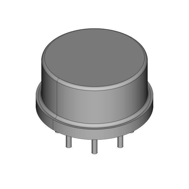
To-99
TOP VIEW
TE
PRODUCT HIGHLIGHTS
°
'
1. Fully gu"ranteed and 100%tested lilV/ C maximum voltage
drift combined with voltage offset of 500IlV (ADS04L).
2. Fully protected input (:!:Vs>and output circuitry. The input
protection circuit prevents offset voltage and bias current
degradation due to reverse breakdown, and is of critical
importance in this type of device whoSe overall performance
is strongly dependent upon front~nd stability. !
3. Single capacitor compensation eliminates elaborate stabilizing networks while providing flexibility not possible with
an internally compensated op amp. This feature allows
bandwidth to be-optimized by the user for his panicular
application.
4. High gain is maintained independent of offset nulling,
power supply voltage and load resistance.
S. Bootstrapping of the critical input transistor quad produces
CMRR and PSRR compatible with the tight IIlVfc drift.
CMRR and PSRR are both in the vicinity of 12OdB.
6. Noise performance is closely monitored at Outgoing QC to
ensure compatibility with the low error budgets afforded by
the performance of all other parameters.
,/
.
7. Eve7. ADS04 receives a stabilization bake for 24 hours at
150 C to ensure reliability and long term stability.
8. The'lOO piece price ofthe ADS04 is 1/3 to 1/2 lesSthan
that of modular low drift operational amplifiers,and is
.
competitive with the price of less accurate IC op amps.
,
�SPECIFICA
JlONS (typical'
PARAMETER
OPEN LOOP GAIN
Vas = :UOV, RL>2kO
T mill
很抱歉,暂时无法提供与“AD504MH”相匹配的价格&库存,您可以联系我们找货
免费人工找货