AD5061YRJZ-1REEL7

AD5061YRJZ-1REEL7

  • 厂商:

    AD(亚德诺)

  • 封装:

    SOT-23-8

  • 描述:

    16-位数模转换器-1-SOT-23-8

  • 详情介绍
  • 数据手册
  • 价格&库存
AD5061YRJZ-1REEL7 数据手册
Data Sheet 16-Bit VOUT, nanoDAC, SPI Interface, 2.7 V to 5.5 V in an SOT-23 AD5061 FEATURES FUNCTIONAL BLOCK DIAGRAM Single 16-bit digital-to-analog converter (DAC), 4 LSB INL Power-on reset to midscale or zero-scale Guaranteed monotonic by design 3 power-down functions Low power serial interface with Schmitt triggered inputs Small 8-lead SOT-23 package, low power Fast settling time of 4 µs typically 2.7 V to 5.5 V power supply Low glitch on power-up SYNC interrupt facility VREF POWER-ON RESET AD5061 BUF OUTPUT BUFFER DAC REGISTER REF(+) VOUT DAC AGND INPUT CONTROL LOGIC POWER-DOWN CONTROL LOGIC RESISTOR NETWORK 04762-001 APPLICATIONS Process control Data acquisition systems Portable battery-powered instruments Digital gain and offset adjustment Programmable voltage and current sources Programmable attenuators SYNC SCLK DACGND DIN Figure 1. GENERAL DESCRIPTION The AD5061, a member of the Analog Devices, Inc., nanoDAC™ family, is a low power, single 16-bit buffered voltage-out DAC that operates from a single 2.7 V to 5.5 V supply. The device offers a relative accuracy specification of ±4 LSB and operation is guaranteed monotonic with a ±1 LSB DNL specification. The device uses a versatile 3-wire serial interface that operates at clock rates up to 30 MHz, and is compatible with standard SPI, QSPI™, MICROWIRE, and DSP interface standards. The reference for the AD5061 is supplied from an external VREF pin. A reference buffer is also provided on-chip. The device incorporates a power-on reset circuit that ensures the DAC output powers up to mid-scale or zero scale and remains there until a valid write takes place to the device. The device contains a power-down feature that reduces the current consumption of the device to typically 330 nA at 5 V and provides software-selectable output loads while in power-down mode. The device is put into powerdown mode over the serial interface. Total unadjusted error for the device is
AD5061YRJZ-1REEL7
物料型号:AD5061

器件简介: - AD5061是Analog Devices公司nanoDAC™系列的一部分,是一款低功耗、单16位缓冲电压输出DAC,工作电压范围为2.7V至5.5V。 - 该设备提供了相对精度规格±4 LSB,并且设计上保证了单调性,具有±1 LSB的DNL规格。
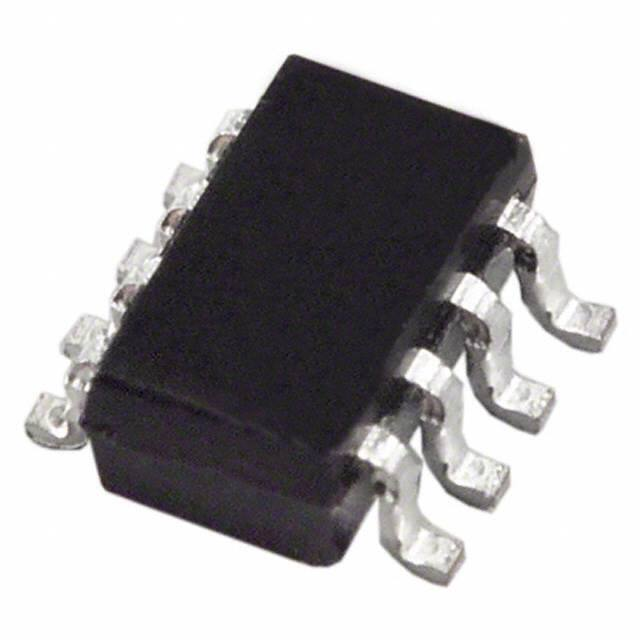
引脚分配: - AD5061采用8引脚SOT-23封装,具体引脚功能如下: - DIN(引脚1):串行数据输入。 - VDD(引脚2):电源输入。 - VREF(引脚3):参考电压输入。 - VOUT(引脚4):DAC的模拟输出电压。 - AGND(引脚5):模拟电路的地参考点。 - DACGND(引脚6):DAC的地输入。 - SYNC(引脚7):电平触发的控制输入(活跃低)。 - SCLK(引脚8):串行时钟输入。

参数特性: - 16位分辨率,4 LSB的积分非线性(INL)。 - 电源电压范围2.7V至5.5V。 - 低功耗,典型快速建立时间4微秒。 - 低上电时的抖动。 - 高速串行接口,时钟速度高达30MHz。 - 三种软件可选的电源关闭模式。

功能详解: - AD5061具有电源开启复位功能,可将DAC输出设置为中尺度或零尺度,并保持该状态直到设备进行有效写入。 - 设备包含电源关闭特性,可将电流消耗降低至典型值330 nA(5V供电时)。 - 通过串行接口进入电源关闭模式。

应用信息: - 过程控制、数据采集系统、便携式电池供电仪器、数字增益和偏移调整、可编程电压和电流源、可编程衰减器等。

封装信息: - AD5061采用小型8引脚SOT-23封装,具有低功耗特点。
AD5061YRJZ-1REEL7 价格&库存

很抱歉,暂时无法提供与“AD5061YRJZ-1REEL7”相匹配的价格&库存,您可以联系我们找货

免费人工找货