0
登录后你可以
  • 下载海量资料
  • 学习在线课程
  • 观看技术视频
  • 写文章/发帖/加入社区
会员中心
创作中心
发布
  • 发文章

  • 发资料

  • 发帖

  • 提问

  • 发视频

创作活动
AD5062BRJZ-1500RL7

AD5062BRJZ-1500RL7

  • 厂商:

    AD(亚德诺)

  • 封装:

    SOT-23-8

  • 描述:

    AD5062 - FULLY ACCURATE 16 BIT V

  • 详情介绍
  • 数据手册
  • 价格&库存
AD5062BRJZ-1500RL7 数据手册
Fully Accurate 16-Bit VOUT nanoDAC™ SPI Interface 2.7 V to 5.5 V, in an SOT-23 AD5062 FEATURES FUNCTIONAL BLOCK DIAGRAM VREF Single 16-bit DAC, 1 LSB INL Power-on reset to midscale or zero-scale Guaranteed monotonic by design 3 power-down functions Low power serial interface with Schmitt-triggered inputs Tiny 8-lead SOT-23 package, low power Fast settling time of 4 μs typically 2.7 V to 5.5 V power supply Low glitch on power-up Unbuffered voltage capable of driving 60 kΩ load SYNC interrupt facility POWER-ON RESET DAC REGISTER BUF VDD AD5062 REF(+) VOUT DAC AGND INPUT CONTROL LOGIC RESISTOR NETWORK 04766-001 POWER-DOWN CONTROL LOGIC APPLICATIONS Process control Data acquisition systems Portable battery-powered instruments Digital gain and offset adjustment Programmable voltage and current sources Programmable attenuators SYNC SCLK DIN DACGND Figure 1. Table 1. Related Devices Part No. AD5061 AD5063 AD5040/AD5060 Description 2.7 V to 5.5 V, 16-bit nanoDAC D/A, 4 LSBs INL, SOT-23. 2.7 V to 5.5 V, 16-bit nanoDAC D/A, 1 LSB INL, MSOP. 2.7 V to 5.5 V, 14-/16-bit nanoDAC D/A, 1 LSB INL, SOT-23. GENERAL DESCRIPTION PRODUCT HIGHLIGHTS The AD5062, a member of ADI’s nanoDAC family, is a low power, single 16-bit unbuffered voltage-out DAC that operates from a single 2.7 V to 5.5 V supply. The part offers a relative accuracy specification of ±1 LSB, and operation is guaranteed monotonic with a ±1 LSB DNL specification. The part uses a versatile 3-wire serial interface that operates at clock rates up to 30 MHz, and is compatible with standard SPI®, QSPI™, MICROWIRE™, and DSP interface standards. The reference for the AD5062 is supplied from an external VREF pin. A reference buffer is also provided on-chip. The part incorporates a poweron reset circuit that ensures the DAC output powers up to zero scale or mid-scale and remains there until a valid write takes place to the device. The part contains a power-down feature that reduces the current consumption of the device to typically 300 nA at 5 V and provides software-selectable output loads while in power-down mode. The part is put into power-down mode over the serial interface. Total unadjusted error for the part is
AD5062BRJZ-1500RL7
物料型号:AD5062 器件简介:AD5062是Analog Devices公司生产的一款低功耗、单16位非缓冲电压输出DAC,工作电压范围为2.7V至5.5V。

它具有高精度输出(±1LSB相对精度)、保证单调性、快速的SPI接口(时钟频率高达30MHz),并且提供上电复位至中量程或零量程以及多种省电模式。

引脚分配: 1. DIN - 串行数据输入 2. VDD - 电源输入 3. VREF - 参考电压输入 4. VOUT - DAC模拟输出电压 5. AGND - 模拟电路接地参考点 6. DACGND - DAC接地输入 7. SYNC - 控制输入(低电平有效),用于输入数据同步 8. SCLK - 串行时钟输入 参数特性: - 分辨率:16位 - 相对精度(INL):最高±1LSB - 总未校正误差(TUE):最高±0.8mV - 差分非线性(DNL):±1LSB,保证单调性 - 增益误差:最高±0.02%FSR - 偏移误差:最高±0.05mV - 输出电压范围:0至VREF - 输出电压建立时间:典型值4μs - 电源电压范围:2.7V至5.5V - 功耗:典型值0.65mA(正常模式) 功能详解: AD5062通过SPI接口接收24位数据,其中最高2位用于控制电源模式,中间16位为DAC数据输入。

它包含上电复位电路,可以在上电时输出中量程或零量程,还具备省电模式,减少功耗至300nA。

此外,AD5062支持软件复位和快速建立时间,适用于高速应用。

应用信息: - 过程控制 - 数据采集系统 - 便携式电池供电仪器 - 数字增益和偏移调整 - 可编程电压和电流源 - 可编程衰减器 
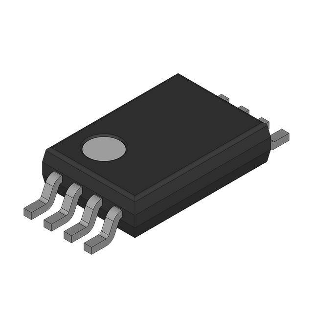
封装信息:AD5062采用8引脚SOT-23小型封装。
AD5062BRJZ-1500RL7 价格&库存

很抱歉,暂时无法提供与“AD5062BRJZ-1500RL7”相匹配的价格&库存,您可以联系我们找货

免费人工找货
AD5062BRJZ-1500RL7
  •  国内价格
  • 1+140.09760
  • 10+133.28280
  • 30+121.48920
  • 100+108.97287

库存:3