Quad Channel, 256-Position, SPI,
Nonvolatile Digital Potentiometer
AD5144-EP
Enhanced Product
FEATURES
FUNCTIONAL BLOCK DIAGRAM
10 kΩ resistance option
Resistor tolerance: 8% maximum
Maximum continuous current: ±6 mA at RAB = 10 kΩ
Low resistance temperature coefficient: 35 ppm/°C typical
Wide bandwidth: 3 MHz at RAB = 10 kΩ
Fast start-up time: 75 µs
Linear gain setting mode
Single- and dual-supply operation
Independent VLOGIC: 1.8 V to 5.5 V
VLOGIC
ENHANCED PRODUCT FEATURES
VDD
AD5144-EP
POWER-ON
RESET
RDAC1
A1
INPUT
REGISTER 1
W1
B1
RDAC2
SYNC
SCLK
SDI
INPUT
REGISTER 2
SPI
SERIAL
INTERFACE
B2
RDAC3
7/8
INPUT
REGISTER 3
SDO
A3
W3
B3
RDAC4
A4
INPUT
REGISTER 4
W4
B4
EEPROM
MEMORY
GND
21593-001
Supports defense and aerospace applications
(AQEC standard)
Military temperature range: −55°C to +125°C
Controlled manufacturing baseline
One assembly/test site
One fabrication site
Product change notification
Qualification data available on request
A2
W2
VSS
Figure 1.
APPLICATIONS
Missiles and munitions
Avionics and unmanned systems
Programmable filters, delays, and time constants
Programmable power supplies
GENERAL DESCRIPTION
The AD5144-EP potentiometer provides a nonvolatile solution
for 256-position adjustment applications, offering guaranteed low
resistor tolerance errors of ±8% and up to ±6 mA current density
in the Ax, Bx, and Wx pins.
The low wiper resistance of 40 Ω at the ends of the resistor array
allow for pin-to-pin connection.
The low resistor tolerance and low nominal temperature
coefficient simplify open-loop applications as well as
applications requiring tolerance matching.
The wiper values can be set through a serial peripheral interface
(SPI) digital interface that is also used to read back the wiper
register and electronically erasable programmable read-only
memory (EEPROM) contents.
The linear gain setting mode allows independent programming
of the resistance between the digital potentiometer terminals,
through the Terminal A to Terminal W (RAW) and the Terminal W
to Terminal B (RWB) string resistors, allowing accurate resistor
matching.
Additional application and technical information can be found
in the AD5144 data sheet.
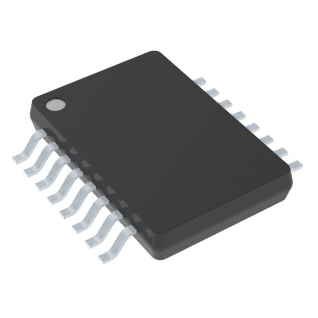
The AD5144-EP is available in a 20-lead TSSOP. The device is
guaranteed to operate over the −55°C to +125°C temperature
range.
The high bandwidth and low total harmonic distortion (THD)
ensure optimal performance for ac signals, making this device
suitable for filter design.
Rev. A
Document Feedback
Information furnished by Analog Devices is believed to be accurate and reliable. However, no
responsibility is assumed by Analog Devices for its use, nor for any infringements of patents or other
rights of third parties that may result from its use. Specifications subject to change without notice. No
license is granted by implication or otherwise under any patent or patent rights of Analog Devices.
Trademarks and registered trademarks are the property of their respective owners.
One Technology Way, P.O. Box 9106, Norwood, MA 02062-9106, U.S.A.
Tel: 781.329.4700
©2019 Analog Devices, Inc. All rights reserved.
Technical Support
www.analog.com
�AD5144-EP
Enhanced Product
TABLE OF CONTENTS
Features .............................................................................................. 1
Shift Register and Timing Diagrams ..........................................5
Enhanced Product Features ............................................................ 1
Absolute Maximum Ratings ............................................................7
Applications ....................................................................................... 1
Thermal Resistance .......................................................................7
General Description ......................................................................... 1
ESD Caution...................................................................................7
Functional Block Diagram .............................................................. 1
Pin Configuration and Function Descriptions..............................8
Revision History ............................................................................... 2
Typical Performance Characteristics ..............................................9
Specifications..................................................................................... 3
Outline Dimensions ....................................................................... 11
Electrical Characteristics ............................................................. 3
Ordering Guide .......................................................................... 11
Interface Timing Specifications .................................................. 5
REVISION HISTORY
10/2019—Rev. 0 to Rev. A
Changes to Table 1 ............................................................................ 4
9/2019—Revision 0: Initial Version
Rev. A | Page 2 of 11
�Enhanced Product
AD5144-EP
SPECIFICATIONS
ELECTRICAL CHARACTERISTICS
VDD = 2.3 V to 5.5 V and VSS = 0 V for the single-supply range, VDD = 2.25 V to 2.75 V and VSS = −2.25 V to −2.75 V for the dual-supply
range, VLOGIC = 1.8 V to 5.5 V, and −55°C < TA < +125°C, unless otherwise noted. See the AD5144 data sheet for the test circuits that
define the test conditions used in the Specifications section.
Table 1.
Parameter
DC CHARACTERISTICS—RHEOSTAT
MODE (ALL RESISTIVE DIGITAL-TOANALOG CONVERTERS (RDACs))
Resolution
Resistor Integral Nonlinearity 2
Resistor Differential Nonlinearity2
Nominal Resistor Tolerance
Resistance Temperature Coefficient3
Wiper Resistance3
Bottom Scale or Top Scale
Nominal Resistance Match
DC CHARACTERISTICS—POTENTIOMETER
DIVIDER MODE (ALL RDACs)
Integral Nonlinearity 4
Differential Nonlinearity4
Full-Scale Error
Zero-Scale Error
Voltage Divider Temperature
Coefficient3
RESISTOR TERMINALS
Maximum Continuous Current
Symbol
Test Conditions/Comments
N
R-INL
INL
DNL
VWFSE
VWZSE
(ΔVW/VW)/ΔT × 106
Code = full scale
Code = zero scale, RAB = 10 kΩ
RAB = 10 kΩ
Code = 0xFF
RAB = 10 kΩ
RAB = 10 kΩ
RAB = 10 kΩ
Code = half scale
Max
−2
−5
−0.5
−8
−1
−1
−0.5
−2.5
Unit
Bits
±0.2
±1.5
±0.2
±1
35
55
40
±0.2
+2
+5
+0.5
+8
±0.2
±0.2
−0.1
1.2
±5
+1
+0.5
125
80
+1
3
LSB
LSB
LSB
%
ppm/°C
Ω
Ω
%
LSB
LSB
LSB
LSB
ppm/°C
IA, IB, and IW
RAB = 10 kΩ
CA, CB
Capacitance W3
CW
Common-Mode Leakage Current3
Low
Input Hysteresis3
Input Current3
Input Capacitance3
Typ 1
8
Terminal A and Terminal B
resistor (RAB) = 10 kΩ
VDD ≥ 2.7 V
VDD < 2.7 V
R-DNL
ΔRAB/RAB
(ΔRAB/RAB)/ΔT × 106
RW
RBS or RTS
RAB1/RAB2
Terminal Voltage Range 5
Capacitance A, Capacitance B3
DIGITAL INPUTS
Input Logic3
High
Min
VINH
f = 1 MHz, measured to GND,
code = half scale, RAB = 10 kΩ
f = 1 MHz, measured to GND,
code = half scale, RAB = 10 kΩ
Terminal A voltage (VA) =
wiper terminal voltage (VW) =
Terminal B voltage (VB)
VLOGIC = 1.8 V to 2.3 V
VLOGIC = 2.3 V to 5.5 V
VINL
VHYST
IIN
CIN
−6
VSS
−500
+6
VDD
25
mA
V
pF
12
pF
±15
+500
0.8 × VLOGIC
0.7 × VLOGIC
0.2 × VLOGIC
0.1 × VLOGIC
±1
5
Rev. A | Page 3 of 11
nA
V
V
V
V
µA
pF
�AD5144-EP
Parameter
DIGITAL OUTPUTS
Output High Voltage3
Output Low Voltage3
Enhanced Product
Symbol
Test Conditions/Comments
VOH
Pull-up resistor (RPULL-UP) =
2.2 kΩ to VLOGIC
Sink current (ISINK) = 3 mA
ISINK = 6 mA, VLOGIC > 2.3 V
VOL
Three-State Leakage Current
Three-State Output Capacitance
POWER SUPPLIES
Single-Supply Range
Dual-Supply Range
Logic Supply Range
Positive Supply Current
Negative Supply Current
EEPROM Store Current3, 6
EEPROM Read Current3, 7
Logic Supply Current
Power Dissipation 8
Power Supply Rejection Ratio
DYNAMIC CHARACTERISTICS 9
Bandwidth
Total Harmonic Distortion
Min
Typ 1
Max
VLOGIC
−1
V
0.4
0.6
+1
V
V
µA
pF
5.5
±2.75
VDD
VDD
V
V
V
V
5.5
µA
nA
µA
mA
µA
µA
µW
dB
2
VSS = GND
IDD
ISS
IDD_EEPROM_STORE
IDD_EEPROM_READ
ILOGIC
PDISS
PSRR
BW
THD
Resistor Noise Density
eN_WB
VW Settling Time
tS
Crosstalk (CW1/CW2)
Analog Crosstalk
Endurance 10
CT
CTA
Single supply, VSS = GND
Dual supply, VSS < GND
VINH = VLOGIC or VINL = GND
VDD = 5.5 V
VDD = 2.3 V
VINH = VLOGIC or VINL = GND
VINH = VLOGIC or VINL = GND
VINH = VLOGIC or VINL = GND
VINH = VLOGIC or VINL = GND
VINH = VLOGIC or VINL = GND
ΔVDD/ΔVSS = VDD ± 10%,
code = full scale
2.3
±2.25
1.8
2.25
−5.5
−3 dB, RAB = 10 kΩ
VDD/VSS = ±2.5 V, VA = 1 V rms,
VB = 0 V, f = 1 kHz
Code = half scale, TA = 25°C,
f = 10 kHz, RAB = 10 kΩ
VA = 5 V, VB = 0 V, from zero
scale to full scale, ±0.5 LSB
error band, RAB = 10 kΩ
RAB = 10 kΩ
TA = 25°C
−40°C < TA < +125°C
Data Retention 11, 12
0.7
400
−0.7
2
320
0.05
3.5
−66
Unit
1.4
−60
3
−80
MHz
dB
7
nV/√Hz
2
µs
10
−90
1
nV-sec
dB
Mcycles
kcycles
Years
100
50
Typical values represent average readings at 25°C, VDD = 5 V, VSS = 0 V, and VLOGIC = 5 V.
Resistor integral nonlinearity error (R-INL) is the deviation from an ideal value measured between the maximum resistance and the minimum resistance wiper
positions. R-DNL measures the relative step change from ideal between successive tap positions. The maximum wiper current is limited to (0.7 × VDD)/RAB.
3
Guaranteed by design and characterization, not subject to production test.
4
INL and DNL are measured across the Terminal W and Terminal B voltage (VWB) with the RDAC configured as a potentiometer divider similar to a voltage output DAC.
VA = VDD and VB = 0 V. DNL specification limits of ±1 LSB maximum are guaranteed monotonic operating conditions.
5
Resistor Terminal A, Resistor Terminal B, and Resistor Terminal W have no limitations on polarity with respect to each other. Dual-supply operation enables ground
referenced bipolar signal adjustment.
6
IDD_EEPROM_STORE is different from the operating current. Supply current for EEPROM program lasts approximately 30 ms.
7
IDD_EEPROM_READ is different from the operating current. Supply current for EEPROM read lasts approximately 20 µs.
8
PDISS is calculated from (IDD × VDD) + (ILOGIC × VLOGIC).
9
All dynamic characteristics use VDD/VSS = ±2.5 V, and VLOGIC = 2.5 V.
10
Endurance is qualified per JEDEC Standard 22, Method A117 to 100,000 cycles measured at −40°C to +125°C.
11
Retention lifetime equivalent at junction temperature (TJ) = 125°C per JEDEC Standard 22, Method A117. Retention lifetime based on an activation energy of 1 eV,
derates with junction temperature in the Flash/EE memory.
12
50 years apply to an endurance of 1000 cycles. An endurance of 100,000 cycles has an equivalent retention lifetime of 5 years.
1
2
Rev. A | Page 4 of 11
�Enhanced Product
AD5144-EP
INTERFACE TIMING SPECIFICATIONS
VLOGIC = 1.8 V to 5.5 V, and all specifications TMIN to TMAX, unless otherwise noted.
Table 2. SPI Interface
Parameter 1
t1
Test Conditions/Comments
VLOGIC > 1.8 V
VLOGIC = 1.8 V
VLOGIC > 1.8 V
VLOGIC = 1.8 V
VLOGIC > 1.8 V
VLOGIC = 1.8 V
t2
t3
Min
20
30
10
15
10
15
10
5
5
10
20
t4
t5
t6
t7
t8 2
t9 3
t10
tPOWER-UP
Typ
Max
50
500
75
Unit
ns
ns
ns
ns
ns
ns
ns
ns
ns
ns
ns
ns
ns
µs
Description
SCLK cycle time
SCLK high time
SCLK low time
SYNC to SCLK falling edge setup time
Data setup time
Data hold time
SYNC rising edge to next SCLK fall ignored
Minimum SYNC high time
SCLK rising edge to SDO valid
SYNC rising edge to SDO pin disable
Start-up time (not shown in Figure 3 and Figure 4)
All input signals are specified with rising time (tR) = falling time (tF) = 1 ns/V (10% to 90% of VDD) and timed from a voltage level of (VIL + VIH)/2.
Refer to tEEPROM_PROGRAM and tEEPROM_READBACK for memory command operations (see the control pins table in the AD5144 data sheet for additional information).
3
The pull-up resistance (RPULL_UP) = 2.2 kΩ to VDD with a capacitance load of 168 pF.
1
2
SHIFT REGISTER AND TIMING DIAGRAMS
C3
C2
C1
C0
A2
A3
A1
DB8
DB7
A0
D7
DB0 (LSB)
D6
D5
D4
D3
D2
D0
D1
21593-002
DB15 (MSB)
DATA BITS
ADDRESS BITS
CONTROL BITS
Figure 2. Input Shift Register Contents
t4
t1
t2
t7
SCLK
t3
t8
SYNC
t5
t6
C3
C2
C1
C0
D7
D6
D5
SDO
C3*
C2*
C1*
C0*
D7*
D6*
D5*
D2
D1
D0
D2*
D1*
D0*
t9
t10
*PREVIOUS COMMAND RECEIVED.
Figure 3. SPI Serial Interface Timing Diagram, CPOL = 0, CPHA = 1
Rev. A | Page 5 of 11
21593-003
SDI
�AD5144-EP
Enhanced Product
t4
t1
t2
t7
SCLK
t3
t8
SYNC
t5
t6
C3
C2
C1
C0
D7
D6
D5
SDO
C3*
C2*
C1*
C0*
D7*
D6*
D5*
D2
D1
D0
D2*
D1*
D0*
t9
t10
*PREVIOUS COMMAND RECEIVED.
Figure 4. SPI Serial Interface Timing Diagram, CPOL = 1, CPHA = 0
Rev. A | Page 6 of 11
21593-004
SDI
�Enhanced Product
AD5144-EP
ABSOLUTE MAXIMUM RATINGS
TA = 25°C, unless otherwise noted.
Table 3.
Parameter
VDD to GND
VSS to GND
VDD to VSS
VLOGIC to GND
VA, VW, VB to GND
IA, IW, IB
Pulsed 1, RAW = 10 kΩ
Frequency > 10 kHz
Frequency ≤ 10 kHz
Digital Inputs
Operating Temperature Range, TA 3
Maximum Junction Temperature,
TJ Maximum
Storage Temperature Range
Reflow Soldering
Peak Temperature
Time at Peak Temperature
Package Power Dissipation
Field Induced Charged Device Model
(FICDM)
Rating
−0.3 V to +7.0 V
+0.3 V to −7.0 V
7V
−0.3 V to VDD + 0.3 V or
+7.0 V (whichever is less)
VSS − 0.3 V, VDD + 0.3 V
±6 mA/d 2
±6 mA/√d2
−0.3 V to VLOGIC + 0.3 V or
+7 V (whichever is less)
−55°C to +125°C
150°C
Stresses at or above those listed under Absolute Maximum
Ratings may cause permanent damage to the product. This is a
stress rating only; functional operation of the product at these
or any other conditions above those indicated in the operational
section of this specification is not implied. Operation beyond
the maximum operating conditions for extended periods may
affect product reliability.
THERMAL RESISTANCE
Thermal performance is directly linked to printed circuit board
(PCB) design and operating environment. Careful attention to
PCB thermal design is required.
θJA is the natural convection, junction to ambient thermal
resistance measured in a one cubic foot sealed enclosure, and
θJC is the junction to case thermal resistance measured at
package top.
Table 4. Thermal Resistance
Package Type
RU-20
−65°C to +150°C
1
260°C
20 sec to 40 sec
(TJ max − TA)/θJA
1.5 kV
θJA1
143
θJC
45
Unit
°C/W
Thermal impedance simulated values are based on a JEDEC 2S2P thermal
test board, still air (0 m/sec airflow). See JEDEC JESD-51.
ESD CAUTION
The maximum terminal current is bounded by the maximum current
handling of the switches, the maximum power dissipation of the package,
and the maximum applied voltage across any two of the A, B, and W
terminals at a given resistance.
2
d = pulse duty factor.
3
TA includes programming of EEPROM memory.
1
Rev. A | Page 7 of 11
�AD5144-EP
Enhanced Product
PIN CONFIGURATION AND FUNCTION DESCRIPTIONS
SYNC
1
20
SDO
GND
2
19
SDI
A1
3
18
SCLK
W1
4
17
VLOGIC
B1
5
A3
6
AD5144-EP
VDD
TOP VIEW
(Not to Scale) 15 B4
16
7
14
B3
8
13
A4
VSS
9
12
B2
A2 10
11
W2
21593-005
W4
W3
Figure 5. Pin Configuration
Table 5. Pin Function Descriptions
Pin No.
1
2
3
4
5
6
7
8
9
10
11
12
13
14
15
16
17
18
19
20
Mnemonic
SYNC
GND
A1
W1
B1
A3
W3
B3
VSS
A2
W2
B2
A4
W4
B4
VDD
VLOGIC
SCLK
SDI
SDO
Description
Synchronization Data Input, Active Low. When SYNC returns high, data is loaded into the input shift register.
Ground Pin, Logic Ground Reference.
Terminal A of RDAC 1. VSS ≤ VA ≤ VDD.
Wiper Terminal of RDAC 1. VSS ≤ VW ≤ VDD.
Terminal B of RDAC 1. VSS ≤ VB ≤ VDD.
Terminal A of RDAC 3. VSS ≤ VA ≤ VDD.
Wiper Terminal of RDAC 3. VSS ≤ VW ≤ VDD.
Terminal B of RDAC 3. VSS ≤ VB ≤ VDD.
Negative Power Supply. Decouple this pin with 0.1 µF ceramic capacitors and 10 µF capacitors.
Terminal A of RDAC 2. VSS ≤ VA ≤ VDD.
Wiper Terminal of RDAC 2. VSS ≤ VW ≤ VDD.
Terminal B of RDAC 2. VSS ≤ VB ≤ VDD.
Terminal A of RDAC 4. VSS ≤ VA ≤ VDD.
Wiper Terminal of RDAC 4. VSS ≤ VW ≤ VDD.
Terminal B of RDAC 4. VSS ≤ VB ≤ VDD.
Positive Power Supply. Decouple this pin with 0.1 µF ceramic capacitors and 10 µF capacitors.
Logic Power Supply, 1.8 V to VDD. Decouple this pin with 0.1 µF ceramic capacitors and 10 µF capacitors.
Serial Clock Line. Data is clocked in at the logic low transition.
Serial Data Input.
Serial Data Output. SDO is an open-drain output pin that must have an external pull-up resistor.
Rev. A | Page 8 of 11
�Enhanced Product
AD5144-EP
TYPICAL PERFORMANCE CHARACTERISTICS
0.3
0.2
+125°C
+25°C
–55°C
+125°C
+25°C
–55°C
0.2
0.1
R-DNL (LSB)
R-INL (LSB)
0.1
0
0
–0.1
–0.1
0
15
30
45
60
75
90 105 120 135 150 165 180 195 210 225 240 255
CODE (Decimal)
–0.3
21593-006
–0.3
0
15
30
45
60
75
90 105 120 135 150 165 180 195 210 225 240 255
CODE (Decimal)
Figure 6. R-INL vs. Code for Various Temperatures
21593-009
–0.2
–0.2
Figure 9. R-DNL vs. Code for Various Temperatures
0.3
0.10
+125°C
+25°C
–55°C
0.05
0.2
0
DNL (LSB)
INL (LSB)
0.1
0
–0.05
–0.10
–0.15
–0.1
–0.20
0
15
30
45
60
75
90 105 120 135 150 165 180 195 210 225 240 255
CODE (Decimal)
0
15
30
45
60
75
90 105 120 135 150 165 180 195 210 225 240 255
CODE (Decimal)
Figure 7. INL vs. Code for Various Temperatures
Figure 10. DNL vs. Code for Various Temperatures
1600
1400
+125°C
+25°C
–55°C
–0.30
21593-007
–0.3
–0.25
21593-010
–0.2
100
VDD = 2.3V
VDD = 3.4V
VDD = 5.5V
80
VLOGIC = 2.3V
VLOGIC = 3.4V
VLOGIC = 5.5V
1200
ILOGIC (nA)
IDD (nA)
1000
800
600
60
40
400
20
5
20
35
50
65
TEMPERATURE (°C)
80
95
110 125
0
–55 –40 –25 –10
21593-008
0
–55 –40 –25 –10
5
20
35
50
65
80
95
110 125
TEMPERATURE (°C)
Figure 8. Supply Current (IDD) vs. Temperature for Various Power Supplies
Rev. A | Page 9 of 11
Figure 11. ILOGIC vs Temperature for Various Logic Voltages
21593-011
200
�Enhanced Product
450
400
400
350
300
250
200
150
100
50
350
300
250
200
150
100
50
0
0
–50
–50
0
50
100
150
CODE (DECIMAL)
200
255
Figure 12. Potentiometer Mode Temperature Coefficient ((ΔVW/VW)/ΔT × 106)
vs. Code
0
50
100
150
CODE (DECIMAL)
200
255
21593-013
RHEOSTAT MODE TEMPERATURE
COEFFICIENT (ppm/°C)
450
21593-012
POTENTIOMETER MODE TEMPERATURE
COEFFICIENT (ppm/°C)
AD5144-EP
Figure 13. Rheostat Mode Temperature Coefficient ((ΔRWB/RWB)/ΔT × 106) vs.
Code
Rev. A | Page 10 of 11
�Enhanced Product
AD5144-EP
OUTLINE DIMENSIONS
6.60
6.50
6.40
20
11
4.50
4.40
4.30
6.40 BSC
1
10
PIN 1
0.65
BSC
1.20 MAX
0.15
0.05
COPLANARITY
0.10
0.30
0.19
0.20
0.09
SEATING
PLANE
0.75
0.60
0.45
8°
0°
COMPLIANT TO JEDEC STANDARDS MO-153-AC
Figure 14. 20-Lead Thin Shrink Small Outline Package [TSSOP]
(RU-20)
Dimensions shown in millimeters
ORDERING GUIDE
Model 1
AD5144TRUZ10-EP
AD5144TRUZ10-EP-R7
1
RAB (kΩ)
10
10
Resolution
256
256
Interface
SPI
SPI
Temperature Range
−55°C to +125°C
−55°C to +125°C
Z = RoHS Compliant Part.
©2019 Analog Devices, Inc. All rights reserved. Trademarks and
registered trademarks are the property of their respective owners.
D21593-0-10/19(A)
Rev. A | Page 11 of 11
Package Description
20-Lead TSSOP
20-Lead TSSOP
Package Option
RU-20
RU-20
�