256-Position SPI Compatible
Dual Digital Potentiometer
AD5162
Evaluation Board User Manual
5 Steps To Setup The Evaluation Board…
1.
Install AD5162 Software
3. Open AD5162 RevA.exe
4. Provide Power SupplyOr Use
Power from Parallel Port
+5V
GND
W
2. Configure Board and Connect to Parallel Port with
Provided Parallel Cable
B
5. Measure Result
Figure 1. Evaluation Kit Setup
No Programming
Skills Required!
Rev B 11/03/03
1
�256-Position SPI Compatible
Dual Digital Potentiometer
AD5162
Evaluation Board User Manual
General Overview
This evaluation board provides the user with a simple and quick solution to evaluate digital potentiometers from
Analog Devices. Only one digital pot can be placed on the board at a time. For the user’s convenience, a general
purpose opamp, 2.5V voltage reference, and two power MOSFETs are included and can be configured in a variety of
flexible configurations. The digital pot can be used by itself or in conjunction with these other components.
How to Get Started
1.
Click on the Install Software link in the Digital POT CD browser or setup.exe if you don’t have the CD browser.
2.
Configure board to your liking(refer to “Configuring Other Components” on page 4 for more details). A two
channel opamp(AD822B), 2.5V reference(ADR03), and two power mosfets(FDV301N) are provided for your
convenience. If you would simply like to evaluate the digital pot, then ignore Step 2 and proceed to Step 3.
3.
Apply a separate power supply or use power from the parallel port(refer to “Powering the AD5162” on page 4 to
avoid damaging the part).
4.
Connect board to parallel port with provided parallel cable.
5.
Open the AD5162 Rev A program from the Windows Start – Program. Move scroll bar to program resistance
settings. The operation is self-explanatory.
Figure 2. AD5162 Software Graphic al Interface
Rev B 11/03/03
2
�256-Position SPI Compatible
Dual Digital Potentiometer
AD5162
Evaluation Board User Manual
1
2
3
U5
U12
ADR03 2.5V Reference
1
2
3
VDD
C2
5
Temp Trim
GND
Vin Vout
4
AGND
C
8 A1
7 B1
6 CS/AD0
5 SDI/SDA
A
B
CS
SDI
A1
1
2
B1
CS/AD0 3
SDO 4
SDI/SDA5
A
B
CS/AD0
SDO/NC
SDI/SDA
VDD 1
DGND 2
CLK/SCL
3
VDD
GND
SCL
6 B1
5 W1
4 SDI/SDA
B
W
SDA
W1
1
VDD 2
DGND 3
CLK/SCL
4
W
VDD
GND
SCL
A
B
AD0
SDA
8 A1
7 B1
6 CS/AD0
5 SDI/SDA
AD5245
SDO
1
U14
B1
1
A1
A1
2
W1
W1
3
B3
B3
4
A3
A3
5
W3
W3
6
VDD
7
DGND
8
10
W1
9 B2
8 RES/AD1
7 SDI/SDA
6 CLK/SCL
W1
B2
AD1
SDA
SCL
W1
10
9 VDD
8 DIS
7 DGND
6 CLK/SCL
W
VDD
SPI/I2C
GND
CLK/SCL
A1
2
W1
3
B1
4
24 B2
B2
VDD
5
23 A2
A2
SHDN
6
22 W2
W2
CLK/SCL 7
21 B4
B4
SDI/SDA 8
20 A4
A4
19 W4
W4
U2
U1
JP4
B1
AD0
W2
GND
VDD
U6
AD5246
B1
AD5243
B1
1
CS/AD0 2
W2
3
DGND 4
VDD 5
W
VDD
GND
CLK
AD5161
10W1
9 B2
8 A2
7 SDI/SDA
6 CLK/SCL
W1
B2
A2
SDA
SCL
W1
1
VDD 2
DGND 3
CLK/SCL
4
AD5160
JP5
B1
A1
W2
GND
VDD
U9
U7
6 A1
5 W1
4 SDI/SDA
A
W
SDA
U8
U10
1
2
3
4
5
VDD
GND
SCL
C3
0.1u
D
B1
A1
W2
DGND
VDD
VDD 1
DGND 2
CLK/SCL
3
AD5247
ADR03
0.1u
VREF
5
4
AD5248
DIS
9
VL
10
SDI/SDA 11
VDD
CLK/SCL 12
VDD
B1
B2
A1
A2
W1
W2
B3
B4
A3
A4
W3
W4
VDD
VSS
GND
NC/O2
DIS
SDO/O1
VLOGIC
SHDN
SDI/SDA
RESB/AD1
CLK/SCL
CS/AD0
O1
A2
A1
W2
W1
B2
B1
VL
VDD
VSS
SHDN
GND
SCL
AD1
SDA
AD0
16 A2
15 W2
14 B2
13 VL
12 VSS
11 DGND
10 RES/AD1
9
CS/AD0
AD5282
JP2
18 VSS
17 NC/O2 O2
16 SDO
C16
C17
0.1u
10u
JP3
B1
A1
W2
DGND
VDD
VSS
1
2
3
4
5
15 SHDN
U11
B1
A1
W2
GND
VDD
W1
B2
CS
SDI
CLK
10W1
9 B2
8 CS/AD0
7 SDI/SDA
6 CLK/SCL
AD5162
14 RES/AD1
13 CS/AD0
OUT1
1
-IN1
2
U13
OUT1
V+
8
V+
7
OUT2
6
-IN2
5
+IN2
AD5263
-IN1
OUT2
U3A
JP1
+IN1
3
V-
4
+IN1
J1
13
25
12
24
11
23
10
22
9
21
8
20
7
19
6
18
5
17
4
16
3
15
2
14
1
B
DGNDPAD
DGND
C1
10u
R10
10k
R11
10k
R12
10k
R13
10k
R14
10k
R15
10k
R16
10k
U3
SDO
1
A1
2
W1
3
B1
4
100
VDD
5
100
SHDN
6
SDO/O1
470
R8
R6
R5
R4
R3
R2
R1
U3B
+IN2
AD822
R9
R7
V-
-IN2
AD822 Dual Opamp
SHDN
DIS
FDV301N Power FETs
CLK/SCL 7
100
RES/AD1
100
D1
SDI/SDA 8
D2
CS/AD0
W2
W1
B1
VDD
SHDN
B2
VL
VSS
GND
CLK
PR
SDI
CS
16 A2
15 W2
14 B2
13 VL
12 VSS
11 DGND
10 VDD
9
CS/AD0
CLK/SCL
100
220
220
SDI/SDA
VDD
W1
CP15
CP17
Q1
FDV301 W2
JP14
JP15
Q2
FDV301
A
CP16
C5
0.1u
A2
A1
AD5262
100
DB25
C4
0.1u
SDO
C6
0.1u
C7
0.1u
C8
0.1u
C9
0.1u
C10
0.1u
C11
0.1u
C12
0.1u
C13
0.1u
C14
0.1u
CP18
SDO
1
A1
2
W1
3
B1
4
VDD
5
SHDN
6
CLK/SCL 7
C15
0.1u
SDI/SDA 8
U4
O1
A2
A1
W2
W1
B1
VDD
B2
O2
VSS
SHDN
GND
SCL
AD1
SDA
AD0
16 A2
15 W2
14 B2
13 NC/O2
12 VSS
11 DGND
10 RES/AD1
9
CS/AD0
AD5242
1
2
3
Figure 3. Evaluation Board Schematic
Rev B 11/03/03
3
4
5
�256-Position SPI Compatible
Dual Digital Potentiometer
AD5162
Evaluation Board User Manual
JP7
VCC
JP6
VDD
C18
0.1u
V+
C19
10u
CP8
CP1
CP3
-IN1
CP2
JP10
Vin1
2
CP4
JP13
U3A
+IN13
1
+IN25
OUT1
4
CP6
CP11
6
JP12
Vin2
8
JP11
CP10
-IN2
CP9
7
U3B
OUT2
CP13 CP14
CP12
CP7
CP5
VJP8
JP9
C20
C21
0.1u
10u
VEE
Opamp configuration
Figure 4. Detailed Opamp Connections
Powering the AD5162: Two Options for Powering
I. Using the power from the parallel port as VDD
Simply connect JP1.
The voltage level will be whatever your parallel port operates at.
II. Using a separate supply
DO NOT connect JP1.
Connect voltage supply power and ground to the VDD and GND pads on the board.
Configuring other Components
Two Channel Opamp - AD822
Positive Supply
To use the same VDD as the AD5162, connect JP6.
To use a separate positive supply, connect JP7 and apply positive supply(no more than +15V) to the VCC
pad.
Negative Supply
To use GND, simply connect JP8.
To use a negative supply, connect JP9 and apply negative supply to VEE pad.
For more details on connecters and jumpers around the opamp, refer to Figure 4.
Rev B 11/03/03
4
�256-Position SPI Compatible
Dual Digital Potentiometer
AD5162
Evaluation Board User Manual
2.5V Voltage Reference – ADR03
By connecting JP5, the voltage reference is connected to the A-terminal of channel-1 of the AD5162. You don’t need
to worry about applying VDD because it is hardwired from the same source that is powering the AD5162.
Power Mosfets – FDV301N
Q1
By connecting JP14, the wiper of channel-1 is connected to the gate of Q1. CP15 can be used to place a resistor
between the drain and pad D1. CP16 can be used to place a degenerative resistor between the source and GND.
Q2
By connecting JP15, the wiper of channel-2 is connected to the gate of Q2. CP17 can be used to place a resistor
between the drain and pad D2. CP18 can be used to place a degenerative resistor between the source and GND.
Rev B 11/03/03
5
�256-Position SPI Compatible
Dual Digital Potentiometer
AD5162
Evaluation Board User Manual
AD5162 Parallel Port Connection (Information for Visual Basic Program Developers Only)
SHDN VDD DIS
RES/AD1 CS/AD0 CLK/SCL SDI/SDA
DGND SDO/O1
SDA_Read
http://www.doc.ic.ac.uk/~ih/doc/par/
8 output pins accessed via the DATA Port
5 input pins (one inverted) accessed via the STATUS Port
4 output pins (three inverted) accessed via the CONTROL Port
The remaining 8 pins are grounded
portID = Val("&H" + "378") [378h = 888]
portID = Val("&H" + "379") [379h = 889]
portID = Val("&H" + "37A") [37Ah = 890]
TIMING DEFINATION IN VISUAL BASIC SOURCE CODE cmdRUN
bit 2
(Pin 4)
bit 1
(Pin 3)
bit 0
(Pin 2)
/CS
CLK
SDI
Binary Code
1100 1001 1011 1000 1010
Decimal Code
12
No Activity
Rev B 11/03/03
9
11
8
10
1100
12
Send out
BIT_TOGO=0
6
Latch Data
�
很抱歉,暂时无法提供与“AD5162EVAL”相匹配的价格&库存,您可以联系我们找货
免费人工找货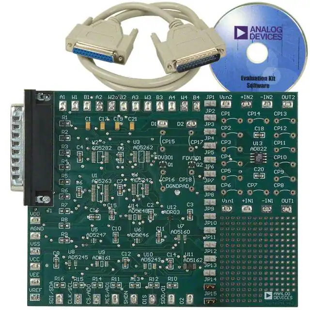


 工商网监
湘ICP备2023018690号
工商网监
湘ICP备2023018690号
