..
,.
ANALOG
W DEVICES
IntegratedCircuit
PrecisionInstrumentation
Amplifier
AD521
[
FEATURES
Programmable Gains from 0.1 to 1000
Differential Inputs
High CMRR: 11OdBmin
Low Drift: 2p.Vfc max (L)
Complete Input Protection, Power ON and Power OFF
Functionally Complete with the Addition of Two Resistors
Internally Compensated
Gain Bandwidth Product: 4OMHz
Output Current Limited: 25mA
Very LowNoise: 05p.V p-p, 0.1Hzto 10Hz, RTI (I G -1000
Chips are Available
Not
Reco
mme
PRODUCT DESCRIPTION
The AD521 is a second generation, low cost, monolithic IC
instrUmentation amplifier developed by Analog Devices.As a
trUe instrUmentation amplifier, the AD521 is a gain block with
differential inputs and an accurately programmable input/
output gain relationship.
The AD521 IC instrUmentation amplifier should not be confused with an operational amplifier, although several manufactUrers(including Analog Devices)offer op amps which can
be used as building blocks in variable gain instrumentation
amplifier circuits. Op amps are general-purpose components
which, when used with precision-matched external resistors,
can perform the instrUmentation amplifier function.
nded
An instrumentation amplifier is a precision differential voltage gain device optimized for operation in a real world environment, and is intended to be used wherever acquisition of a
useful signal is difficult. It is characterized by high input impedance, balanced differential inputs, low bias currents and
high CMR.
As a complete instrUmentation amplifier, the AD521 requires
only two resistors to set its gain to any value between 0.1 and
1000. The ratio matching of these resistors does not affect the
high CMRR (up to 120dB) or the high input impedance (3 X
109il) of the AD521. Furthermore, unlike most operational
amplifier-based instrUmentation amplifiers, the inputs are
protected against overvoltagesup to :1:15volts beyond the
supplies.
The AD521 IC instrumentation amplifier is available in four
different versions of accuracy and operating temperatUre range.
The economical "J" grade, the low drift "K" grade, and the
lower drift, higher linearity "L" grade are specified from 0 to
01::\/
1\
I
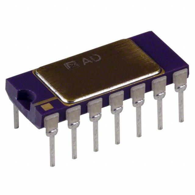
PIN CONFIGURATION
+ INPUT I 1
141 ~AIN
GAI~ 12
131 ~ALE
OFFSET
TRIMI 4
OFFSET
TRIMI 8
9
OUTPUT
81 v+
I 7
a
I COMPo
+70°C.The "S" grade guarantees performance to specification
over the eXtended temperatUre range: -SSoC to +125°C.
PRODUCT HIGHLIGHTS
1. The ADS21 is a trUe instrumentation amplifier in integrated
circuit form, offering the user performance comparable to
many modular instrumentation amplifiers at a fraction of
the cost.
for n
ew D
esig
2. The AD521 has low guaranteed input offset voltage drift
(21lVf C for L grade) and low noise for precision, high gain
applications.
ns
3. The AD521 is functionally complete with the addition of
two resistors. Gain can be preset from 0.1 to more than
1000.
4. The AD521 is fully protected for input levelsup to 15V
beyond the supply voltages and JOV differential at the
inputs.
5. Internally compensated for all gains, the AD521 also offers
the user the provision for limiting bandwidth.
6. Offset nulling can be achieved with an optional trim pot.
7. The AD521 offers superior dynamic performance with a
gain-bandwidth product of 40MHz, full peak response of
100kHz (independent of gain) and a settling time of 5p.s
to 0.1% of a 10V step.
-~ ~--
~_.
~
�AD521* Product Page Quick Links
Last Content Update: 11/01/2016
Comparable Parts
Design Resources
View a parametric search of comparable parts
•
•
•
•
Documentation
Data Sheet
• AD521: Integrated Circuit Precision Instrumentation
Amplifier Data Sheet
Technical Books
• A Designer's Guide to Instrumentation Amplifiers, 3rd
Edition, 2006
AD521 Material Declaration
PCN-PDN Information
Quality And Reliability
Symbols and Footprints
Discussions
View all AD521 EngineerZone Discussions
Sample and Buy
Reference Materials
Visit the product page to see pricing options
Technical Articles
• Auto-Zero Amplifiers
• High-performance Adder Uses Instrumentation Amplifiers
Technical Support
Submit a technical question or find your regional support
number
* This page was dynamically generated by Analog Devices, Inc. and inserted into this data sheet. Note: Dynamic changes to
the content on this page does not constitute a change to the revision number of the product data sheet. This content may be
frequently modified.
�AD521-SPECIFICATIONS
(typical @ Vs = :t15V, RL=
~
AD521JD
GAIN
Ra..e (For Spocified Operation, Note I)
Equation
Error from Equation
Nonlin..rity (NatO 2)
I..G2MHz
300kHz
200kHz
40kHz
75kHz
26kHz
24kHz
6kHz
100kHz
10V/lis
711'
511S
lOlls
35l1s
G. 100
G.lOOO
DifforcntiaJ Overload Recovery (130V Input to within
10mV of Final Value) (NatO 4)
G - 1000
2kO and TA =
mme
SOliS
Common Mode StOp Recovery (30V Input to within
10mV of Final Value) (NatO 5)
G
=1000
VOLTAGE OFFSET (may be nulled)
Input Offset Voltage (Vas,)
vs. Temporature
vs. Supply
Output Offset Voltage (Vaso)
vs. Temporature
vs. Supply (Narc 6)
nded
lOllS
3mV max (2mV typ)
1511VtC max (7I1VtC typ)
311V/%
4OOmV max (200mV typ)
4OOIIVtCmax (l50IlV!':C typ)
0.005VOSO/%
l.5mV max (0.5mV ryp)
511VtC max (l.5I1Vfc typ)
l.Omv max (0.5mV typ)
2IIV/.C max
200mV max (30mV typ)
150llVfc max (50IlV!':C typ)
lOOmV max
7511VtCmax
80nA max
InAtC max
2 %IV
20nA max
4OnA max
250pAtC
125pAtC
INPUT CURRENTS
Input
vs.
vs.
Input
vs.
INPUT
Bias Current (either input)
Temporature
Supply
Offser Current
Temporature
Differential Input Impodance (NatO 7)
Common Mode Input Impedance (NatO 8)
Input Voltage Range for Specified Poriorrnance
(with rospect to ground)
Maximum Voltage without Damage to Unit, Power ON
or OFF Differential Mode (Note 9)
Voltage at either input (Narc 9)
Common Mode Rejection Ratio, DC to 60Hz with IH1
source unbalance
Gol
GolO
GolOO
G . 1000
max
Oporati!ll Voltage Ra..e
Quincent Supply Current
TEMPERATURE RANGE
Spooned Performance
Oporating
Storage
.
500pAfC
max
.
ew . D
esig
10nA max
max
ns
3 x 1O911111.8pF
6 x lO'O11113.0pF
tlOV
30V
Vs tl5V
70dB min (74dB typ)
90dB min (94dB typ)
lOOdB min (l04dB typ)
lOOdB min (lIOdB typ)
NOISE
Voltage RTO (p-p)@O.IHz to 10Hz (Narc 10)
RMS RTO, 10Hz to 10kHz
Input Current, rms, 10Hz to 10kHz
REFERENCE TERMINAL
Bias Current
Input Resistance
Voltage Range
Gain to Output
POWER SUPPLY
fo. r n
74dB min (80dB typ)
94dB min (lOOdB typ)
1O4dB min (l14dB typ)
-
llOdB min (l20dB trP,)
-
-
311A
IOM11
tlOV
I
-
t5V to U8V
SmA max
0 to +70.C
-25.C to +85.C
-65.C to +150.C
-55.Cto+125.C
-55.C to +125.C
--
°Specificatiom
AD521JD.
ooSpec:if'ocatioaa
AD5Z1KD.
Specificatioaaoubjoct10
很抱歉,暂时无法提供与“AD521LD”相匹配的价格&库存,您可以联系我们找货
免费人工找货