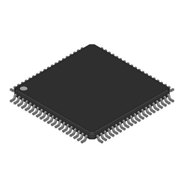
40-Channel, 14-Bit,
Serial Input, Voltage Output DAC
AD5371
FEATURES
40-channel DAC in 80-lead LQFP and 100-ball CSP_BGA
Guaranteed monotonic to 14 bits
Maximum output voltage span of 4 × VREF (20 V)
Nominal output voltage span of −4 V to +8 V
Multiple, independent output voltage spans available
System calibration function allowing user-programmable
offset and gain
Channel grouping and addressing features
Thermal shutdown function
DSP/microcontroller-compatible serial interface
SPI/LVDS serial interface
2.5 V to 5.5 V digital interface
Digital reset (RESET)
Clear function to user-defined SIGGNDx
Simultaneous update of DAC outputs
APPLICATIONS
Level setting in automatic test equipment (ATE)
Variable optical attenuators (VOA)
Optical switches
Industrial control systems
Instrumentation
FUNCTIONAL BLOCK DIAGRAM
VDD
LDAC
14
SPI/LVDS
14
SYNC
SERIAL
INTERFACE
14
14
SDI
SCLK
14
SDO
14
BUSY
M REGISTER
14
14
X2A
REGISTER
X2B
REGISTER
14
MUX 2
TO
MUX2
14
X1A
REGISTER
X1B
REGISTER
14
14
X2B
REGISTER
14
M REGISTER
X2A
REGISTER
14
14
14
14
14
14
14
14
AD5371
14
DAC 7
REGISTER
14
OUTPUT BUFFER
AND
POWER-DOWN
CONTROL
DAC 7
14
A/B SELECT 8
REGISTER
X1A
REGISTER
X1B
REGISTER
M REGISTER
TO
MUX2
14
14
X2A
REGISTER
X2B
REGISTER
14
14
OFS1
REGISTER
14
14
DAC 0
REGISTER
OFFSET
DAC 1
BUFFER
BUFFER
DAC 0
GROUP 1
OUTPUT BUFFER
AND
POWER-DOWN
CONTROL
X1B
REGISTER
M REGISTER
VOUT1
VOUT6
VOUT7
SIGGND0
VREF1
VOUT8
VOUT9
VOUT10
VOUT11
VOUT12
14
C REGISTER
X1A
REGISTER
VOUT0
VOUT2
C REGISTER
MUX 2
STATE
MACHINE
DAC 0
OUTPUT BUFFER
AND
POWER-DOWN
CONTROL
VREF0
VOUT4
VOUT13
14
14
X2A
REGISTER
X2B
REGISTER
14
MUX 2
14
BUFFER
GROUP 0
VOUT5
MUX 1
CLR
14
DAC 0
REGISTER
OFFSET
DAC 0
BUFFER
C REGISTER
MUX 1
8
14
VOUT3
14
RESET
OFS0
REGISTER
14
MUX 2
14
MUX 1
14
A/B SELECT 8
REGISTER
X1A
REGISTER
X1B
REGISTER
MUX 1
8
14
SYNC
AGND DGND
14
CONTROL
REGISTER
SDI
SCLK
VSS
14
14
DAC 7
REGISTER
DAC 7
14
C REGISTER
GROUP 2 TO GROUP 4
ARE SAME AS GROUP 1
SIGGND2
OUTPUT BUFFER
AND
POWER-DOWN
CONTROL
VREF2 SUPPLIES
GROUP 2 TO GROUP 4
SIGGND3
SIGGND4
VOUT14
VOUT15
SIGGND1
VREF2
VOUT16
TO
VOUT39
05814-001
DVCC
Figure 1.
Rev. B
Information furnished by Analog Devices is believed to be accurate and reliable. However, no
responsibility is assumed by Analog Devices for its use, nor for any infringements of patents or other
rights of third parties that may result from its use. Specifications subject to change without notice. No
license is granted by implication or otherwise under any patent or patent rights of Analog Devices.
Trademarks and registered trademarks are the property of their respective owners.
One Technology Way, P.O. Box 9106, Norwood, MA 02062-9106, U.S.A.
Tel: 781.329.4700
www.analog.com
Fax: 781.461.3113 ©2007–2008 Analog Devices, Inc. All rights reserved.
�AD5371
TABLE OF CONTENTS
Features .............................................................................................. 1
Calibration................................................................................... 19
Applications....................................................................................... 1
Additional Calibration............................................................... 19
Functional Block Diagram .............................................................. 1
Reset Function ............................................................................ 20
Revision History ............................................................................... 2
Clear Function ............................................................................ 20
General Description ......................................................................... 3
BUSY and LDAC Functions...................................................... 20
Specifications..................................................................................... 4
Power-Down Mode.................................................................... 20
Performance Specifications......................................................... 4
Thermal Shutdown Function ................................................... 20
AC Characteristics........................................................................ 5
Toggle Mode................................................................................ 21
Timing Characteristics ................................................................ 6
Serial Interface ................................................................................ 22
Absolute Maximum Ratings............................................................ 9
SPI Interface ................................................................................ 22
ESD Caution.................................................................................. 9
LVDS Interface............................................................................ 22
Pin Configurations and Function Descriptions ......................... 10
SPI Write Mode .......................................................................... 22
Typical Performance Characteristics ........................................... 13
SPI Readback Mode ................................................................... 23
Terminology .................................................................................... 15
LVDS Operation ......................................................................... 23
Theory of Operation ...................................................................... 16
Register Update Rates ................................................................ 23
DAC Architecture....................................................................... 16
Channel Addressing and Special Modes ................................. 23
Channel Groups.......................................................................... 16
Special Function Mode.............................................................. 25
A/B Registers and Gain/Offset Adjustment............................ 17
Applications Information .............................................................. 27
Load DAC.................................................................................... 17
Power Supply Decoupling ......................................................... 27
Offset DACs ................................................................................ 17
Power Supply Sequencing ......................................................... 27
Output Amplifier........................................................................ 18
Interfacing Examples ................................................................. 27
Transfer Function ....................................................................... 18
Outline Dimensions ....................................................................... 28
Reference Selection .................................................................... 18
Ordering Guide .......................................................................... 28
REVISION HISTORY
3/08—Rev. A to Rev. B
11/07—Rev. 0 to Rev. A
Added Table 1.................................................................................... 3
Changes to Timing Characteristics Section.................................. 6
Changes to Absolute Maximum Ratings Section......................... 9
Changes to Table 7.......................................................................... 11
Changes to Figure 16, Figure 18, and Figure 19 ......................... 14
Changes to A/B Registers and Gain/Offset Adjustment
Section and Load DAC Section .................................................... 17
Changes to Transfer Function Section......................................... 18
Changes to Calibration Section .................................................... 19
Changes to Reset Function Section and Clear Function
Section.............................................................................................. 20
Changes to Table 9.......................................................................... 20
Changes to Register Update Rates Section.................................. 23
Reformatted Specifications Table 1 .................................................3
Reformatted Specifications Table 2 .................................................6
Change to A/B Registers and Gain/Offset
Adjustment Section ........................................................................ 19
Change to SPI Write Mode Section.............................................. 24
Changes to Ordering Guide .......................................................... 31
8/07—Revision 0: Initial Version
Rev. B | Page 2 of 28
�AD5371
GENERAL DESCRIPTION
The AD5371 1 contains 40 14-bit DACs in a single 80-lead LQFP
or 100-ball CSP_BGA. The device provides buffered voltage
outputs with a span of 4× the reference voltage. The gain and
offset of each DAC can be independently trimmed to remove
errors. For even greater flexibility, the device is divided into five
groups of eight DACs. Three offset DACs allow the output range
of the groups to be adjusted. Group 0 can be adjusted by Offset
DAC 0, Group 1 can be adjusted by Offset DAC 1, and Group 2
to Group 4 can be adjusted by Offset DAC 2.
The AD5371 offers guaranteed operation over a wide supply
range, with VSS from −16.5 V to −4.5 V and VDD from 9 V to
16.5 V. The output amplifier headroom requirement is 1.4 V
operating with a load current of 1 mA.
1
The AD5371 has a high speed serial interface that is compatible
with SPI, QSPI™, MICROWIRE™, and DSP interface standards
and can handle clock speeds of up to 50 MHz. It also has a
100 MHz low voltage differential signaling (LVDS) serial
interface.
The DAC registers are updated on reception of new data. All the
outputs can be updated simultaneously by taking the LDAC
input low. Each channel has a programmable gain and an offset
adjust register to allow removal of gain and offset errors.
Each DAC output is gained and buffered on chip with respect
to an external SIGGNDx input. The DAC outputs can also be
switched to SIGGNDx via the CLR pin.
Protected by U.S. Patent No. 5,969,657; other patents pending.
Table 1. High Channel Count Bipolar DACs
Model
AD5360
AD5361
AD5362
AD5363
AD5370
AD5371
AD5372
AD5373
AD5378
AD5379
Resolution (Bits)
16
14
16
14
16
14
16
14
14
14
Nominal Output Span
4 × VREF (20 V)
4 × VREF (20 V)
4 × VREF (20 V)
4 × VREF (20 V)
4 × VREF (12 V)
4 × VREF (12 V)
4 × VREF (12 V)
4 × VREF (12 V)
±8.75 V
±8.75 V
Output Channels
16
16
8
8
40
40
32
32
32
40
Rev. B | Page 3 of 28
Linearity Error (LSB)
±4
±1
±4
±1
±4
±1
±4
±1
±3
±3
�AD5371
SPECIFICATIONS
PERFORMANCE SPECIFICATIONS
DVCC = 2.5 V to 5.5 V; VDD = 9 V to 16.5 V; VSS = −16.5 V to −8 V; VREF = 3 V; AGND = DGND = SIGGNDx = 0 V; CL = open circuit;
RL = open circuit; gain (M), offset (C), and DAC offset registers at default values; temperature range for the AD5371 is −40°C to +85°C; all
specifications TMIN to TMAX, unless otherwise noted.
Table 2.
Parameter
ACCURACY
Resolution
Integral Nonlinearity (INL)
Differential Nonlinearity (DNL)
Zero-Scale Error
Full-Scale Error
Gain Error
Zero-Scale Error2
Full-Scale Error2
Span Error of Offset DAC
VOUTx Temperature Coefficient
(VOUT0 to VOUT39)
DC Crosstalk2
REFERENCE INPUTS (VREF0, VREF1, VREF2)2
VREFx Input Current
VREFx Range
SIGGND INPUTS (SIGGND0 TO SIGGND4)2
DC Input Impedance
Input Range
SIGGNDx Gain
OUTPUT CHARACTERISTICS2
Output Voltage Range
Nominal Output Voltage Range
Short-Circuit Current
Load Current
Capacitive Load
DC Output Impedance
DIGITAL INPUTS
Input High Voltage
Input Low Voltage
Input Current
CLR High Impedance Leakage Current
Input Capacitance2
DIGITAL OUTPUTS (SDO, BUSY)
Output Low Voltage
Output High Voltage (SDO)
SDO High Impedance Leakage Current
High Impedance Output Capacitance2
Min
Typ1
Max
14
Unit
Test Conditions/Comments1
120
Bits
LSB
LSB
mV
mV
% FSR
LSB
LSB
mV
ppm
FSR/°C
μV
−10
2
+10
5
μA
V
Per input; typically ±30 nA
±2% for specified operation
50
−0.5
0.995
kΩ
V
Typically 55 kΩ
+0.5
1.005
VDD − 1.4
+8
15
+1
2200
0.5
V
V
mA
mA
pF
Ω
ILOAD = 1 mA
0.8
+1
+20
10
V
V
V
μA
μA
pF
DVCC = 2.5 V to 3.6 V
DVCC = 3.6 V to 5.5 V
DVCC = 2.5 V to 5.5 V
Excluding CLR pin
V
V
μA
pF
Sinking 200 μA
Sourcing 200 μA
−1
−1
−10
−10
+1
+1
+10
+10
0.1
1
1
−35
+35
5
VSS + 1.4
−4
−1
1.7
2.0
−1
−20
0.5
DVCC − 0.5
−5
+5
10
Rev. B | Page 4 of 28
Guaranteed monotonic by design
Before calibration
Before calibration
After calibration
After calibration
See the Offset DACs section for details
Includes linearity, offset, and gain drift
Typically 20 μV; measured channel at midscale,
full-scale change on any other channel
VOUTx to DVCC, VDD, or VSS
�AD5371
Parameter
LVDS INTERFACE (REDUCED RANGE LINK)
Digital Inputs2
Input Voltage Range
Input Differential Threshold
External Termination Resistance
Differential Input Voltage
POWER REQUIREMENTS
DVCC
VDD
VSS
Power Supply Sensitivity2
∆Full Scale/∆VDD
∆Full Scale/∆VSS
∆Full Scale/∆DVCC
DICC
Min
875
–0.1
80
100
Typ 1
Max
Unit
100
1575
+0.1
132
mV
V
Ω
mV
5.5
16.5
−4.5
V
V
V
2
dB
dB
dB
mA
2.5
9
−16.5
−75
−75
−90
IDD
18
20
−18
−20
ISS
Power Dissipation Unloaded (P)
Power-Down Mode
DICC
IDD
ISS
Junction Temperature 3
280
5
35
−35
130
mA
mA
mA
mA
mW
μA
μA
μA
°C
Test Conditions/Comments1
DVCC = 5.5 V, VIH = DVCC, VIL = GND; normal
operating conditions
Outputs unloaded, DAC outputs = 0 V
Outputs unloaded, DAC outputs = full scale
Outputs unloaded, DAC outputs = 0 V
Outputs unloaded, DAC outputs = full scale
VSS = −8 V, VDD = 9.5 V, DVCC = 2.5 V
Control register power-down bit set
TJ = TA + PTOTAL × θJA
1
Typical specifications are at 25°C.
Guaranteed by design and characterization; not production tested.
3
θJA represents the package thermal impedance.
2
AC CHARACTERISTICS
DVCC = 2.5 V; VDD = 15 V; VSS = −15 V; VREF = 3 V; AGND = DGND = SIGGNDx = 0 V; CL = 200 pF; RL = 10 kΩ; gain (M), offset (C),
and DAC offset registers at default values; all specifications TMIN to TMAX, unless otherwise noted.
Table 3. AC Characteristics 1
Parameter
DYNAMIC PERFORMANCE
Output Voltage Settling Time
Min
Typ
Max
20
30
Slew Rate
Digital-to-Analog Glitch Energy
Glitch Impulse Peak Amplitude
Channel-to-Channel Isolation
DAC-to-DAC Crosstalk
Digital Crosstalk
Digital Feedthrough
Output Noise Spectral Density @ 10 kHz
1
1
5
10
100
20
0.2
0.02
250
Unit
Test Conditions/Comments
μs
μs
V/μs
nV-s
mV
dB
nV-s
nV-s
nV-s
nV/√Hz
Settling to 1 LSB from a full-scale change
DAC latch contents alternately loaded with all 0s and all 1s
Guaranteed by design and characterization; not production tested.
Rev. B | Page 5 of 28
VREF0, VREF1, VREF2 = 2 V p-p, 1 kHz
Effect of input bus activity on DAC output under test
VREF = 0 V
�AD5371
TIMING CHARACTERISTICS
DVCC = 2.5 V to 5.5 V; VDD = 9 V to 16.5 V; VSS = −16.5 V to −8 V; VREFx = 3 V; AGND = DGND = SIGGNDx = 0 V; CL = 200 pF to GND;
RL = open circuit; gain (M), offset (C), and DAC offset registers at default values; all specifications TMIN to TMAX, unless otherwise noted.
Table 4. SPI Interface
Parameter 1, 2, 3
t1
t2
t3
t4
t5
t6
t7
t8
t9 4
t10
t11
t12
t13
t14
t15
t16
t17
t18
t19
t20
t21
t22 5
t23
Limit at TMIN, TMAX
20
8
8
11
20
10
5
5
42
1/1.5
600
20
10
3
0
3
20/30
140
30
400
270
25
80
Unit
ns min
ns min
ns min
ns min
ns min
ns min
ns min
ns min
ns max
μs typ/μs max
ns max
ns min
ns min
μs max
ns min
μs max
μs typ/μs max
ns max
ns min
μs max
ns min
ns max
ns max
Description
SCLK cycle time
SCLK high time
SCLK low time
SYNC falling edge to SCLK falling edge setup time
Minimum SYNC high time
24th SCLK falling edge to SYNC rising edge
Data setup time
Data hold time
SYNC rising edge to BUSY falling edge
BUSY pulse width low (single-channel update); see Table 9
Single-channel update cycle time
SYNC rising edge to LDAC falling edge
LDAC pulse width low
BUSY rising edge to DAC output response time
BUSY rising edge to LDAC falling edge
LDAC falling edge to DAC output response time
DAC output settling time
CLR/RESET pulse activation time
RESET pulse width low
RESET time indicated by BUSY low
Minimum SYNC high time in readback mode
SCLK rising edge to SDO valid
RESET rising edge to BUSY falling edge
1
Guaranteed by design and characterization; not production tested.
All input signals are specified with tR = tF = 2 ns (10% to 90% of DVCC) and timed from a voltage level of 1.2 V.
3
See Figure 4 and Figure 5.
4
t9 is measured with the load circuit shown in Figure 2.
5
t22 is measured with the load circuit shown in Figure 3.
2
Table 5. LVDS Interface
Parameter 1, 2, 3
t1
t2
t3
t4
t5
t6
t7
1
2
3
Limit at TMIN, TMAX
12
5
5
3
3
3
10
Unit
ns min
ns min
ns min
ns min
ns min
ns min
ns min
Description
SCLK cycle time
SCLK pulse width high and low time
SYNC to SCLK setup time
Data setup time
Data hold time
SCLK to SYNC hold time
SYNC high time
Guaranteed by design and characterization; not production tested.
All input signals are specified with tR = tF = 2 ns (10% to 90% of DVCC) and timed from a voltage level of 1.2 V.
See Figure 6.
Rev. B | Page 6 of 28
�AD5371
Circuit and Timing Diagrams
200µA
IOL
DVCC
VOL
CL
50pF
05814-002
TO
OUTPUT
PIN
VOH (MIN) – VOL (MAX)
2
CL
50pF
200µA
Figure 2. Load Circuit for BUSY Timing Diagram
05814-003
TO OUTPUT
PIN
RL
2.2k Ω
IOH
Figure 3. Load Circuit for SDO Timing Diagram
t1
SCLK
1
24
2
t3
t6
t5
t7
SDI
24
t11
t2
t4
SYNC
1
t8
DB0
DB23
t9
t10
BUSY
t12
t13
LDAC1
t17
t14
VOUTx1
t15
t13
LDAC2
t17
VOUTx2
t16
CLR
t18
VOUTx
t19
RESET
VOUTx
t18
t20
BUSY
05814-004
t23
1 LDAC ACTIVE DURING BUSY.
2 LDAC ACTIVE AFTER BUSY.
Figure 4. SPI Write Timing
Rev. B | Page 7 of 28
�AD5371
t22
SCLK
48
t21
SYNC
DB23
DB0
DB23
INPUT WORD SPECIFIES
REGISTER TO BE READ
DB0
NOP CONDITION
DB0
SDO
DB23
DB15
DB0
05814-005
SDI
SELECTED REGISTER DATA CLOCKED OUT
LSB FROM PREVIOUS WRITE
Figure 5. SPI Read Timing
SYNC
SYNC
t3
t1
t6
SCLK
SDI
MSB
D23
t2
t4
SDI
t5
Figure 6. LVDS Timing
Rev. B | Page 8 of 28
LSB
D0
05814-006
SCLK
�AD5371
ABSOLUTE MAXIMUM RATINGS
TA = 25°C, unless otherwise noted. Transient currents of up to
60 mA do not cause SCR latch-up.
Table 6.
Parameter
VDD to AGND
VSS to AGND
DVCC to DGND
Digital Inputs to DGND
Digital Outputs to DGND
VREF0, VREF1, VREF2 to AGND
VOUT0 through VOUT39 to AGND
SIGGND0 through SIGGND4 to AGND
AGND to DGND
Operating Temperature Range (TA)
Industrial (B Version)
Storage Temperature Range
Operating Junction Temperature
(TJ max)
θJA Thermal Impedance
80-Lead LQFP
100-Ball CSP_BGA
Reflow Soldering
Peak Temperature
Time at Peak Temperature
Rating
−0.3 V to +17 V
−17 V to +0.3 V
−0.3 V to +7 V
−0.3 V to DVCC + 0.3 V
−0.3 V to DVCC + 0.3 V
−0.3 V to +5.5 V
VSS − 0.3 V to VDD + 0.3 V
−1 V to +1 V
−0.3 V to +0.3 V
Stresses above those listed under Absolute Maximum Ratings
may cause permanent damage to the device. This is a stress
rating only; functional operation of the device at these or any
other conditions above those indicated in the operational
section of this specification is not implied. Exposure to absolute
maximum rating conditions for extended periods may affect
device reliability.
ESD CAUTION
−40°C to +85°C
−65°C to +150°C
130°C
38.72°C/W
40°C/W
230°C
10 sec to 40 sec
Rev. B | Page 9 of 28
�AD5371
VOUT5
VOUT6
VOUT7
DGND
DVCC
SYNC
SYNC
SCLK
SCLK
SDI
SDI
SPI/LVDS
TESTO
SDO
DVCC
DGND
AGND
VOUT24
VOUT25
VOUT26
PIN CONFIGURATIONS AND FUNCTION DESCRIPTIONS
80 79 78 77 76 75 74 73 72 71 70 69 68 67 66 65 64 63 62 61
LDAC 1
60
VOUT4
59
NC
RESET 3
58
SIGGND0
BUSY 4
57
VOUT3
TESTI 5
56
VOUT2
VOUT27 6
55
VOUT1
SIGGND3 7
54
VOUT0
VOUT28 8
53
NC
VOUT29 9
52
VREF0
51
NC
50
VREF2
VOUT32 12
49
VOUT23
VOUT33 13
48
VOUT22
VOUT34 14
47
VOUT21
VOUT35 15
46
VOUT20
SIGGND4 16
45
VSS
VOUT36 17
44
VDD
VOUT37 18
43
NC
VDD 19
42
NC
VSS 20
41
SIGGND2
PIN 1
CLR 2
AD5371
VOUT30 10
TOP VIEW
(Not to Scale)
VOUT31 11
Figure 7. 80-Lead LQFP Pin Configuration
Rev. B | Page 10 of 28
05814-007
VOUT19
VOUT18
VOUT17
VOUT16
VOUT15
NC
VOUT14
VOUT13
VOUT12
SIGGND1
VOUT11
VOUT10
VOUT9
VOUT8
VOUT39
VOUT38
NC
NC
NC
VREF1
21 22 23 24 25 26 27 28 29 30 31 32 33 34 35 36 37 38 39 40
NC = NO CONNECT
�AD5371
12
11
10
9
8
7
6
5
4
3
2
1
DGND
DGND
DVCC
SYNC
SCLK
SDI
SPI/
LVDS
TESTO
LDAC
CLR
NC
AGND
A
VOUT6
VOUT7
DVCC
SYNC
SCLK
SDI
NC
SDO
RESET
BUSY
TESTI
AGND
B
VOUT4
VOUT5
AGND
AGND
C
VOUT3
SIGGND0
AGND
VOUT1
VOUT2
VOUT0
AGND
VOUT25 VOUT26
D
AGND
VSS
VOUT24 VOUT27
E
NC
AGND
VSS
NC
SIGGND3
F
VREF0
NC
AGND
VSS
VOUT28
NC
G
VOUT23
VREF2
AGND
VSS
VOUT30 VOUT29
H
VSS
VOUT32 VOUT31
J
VOUT34 VOUT33
K
VDD
VOUT21 VOUT22
AGND
VDD
AGND
VDD
AGND
VDD
AGND
VDD
VOUT20 VOUT19
SIGGND2
VOUT17 VOUT15 VOUT13 SIGGND1 VOUT10
VOUT18 VOUT16 VOUT14 VOUT12 VOUT11
VOUT9
VOUT8
VOUT39
VOUT38 SIGGND4
VREF1
VSS
VOUT37 VOUT36
VOUT35
L
VSS
M
05814-025
VDD
VDD
Figure 8. 100-Ball Grid Array Pin Configuration—Bottom View
Table 7. Pin Function Descriptions
Pin No.
1
Ball No.
A4
Mnemonic
LDAC
2
A3
CLR
3
4
B4
B3
RESET
BUSY
5
73
54 to 57,
60 to 63,
27 to 30,
32 to 34,
36 to 40,
46 to 49,
78 to 80,
6, 8 to 15,
17, 18,
25, 26
B2
A5
F12, E12, E11,
D12, C12, C11,
B12, B11, L5,
M6, L6, M7,
M8, L8, M9, L9,
M10, L10, M11,
K11, K12, J12,
J11, H12, E2,
D2, D1, E1, G2,
H1, H2, J1, J2,
K1, K2, L1, M2,
M3, L4, M5
TESTI
TESTO
VOUT0 to
VOUT39
Description
Load DAC Logic Input (Active Low). See the BUSY and LDAC Functions section for more
information.
Asynchronous Clear Input (Level Sensitive, Active Low). See the Clear Function section for
more information.
Digital Reset Input.
Digital Input/Open-Drain Output. BUSY is open drain when an output. See the BUSY and LDAC
Functions section for more information.
Test Input Pin. Connect this pin to DGND.
Test Output Pin. This pin remains unconnected.
DAC Outputs. Buffered analog outputs for each of the 40 DAC channels. Each analog output
is capable of driving an output load of 10 kΩ to ground. Typical output impedance of these
amplifiers is 0.5 Ω.
Rev. B | Page 11 of 28
�AD5371
Pin No.
58
31
41
7
16
52
21
50
19, 44
64, 76
65, 75
Ball No.
D11
L7
L12
F1
L3
G12
M4
H11
J5 to J9, L11,
M12
E4, F4, G4, H4,
J4, L2, M1
A11, A12
A10, B10
DGND
DVCC
66
A9
SYNC
67
B9
SYNC
68
A8
SCLK
69
B8
SCLK
70
A7
SDI
71
B7
SDI
72
A6
SPI/LVDS
74
B5
SDO
77
A1, B1, C1, C2,
D4 to D9, E9,
F9, G9, H9
A2, B6, F2, F11,
G1, G11
AGND
Description
Reference Ground for DAC 0 to DAC 7. VOUT0 to VOUT7 are referenced to this voltage.
Reference Ground for DAC 8 to DAC 15. VOUT8 to VOUT15 are referenced to this voltage.
Reference Ground for DAC 16 to DAC 23. VOUT16 to VOUT23 are referenced to this voltage.
Reference Ground for DAC 24 to DAC 31. VOUT24 to VOUT31 are referenced to this voltage.
Reference Ground for DAC 32 to DAC 39. VOUT32 to VOUT39 are referenced to this voltage.
Reference Input for DAC 0 to DAC 7. This reference voltage is referred to AGND.
Reference Input for DAC 8 to DAC 15. This reference voltage is referred to AGND.
Reference Input for DAC 16 to DAC 39. This reference voltage is referred to AGND.
Positive Analog Power Supply; 9 V to 16.5 V for specified performance. Decouple these pins
with 0.1 μF ceramic capacitors and 10 μF capacitors.
Negative Analog Power Supply; −16.5 V to −8 V for specified performance. Decouple these
pins with 0.1 μF ceramic capacitors and 10 μF capacitors.
Ground for All Digital Circuitry. Connect both DGND pins to the DGND plane.
Logic Power Supply; 2.5 V to 5.5 V. Decouple these pins with 0.1 μF ceramic capacitors and
10 μF capacitors.
Active Low or Differential SYNC Input (Complement) for SPI or LVDS Interface. This is the
frame synchronization signal for the SPI or LVDS serial interface. See the Timing Characteristics
section for more details.
Differential SYNC Input for LVDS Interface. This is the frame synchronization signal for the
LVDS serial interface. See the Timing Characteristics section for more details.
Serial Clock Input for SPI or LVDS Interface. See the Timing Characteristics section for more
details.
Differential Serial Clock Input (Complement) for LVDS Interface. See the Timing Characteristics
section for more details.
Serial Data Input for SPI or LVDS Interface. See the Timing Characteristics section for more
details.
Differential Serial Data Input (Complement) for LVDS Interface. See the Timing Characteristics
section for more details.
Interface Selection Pin. If the pin is low, the SPI interface is selected. If the pin is high, the
LVDS interface is selected.
Serial Data Output for SPI Interface. CMOS output. SDO can be used for readback. Data is
clocked out on SDO on the rising edge of SCLK and is valid on the falling edge of SCLK.
Ground for All Analog Circuitry. Connect the AGND pin to the AGND plane.
NC
No Connect. Do not connect these pins.
20, 45
22 to 24,
35, 42,
43, 51,
53, 59
Mnemonic
SIGGND0
SIGGND1
SIGGND2
SIGGND3
SIGGND4
VREF0
VREF1
VREF2
VDD
VSS
Rev. B | Page 12 of 28
�AD5371
TYPICAL PERFORMANCE CHARACTERISTICS
0.50
0
TA = 25°C
VSS = –15V
VDD = +15V
VREF = +4.096V
AMPLITUDE (V)
INL (LSB)
0.25
0
–0.01
4096
0
8192
12288
05814-012
–0.50
05814-009
–0.25
–0.02
16383
0
2
4
6
8
10
TIME (µs)
DAC CODE
Figure 9. Typical INL Plot
Figure 12. Analog Crosstalk Due to LDAC
7
0.0050
VDD = +15V
VSS = –15V
TA = 25°C
6
TA = 25°C
VSS = –15V
VDD = +15V
VREF = +4.096V
AMPLITUDE (V)
4
3
2
0
–0.0025
05814-010
1
0
–0.6
–0.3
0
0.3
–0.0050
0.6
05814-013
NUMBER OF UNITS
0.0025
5
0
1
Figure 10. Typical INL Distribution
4
5
1.0
VDD = +15V
VSS = –15V
DVCC = +5V
VREF = +3V
0.5
DNL (LSB)
0.5
0
0
0
20
40
60
80
–1.0
05814-014
–0.5
–0.5
05814-011
INL ERROR (LSB)
3
Figure 13. Digital Crosstalk
1.0
–1.0
2
TIME (µs)
INL (LSB)
0
4096
8192
DAC CODE
TEMPERATURE (°C)
Figure 11. Typical INL Error vs. Temperature
Figure 14. Typical DNL Plot
Rev. B | Page 13 of 28
12288
16383
�600
14
500
12
NUMBER OF UNITS
400
300
200
10
8
6
4
2
05814-015
100
0
VSS = –15V
VDD = +15V
TA = 25°C
0
1
2
3
FREQUENCY (Hz)
4
0
05814-018
OUTPUT NOISE (nV/ Hz)
AD5371
13.00
Figure 15. Output Noise Spectral Density
0.50
13.75
14
14.00
DVCC = 5V
TA = 25°C
12
NUMBER OF UNITS
0.45
DICC (mA)
13.50
IDD (mA)
Figure 18. Typical IDD Distribution
VSS = –12V
VDD = +12V
VREF = +3V
DVCC = +5.5V
0.40
13.25
5
DVCC = +3.6V
0.35
DVCC = +2.5V
10
8
6
4
0.30
–20
0
20
40
60
0
80
TEMPERATURE (°C)
Figure 16. DICC vs. Temperature
IDD
13.0
ISS
12.5
VSS = –12V
VDD = +12V
VREF = +3V
05814-017
IDD/ISS ( |mA| )
13.5
–20
0
20
40
0.30
0.35
0.40
DICC (mA)
0.45
Figure 19. Typical DICC Distribution
14.0
12.0
–40
05814-019
05814-016
0.25
–40
2
60
80
TEMPERATURE (°C)
Figure 17. IDD/ISS vs. Temperature
Rev. B | Page 14 of 28
0.50
�AD5371
TERMINOLOGY
Integral Nonlinearity (INL)
Integral nonlinearity, or endpoint linearity, is a measure of the
maximum deviation from a straight line passing through the
endpoints of the DAC transfer function. It is measured after
adjusting for zero-scale error and full-scale error and is
expressed in least significant bits (LSB).
Differential Nonlinearity (DNL)
Differential nonlinearity is the difference between the measured
change and the ideal 1 LSB change between any two adjacent
codes. A specified differential nonlinearity of 1 LSB maximum
ensures monotonicity.
Zero-Scale Error
Zero-scale error is the error in the DAC output voltage when
all 0s are loaded into the DAC register. Zero-scale error is a
measure of the difference between VOUT (actual) and VOUT
(ideal), expressed in millivolts (mV), when the channel is at its
minimum value. Zero-scale error is mainly due to offsets in the
output amplifier.
Full-Scale Error
Full-scale error is the error in the DAC output voltage when all
1s are loaded into the DAC register. Full-scale error is a measure
of the difference between VOUT (actual) and VOUT (ideal),
expressed in millivolts, when the channel is at its maximum
value. Full-scale error does not include zero-scale error.
Gain Error
Gain error is the difference between full-scale error and
zero-scale error. It is expressed as a percentage of the fullscale range (FSR).
Gain Error = Full-Scale Error − Zero-Scale Error
VOUT Temperature Coefficient
The VOUT temperature coefficient includes output error
contributions from linearity, offset, and gain drift.
DC Output Impedance
DC output impedance is the effective output source resistance.
It is dominated by package lead resistance.
Output Voltage Settling Time
Output voltage settling time is the amount of time it takes for
the output of a DAC to settle to a specified level for a full-scale
input change.
Digital-to-Analog Glitch Energy
Digital-to-analog glitch energy is the amount of energy that is
injected into the analog output at the major code transition. It
is specified as the area of the glitch in nV-s. It is measured by
toggling the DAC register data between 0x1FFF and 0x2000.
Channel-to-Channel Isolation
Channel-to-channel isolation refers to the proportion of input
signal from the reference input of one DAC that appears at the
output of another DAC operating from another reference. It is
expressed in decibels and measured at midscale.
DAC-to-DAC Crosstalk
DAC-to-DAC crosstalk is the glitch impulse that appears at the
output of one converter due to both the digital change and
subsequent analog output change at another converter. It is
specified in nV-s.
Digital Crosstalk
Digital crosstalk is defined as the glitch impulse transferred to
the output of one converter due to a change in the DAC register
code of another converter. It is specified in nV-s.
Digital Feedthrough
When the device is not selected, high frequency logic activity
on the digital inputs of the device can be capacitively coupled
both across and through the device to appear as noise on the
VOUTx pins. It can also be coupled along the supply and
ground lines. This noise is digital feedthrough.
Output Noise Spectral Density
Output noise spectral density is a measure of internally generated random noise. Random noise is characterized as a spectral
density (voltage per √Hz). It is measured by loading all DACs
to midscale and measuring noise at the output. It is measured
in nV/√Hz.
DC Crosstalk
The DAC outputs are buffered by op amps that share common
VDD and VSS power supplies. If the dc load current changes in
one channel (due to an update), this change can result in a
further dc change in one or more channel outputs. This effect is
more significant at high load currents and is reduced as the load
currents are reduced. With high impedance loads, the effect is
virtually immeasurable. Multiple VDD and VSS terminals are
provided to minimize dc crosstalk.
Rev. B | Page 15 of 28
�AD5371
THEORY OF OPERATION
DAC ARCHITECTURE
The AD5371 contains 40 DAC channels and 40 output amplifiers
in a single package. The architecture of a single DAC channel
consists of a 14-bit resistor-string DAC followed by an output
buffer amplifier. The resistor-string section is simply a string of
resistors, of equal value, from VREFx to AGND. This type of
architecture guarantees DAC monotonicity. The 14-bit binary
digital code loaded to the DAC register determines at which
node on the string the voltage is tapped off before being fed into
the output amplifier. The output amplifier multiplies the DAC
output voltage by 4. The nominal output span is 12 V with a 3 V
reference and 20 V with a 5 V reference.
CHANNEL GROUPS
The 40 DAC channels of the AD5371 are arranged into five
groups of eight channels. The eight DACs of Group 0 derive
their reference voltage from VREF0. The eight DACs of Group 1
derive their reference voltage from VREF1. Group 2 to Group 4
derive their reference voltage from VREF2. Each group has its
own signal ground pin.
Table 8. Register Descriptions
Register
Name
X1A
X1B
M
C
X2A
Word
Length
(Bits)
14
14
14
14
14
X2B
14
OFS0
OFS1
OFS2
Control
14
14
14
3
Default
Value
0x1555
0x1555
0x3FFF
0x2000
Not user
accessible
Not user
accessible
Not user
accessible
0x1555
0x1555
0x1555
0x00
A/B Select 0
8
0x00
A/B Select 1
8
0x00
A/B Select 2
8
0x00
A/B Select 3
8
0x00
A/B Select 4
8
0x00
DAC
Description
Input Data Register A. One for each DAC channel.
Input Data Register B. One for each DAC channel.
Gain trim registers. One for each DAC channel.
Offset trim registers. One for each DAC channel.
Output Data Register A. One for each DAC channel. These registers store the final, calibrated DAC
data after gain and offset trimming. They are not readable or directly writable.
Output Data Register B. One for each DAC channel. These registers store the final, calibrated DAC
data after gain and offset trimming. They are not readable or directly writable.
Data registers from which the DACs take their final input data. The DAC registers are updated from
the X2A or X2B register. They are not readable or directly writable.
Offset DAC 0 data register. Sets offset for Group 0.
Offset DAC 1 data register. Sets offset for Group 1.
Offset DAC 2 data register. Sets offset for Group 2 to Group 4.
Bit 2 = A/B.
0 = global selection of X1A input data registers.
1 = global selection of X1B input data registers.
Bit 1 = enable thermal shutdown.
0 = disable thermal shutdown.
1 = enable thermal shutdown.
Bit 0 = software power-down.
0 = software power-up.
1 = software power-down.
Each bit in this register determines if a DAC in Group 0 takes its data from Register X2A or Register X2B.
0 = X2A.
1 = X2B.
Each bit in this register determines if a DAC in Group 1 takes its data from Register X2A or Register X2B.
0 = X2A.
1 = X2B.
Each bit in this register determines if a DAC in Group 2 takes its data from Register X2A or Register X2B.
0 = X2A.
1 = X2B.
Each bit in this register determines if a DAC in Group 3 takes its data from Register X2A or Register X2B.
0 = X2A.
1 = X2B.
Each bit in this register determines if a DAC in Group 4 takes its data from Register X2A or Register X2B.
0 = X2A.
1 = X2B.
Rev. B | Page 16 of 28
�AD5371
A/B REGISTERS AND GAIN/OFFSET ADJUSTMENT
LOAD DAC
Each DAC channel has seven data registers. The actual DAC
data-word can be written to either the X1A or the X1B input
register, depending on the setting of the A/B bit in the control
register. If the A/B bit is 0, data is written to the X1A register.
If the A/B bit is 1, data is written to the X1B register. Note that
this single bit is a global control and affects every DAC channel
in the device. It is not possible to set up the device on a perchannel basis so that some writes are to X1A registers and
some writes are to X1B registers.
All DACs in the AD5371 can be updated simultaneously by
taking LDAC low when each DAC register is updated from
either its X2A or X2B register, depending on the setting of the
A/B select registers. The DAC register is not readable or directly
writable by the user. LDAC can be permanently tied low, and
the DAC output is updated whenever new data appears in the
appropriate DAC register.
MUX
MUX
X1B
REGISTER
X2B
REGISTER
DAC
REGISTER
DAC
C
REGISTER
05814-020
M
REGISTER
Figure 20. Data Registers Associated with Each DAC Channel
Each DAC channel also has a gain (M) register and an offset (C)
register that allow trimming out of the gain and offset errors of
the entire signal chain. Data from the X1A register is operated
on by a digital multiplier and adder controlled by the contents of
the M and C registers. The calibrated DAC data is then stored in
the X2A register. Similarly, data from the X1B register is operated
on by the multiplier and adder and stored in the X2B register.
Although Figure 20 shows a multiplier and adder for each
channel, there is only one multiplier and one adder in the device
shared among all channels. This has implications for the update
speed when several channels are updated simultaneously, as
described in the Register Update Rates section.
Each time data is written to the X1A register, or to the M or C
register with the A/B control bit set to 0, the X2A data is recalculated and the X2A register is automatically updated. Similarly,
X2B is updated each time data is written to X1B, or to M or C
with A/B set to 1. The X2A and X2B registers are not readable
or directly writable by the user.
In addition to the gain and offset trim for each DAC, there are
three 14-bit offset DACs, one for Group 0, one for Group 1, and
one for Group 2 to Group 4. These allow the output range of all
DACs connected to them to be offset within a defined range.
Thus, subject to the limitations of headroom, it is possible to set
the output range of Group 0, Group 1, or Group 2 to Group 4 to
be unipolar positive, unipolar negative, or bipolar, either symmetrical or asymmetrical about 0 V. The DACs in the AD5371 are
factory trimmed with the offset DACs set at their default values.
This results in optimum offset and gain performance for the
default output range and span.
When the output range is adjusted by changing the value of the
offset DAC, an extra offset is introduced due to the gain error of
the offset DAC. The amount of offset is dependent on the magnitude of the reference and how much the offset DAC deviates from
its default value. See the Specifications section for this offset. The
worst-case offset occurs when the offset DAC is at positive or
negative full scale. This value can be added to the offset present
in the main DAC channel to give an indication of the overall
offset for that channel. In most cases, the offset can be removed
by programming the C register of the channel with an appropriate
value. The extra offset caused by the offset DAC needs to be taken
into account only when the offset DAC is changed from its default
value. Figure 21 shows the allowable code range that can be loaded
to the offset DAC, depending on the reference value used. Thus,
for a 5 V reference, the offset DAC should not be programmed
with a value greater than 8192 (0x2000).
Data output from the X2A and X2B registers is routed to the
final DAC register by a multiplexer. Whether each individual
DAC takes its data from the X2A or X2B register is controlled
by an 8-bit A/B select register associated with each group of
eight DACs. If a bit in this register is 0, the DAC takes its data
from the X2A register; if 1, the DAC takes its data from the X2B
register (Bit 0 through Bit 7 control DAC 0 to DAC 7).
Note that because there are 40 bits in five registers, it is possible
to set up, on a per-channel basis, whether each DAC takes its
data from the X2A or X2B register. A global command is also
provided that sets all bits in the A/B select registers to 0 or to 1.
5
RESERVED
4
3
2
1
0
05814-021
X2A
REGISTER
VREF (V)
X1A
REGISTER
OFFSET DACS
0
4096
8192
OFFSET DAC CODE
12288
Figure 21. Offset DAC Code Range
Rev. B | Page 17 of 28
16383
�AD5371
OUTPUT AMPLIFIER
The output amplifiers can swing to 1.4 V below the positive
supply and 1.4 V above the negative supply, which limits how
much the output can be offset for a given reference voltage. For
example, it is not possible to have a unipolar output range of
20 V, because the maximum supply voltage is ±16.5 V.
S1
DAC
CHANNEL
VOUT
R5
60kΩ
R4
60kΩ
R3
20kΩ
DAC_CODE = INPUT_CODE × (M + 1)/214 + C − 213.
where:
M = code in gain register − default code = 214 − 1.
C = code in offset register − default code = 213.
The DAC output voltage is calculated as follows:
R6
10kΩ
S2
VOUT = 4 × VREFx × (DAC_CODE –
OFFSET_CODE)/214 + VSIGGND
CLR
CLR
R1
20kΩ
The input code is the value in the X1A or X1B register that is
applied to the DAC (X1A, X1B default code = 5461).
S3
CLR
SIGGNDx
R2
20kΩ
05814-022
SIGGNDx
OFFSET
DAC
Figure 22. Output Amplifier and Offset DAC
Figure 22 shows details of a DAC output amplifier and its
connections to its corresponding offset DAC. On power-up,
S1 is open, disconnecting the amplifier from the output. S3 is
closed, so the output is pulled to the corresponding SIGGNDx
(R1 and R2 are greater than R6). S2 is also closed to prevent the
output amplifier from being open-loop. If CLR is low at power-up,
the output remains in this condition until CLR is taken high.
The DAC registers can be programmed, and the outputs assume
the programmed values when CLR is taken high. Even if CLR is
high at power-up, the output remains in this condition until
VDD > 6 V and VSS < −4 V and the initialization sequence has
finished. The outputs then go to their power-on default value.
TRANSFER FUNCTION
where:
DAC_CODE should be within the range of 0 to 16,383.
VREF = 3.0 V for a 12 V span and 5.0 V for a 20 V span.
OFFSET_CODE is the code loaded to the offset DAC. On
power-up, the default code loaded to the offset DAC is 5461
(0x1555). With a 3 V reference, this gives a span of −4 V to +8 V.
REFERENCE SELECTION
The AD5371 has three reference input pins. The voltage applied
to the reference pins determines the output voltage span on
VOUT0 to VOUT39. VREF0 determines the voltage span for
VOUT0 to VOUT7 (Group 0), VREF1 determines the voltage
span for VOUT8 to VOUT15 (Group 1), and VREF2 determines the voltage span for VOUT16 to VOUT39 (Group 2 to
Group 4). The reference voltage applied to each VREF pin can
be different, if required, allowing each group to have a different
voltage span. The output voltage range and span can be adjusted
further by programming the offset and gain registers for each
channel and by programming the offset DACs. If the offset and
gain features are not used (that is, the M and C registers are left
at their default values), the required reference levels can be
calculated as follows:
VREF = (VOUTMAX − VOUTMIN)/4
OUTPUT
VOLTAGE
FULL-SCALE
ERROR
+
ZERO-SCALE
ERROR
8V
If the offset and gain features of the AD5371 are used, the
required output range is slightly different. The selected output
range should take into account the system offset and gain errors
that need to be trimmed out. Therefore, the selected output
range should be larger than the actual required range.
ACTUAL
TRANSFER
FUNCTION
IDEAL
TRANSFER
FUNCTION
0
DAC CODE
Calculate the required reference levels as follows:
1.
2.
16383
3.
05814-008
–4V
ZERO-SCALE
ERROR
Figure 23. DAC Transfer Function
4.
5.
The output voltage of a DAC in the AD5371 is dependent on the
value in the input register, the value of the M and C registers,
and the value in the offset DAC.
Rev. B | Page 18 of 28
Identify the nominal output range on VOUT.
Identify the maximum offset span and the maximum gain
required on the full output signal range.
Calculate the new maximum output range on VOUT,
including the expected maximum offset and gain errors.
Choose the new required VOUTMAX and VOUTMIN, keeping
the VOUT limits centered on the nominal values. Note that
VDD and VSS must provide sufficient headroom.
Calculate the value of VREF as follows:
VREF = (VOUTMAX − VOUTMIN)/4
�AD5371
Reference Selection Example
Reducing Full-Scale Error
If
Full-scale error can be reduced as follows:
Nominal output range = 12 V (−4 V to +8 V)
1.
2.
3.
Zero-scale error = ±70 mV
Gain error = ±3%, and
SIGGNDx = AGND = 0 V
4.
Then
Gain error = ±3%
=> Maximum positive gain error = 3%
=> Output range including gain error = 12 + 0.03(12) = 12.36 V
Zero-scale error = ±70 mV
=> Maximum offset error span = 2(70 mV) = 0.14 V
=> Output range including gain error and zero-scale error =
12.36 V + 0.14 V = 12.5 V
AD5371 Calibration Example
This example assumes that a −4 V to +8 V output is required.
The DAC output is set to −4 V but measured at −4.03 V. This
gives a zero-scale error of −30 mV.
1 LSB = 12 V/16,384 = 732.42 μV
VREF calculation
30 mV = 41 LSBs
Actual output range = 12.5 V, that is, −4.25 V to +8.25 V;
VREF = (8.25 V + 4.25 V)/4 = 3.125 V
If the solution yields an inconvenient reference level, the user
can adopt one of the following approaches:
•
•
•
Use a resistor divider to divide down a convenient, higher
reference level to the required level.
Select a convenient reference level above VREF and modify
the gain and offset registers to digitally downsize the reference.
In this way, the user can use almost any convenient reference
level but can reduce the performance by overcompaction of
the transfer function.
Use a combination of these two approaches.
The full-scale error can now be calculated. The output is set to
8 V and a value of 8.02 V is measured. This gives a full-scale
error of +20 mV and a span error of +20 mV − (−30 mV) =
+50 mV.
50 mV = 68 LSBs
The errors can now be removed as follows:
1.
2.
3.
CALIBRATION
The user can perform a system calibration on the AD5371 to
reduce gain and offset errors to below 1 LSB. This reduction is
achieved by calculating new values for the M and C registers and
reprogramming them.
The M and C registers should not be programmed until both
the zero-scale and full-scale errors are calculated.
Reducing Zero-Scale Error
Zero-scale error can be reduced as follows:
1.
2.
3.
Measure the zero-scale error.
Set the output to the highest possible value.
Measure the actual output voltage and compare it to the
required value. Add this error to the zero-scale error. This
is the span error, which includes the full-scale error.
Calculate the number of LSBs equivalent to the span error
and subtract this number from the default value of the M
register. Note that only positive full-scale error can be
reduced.
Set the output to the lowest possible value.
Measure the actual output voltage and compare it to the
required value. This gives the zero-scale error.
Calculate the number of LSBs equivalent to the error and
add this number to the default value of the C register. Note
that only negative zero-scale error can be reduced.
Add 41 LSBs to the default C register value:
8192 + 41 = 8233
Subtract 68 LSBs from the default M register value:
16,383 − 68 = 16,315
Program the M register to 16,315; program the C register
to 8233.
ADDITIONAL CALIBRATION
The techniques described in the previous section are usually
enough to reduce the zero-scale and full-scale errors in most
applications. However, there are limitations whereby the errors
may not be sufficiently reduced. For example, the offset (C)
register can only be used to reduce the offset caused by the
negative zero-scale error. A positive offset cannot be reduced.
Likewise, if the maximum voltage is below the ideal value, that
is, a negative full-scale error, the gain (M) register cannot be
used to increase the gain to compensate for the error.
These limitations can be overcome by increasing the reference
value. With a 3 V reference, a 12 V span is achieved. The ideal
voltage range for the AD5371 is −4 V to +8 V. Using a +3.1 V
reference increases the range to −4.133 V to +8.2667 V. Clearly,
in this case, the offset and gain errors are insignificant, and the
M and C registers can be used to raise the negative voltage to
−4 V and then reduce the maximum voltage to +8 V to give the
most accurate values possible.
Rev. B | Page 19 of 28
�AD5371
RESET FUNCTION
The reset function is initiated by the RESET pin. On the rising
edge of RESET, the AD5371 state machine initiates a reset
sequence to reset the X, M, and C registers to their default values.
This sequence typically takes 300 μs, and the user should not
write to the part during this time. On power-up, it is recommended that the user bring RESET high as soon as possible to
properly initialize the registers.
When the reset sequence is complete (and provided that CLR is
high), the DAC output is at a potential specified by the default
register settings, which is equivalent to SIGGNDx. The DAC
outputs remain at SIGGNDx until the X, M, or C register is
updated and LDAC is taken low. The AD5371 can be returned
to the default state by pulsing RESET low for at least 30 ns. Note
that, because the reset function is triggered by the rising edge,
bringing RESET low has no effect on the operation of the AD5371.
CLEAR FUNCTION
CLR is an active low input that should be high for normal operation. The CLR pin has an internal 500 kΩ pull-down resistor.
When CLR is low, the input to each of the DAC output buffer
stages, VOUT0 to VOUT39, is switched to the externally set
potential on the relevant SIGGNDx pin. While CLR is low, all
LDAC pulses are ignored. When CLR is taken high again, the
DAC outputs return to their previous values. The contents of
the input registers and the DAC registers are not affected by
taking CLR low. To prevent glitches from appearing on the
outputs, bring CLR low before writing to the offset DAC to
adjust the output span.
BUSY AND LDAC FUNCTIONS
The value of an X2 (A or B) register is calculated each time the
user writes new data to the corresponding X1, C, or M register.
During the calculation of X2, the BUSY output goes low. While
BUSY is low, the user can continue writing new data to the X1,
M, or C register (see the Register Update Rates section for more
details), but no DAC output updates can take place.
The BUSY pin is bidirectional and has a 50 kΩ internal pull-up
resistor. When multiple AD5371 devices are used in one system,
the BUSY pins can be tied together. This is useful when it is
required that no DAC in any device be updated until all other
DACs are ready to be updated. When each device has finished
updating the X2 (A or B) register, it releases the BUSY pin. If
another device has not finished updating its X2 register, it holds
BUSY low, thus delaying the effect of LDAC going low.
The DAC outputs are updated by taking the LDAC input low. If
LDAC goes low while BUSY is active, the LDAC event is stored
and the DAC outputs are updated immediately after BUSY goes
high. A user can also hold the LDAC input permanently low.
In this case, the DAC outputs are updated immediately after
BUSY goes high. Whenever the A/B select registers are written
to, BUSY also goes low for approximately 500 ns.
The AD5371 has flexible addressing that allows writing of data
to a single channel, all channels in a group, the same channel in
Group 0 to Group 4, the same channel in Group 1 to Group 4, or
all channels in the device. This means that 1, 4, 5, 8, or 40 DAC
register values may need to be calculated and updated. Because
there is only one multiplier shared among 40 channels, this task
must be done sequentially so that the length of the BUSY pulse
varies according to the number of channels being updated.
Table 9. BUSY Pulse Widths
Action
Loading X1A, X1B, C, or M to 1 channel2
Loading X1A, X1B, C, or M to 5 channels
Loading X1A, X1B, C, or M to 8 channels
Loading X1A, X1B, C, or M to 40 channels
1
2
BUSY Pulse Width1
1.5 μs maximum
3.9 μs maximum
5.7 μs maximum
24.9 μs maximum
BUSY pulse width = ((number of channels + 1) × 600 ns) + 300 ns.
A single channel update is typically 1 μs.
The AD5371 contains an extra feature whereby a DAC register
is not updated unless its X2A or X2B register has been written
to since the last time LDAC was brought low. Normally, when
LDAC is brought low, the DAC registers are filled with the contents
of the X2A or X2B register, depending on the setting of the A/B
select registers. However, the AD5371 updates the DAC register
only if the X2A or X2B data has changed, thereby removing
unnecessary digital crosstalk.
POWER-DOWN MODE
The AD5371 can be powered down by setting Bit 0 in the
control register to 1. This turns off the DACs, thus reducing the
current consumption. The DAC outputs are connected to their
respective SIGGNDx potentials. The power-down mode does
not change the contents of the registers, and the DACs return to
their previous voltage when the power-down bit is cleared to 0.
THERMAL SHUTDOWN FUNCTION
The AD5371 can be programmed to shut down the DACs if
the temperature on the die exceeds 130°C. Setting Bit 1 in the
control register to 1 enables this function (see Table 17). If the
die temperature exceeds 130°C, the AD5371 enters a thermal
shutdown mode that is equivalent to setting the power-down bit
in the control register to 1. To indicate that the AD5371 has
entered thermal shutdown mode, Bit 4 of the control register is
set to 1. The AD5371 remains in thermal shutdown mode, even
if the die temperature falls, until Bit 1 in the control register is
cleared to 0.
Rev. B | Page 20 of 28
�AD5371
TOGGLE MODE
For the data generator example, the user needs only to set the
high and low levels for each channel once by writing to the X1A
and X1B registers. The values of X2A and X2B are calculated and
stored in their respective registers. The calculation delay, therefore,
happens only during the setup phase, that is, when programming
the initial values. To toggle a DAC output between the two levels,
it is only required to write to the relevant A/B select register to
set the MUX2 register bit. Furthermore, because there are eight
MUX2 control bits per register, it is possible to update eight
channels with a single write. Table 10 shows the bits that correspond to each DAC output.
The AD5371 has two X2 registers per channel, X2A and X2B,
that can be used to switch the DAC output between two levels
with ease. This approach greatly reduces the overhead required
by a microprocessor, which would otherwise need to write to
each channel individually. When the user writes to the X1A,
X1B, M, or C register, the calculation engine takes a certain
amount of time to calculate the appropriate X2A or X2B value.
If an application, such as a data generator, requires that the
DAC output switch between two levels only, any method that
reduces the amount of calculation time necessary is advantageous.
Table 10. DACs Selected by A/B Select Registers
A/B Select
Register
0
1
2
3
4
1
Bits1
F7
VOUT7
VOUT15
VOUT23
VOUT31
VOUT39
F6
VOUT6
VOUT14
VOUT22
VOUT30
VOUT38
F5
VOUT5
VOUT13
VOUT21
VOUT29
VOUT37
F4
VOUT4
VOUT12
VOUT20
VOUT28
VOUT36
If the bit is set to 0, Register X2A is selected. If the bit is set to 1, Register X2B is selected.
Rev. B | Page 21 of 28
F3
VOUT3
VOUT11
VOUT19
VOUT27
VOUT35
F2
VOUT2
VOUT10
VOUT18
VOUT26
VOUT34
F1
VOUT1
VOUT9
VOUT17
VOUT25
VOUT33
F0
VOUT0
VOUT8
VOUT16
VOUT24
VOUT32
�AD5371
SERIAL INTERFACE
The AD5371 contains two high speed serial interfaces: an SPIcompatible interface operating at clock frequencies up to 50 MHz
(20 MHz for read operations) and an LVDS interface. To minimize
both the power consumption of the device and the on-chip digital
noise, the interface powers up fully only when the device is being
written to, that is, on the falling edge of SYNC.
SPI WRITE MODE
The AD5371 allows writing of data via the serial interface to
every register directly accessible to the serial interface, that is,
all registers except the X2A, X2B, and DAC registers. The X2A
and X2B registers are updated when the user writes to the X1A,
X1B, M, or C register, and the DAC data registers are updated
by LDAC.
SPI INTERFACE
The serial word (see Table 13) is 24 bits long: 14 of these bits are
data bits; six bits are address bits; two bits are mode bits that
determine what is done with the data; and two bits are reserved.
The serial interface is 2.5 V LVTTL-compatible when operating
from a 2.5 V to 3.6 V DVCC supply. The SPI interface is selected
when the SPI/LVDS pin is held low. It is controlled by four pins,
as described in Table 11.
The serial interface works with both a continuous and a burst
(gated) serial clock. Serial data applied to SDI is clocked into
the AD5371 by clock pulses applied to SCLK. The first falling
edge of SYNC starts the write cycle. At least 24 falling clock edges
must be applied to SCLK to clock in 24 bits of data before SYNC
is taken high again. If SYNC is taken high before the 24th falling
clock edge, the write operation is aborted.
Table 11. Pins That Control the SPI Interface
Pin
SYNC
SDI
SCLK
SDO
Description
Frame synchronization input
Serial data input pin
Clocks data in and out of the device
Serial data output pin for data readback
If a continuous clock is used, SYNC must be taken high before
the 25th falling clock edge. This inhibits the clock within the
AD5371. If more than 24 falling clock edges are applied before
SYNC is taken high again, the input data becomes corrupted. If
an externally gated clock of exactly 24 pulses is used, SYNC can
be taken high any time after the 24th falling clock edge.
When the SPI mode is used, the SYNC, SDI, and SCLK pins
should be connected to DGND either directly or by using pulldown resistors.
LVDS INTERFACE
The LVDS interface uses the same input pins, with the same
designations, as the SPI interface; however, SDO is not used. In
addition, three other pins are provided for the complementary
signals needed for differential operation, as described in Table 12.
The input register addressed is updated on the rising edge of
SYNC. For another serial transfer to take place, SYNC must be
taken low again.
Table 12. Pins That Control the LVDS Interface
Pin
SYNC
SYNC
Description
Differential frame synchronization signal
Differential frame synchronization signal
(complement)
Differential serial data input
Differential serial data input (complement)
Differential serial clock input
Differential serial clock input (complement)
SDI
SDI
SCLK
SCLK
Table 13. Serial Word Bit Assignment
I23
M1
1
I22
M0
I21
A5
I20
A4
I19
A3
I18
A2
I17
A1
I16
A0
I15
D13
I14
D12
I13
D11
I12
D10
I11
D9
I10
D8
I9
D7
I8
D6
I7
D5
Bit I1 and Bit I0 are reserved for future use and should be set to 0 when writing the serial word. These bits read back as 0.
Rev. B | Page 22 of 28
I6
D4
I5
D3
I4
D2
I3
D1
I2
D0
I1 1
0
I01
0
�AD5371
SPI READBACK MODE
REGISTER UPDATE RATES
The AD5371 allows data readback via the serial interface from
every register directly accessible to the serial interface, that is,
all registers except the X2A, X2B, and DAC data registers. To
read back a register, it is first necessary to tell the AD5371
which register is to be read. This is achieved by writing a word
whose first two bits are the Special Function Code 00 to the
device. The remaining bits then determine which register is to
be read back.
The value of the X2A register or the X2B register is calculated
each time the user writes new data to the corresponding X1, C, or
M register. The calculation is performed by a three-stage process.
The first two stages take approximately 600 ns each, and the
third stage takes approximately 300 ns. When the write to the
X1, C, or M register is complete, the calculation process begins.
If the write operation involves the update of a single DAC channel,
the user is free to write to another register, provided that the
write operation does not finish until the first-stage calculation is
complete, that is, 600 ns after the completion of the first write
operation. If a group of channels is being updated by a single
write operation, the first-stage calculation is repeated for each
channel, taking 600 ns per channel. In this case, the user should
not complete the next write operation until this time has elapsed.
If a readback command is written to a special function register,
data from the selected register is clocked out of the SDO pin
during the next SPI operation. The SDO pin is normally threestated but becomes driven as soon as a read command is issued.
The pin remains driven until the register data is clocked out.
See Figure 5 for the read timing diagram. Note that due to the
timing requirements of t22 (25 ns), the maximum speed of the
SPI interface during a read operation should not exceed 20 MHz.
LVDS OPERATION
The LVDS interface operates as follows. Note that, because the
LVDS signals are differential, when a signal goes high, its
complementary signal goes low, and vice versa.
1.
2.
3.
4.
The SYNC signal frames the data. SCLK is initially high.
After SYNC goes high and the SYNC-to-SCLK setup time
has elapsed, SCLK can start to clock in the data.
Data is clocked into the AD5371 on the high-to-low
transition of SCLK and must be stable at this time (observe
setup and hold time specifications).
SYNC can then be taken low after the SCLK-to-SYNC hold
time to latch the data.
The same comments about burst and continuous clocks for the
SPI interface apply to the LVDS interface. However, readback is
not available when using the LVDS interface.
CHANNEL ADDRESSING AND SPECIAL MODES
If the mode bits are not 00, the data-word D13 to D0 is written
to the device. Address Bit A5 to Address Bit A0 determine
which channels are written to, and the mode bits determine to
which register (X1A, X1B, C, or M) the data is written, as shown in
Table 14 and Table 15. Data is to be written to the X1A register
when the A/B bit in the control register is 0, or to the X1B
register when the A/B bit is 1.
Table 14. Mode Bits
M1
1
1
0
0
M0
1
0
1
0
Action
Write to DAC input data (X) register
Write to DAC offset (C) register
Write to DAC gain (M) register
Special function, used in combination
with other bits of the data-word
The AD5371 has very flexible addressing that allows the writing
of data to a single channel, all channels in a group, the same
channel in Group 0 to Group 4, the same channel in Group 1 to
Group 4, or all channels in the device (see Table 15).
Rev. B | Page 23 of 28
�AD5371
Table 15 shows which groups and which channels are addressed for every combination of Address Bit A5 to Address Bit A0.
Table 15. Group and Channel Addressing
Address Bit A2
to Address Bit A0
000
Address Bit A5 to Address Bit A3
011
100
101
Group 2,
Group 3,
Group 4,
Channel 0
Channel 0
Channel 0
000
All groups,
all channels
001
Group 0,
Channel 0
010
Group 1,
Channel 0
000
Group 0,
all channels
Group 0,
Channel 1
Group 1,
Channel 1
Group 2,
Channel 1
Group 3,
Channel 1
Group 4,
Channel 1
010
Group 1,
all channels
Group 0,
Channel 2
Group 1,
Channel 2
Group 2,
Channel 2
Group 3,
Channel 2
Group 4,
Channel 2
011
Group 2,
all channels
Group 0,
Channel 3
Group 1,
Channel 3
Group 2,
Channel 3
Group 3,
Channel 3
Group 4,
Channel 3
100
Group 3,
all channels
Group 0,
Channel 4
Group 1,
Channel 4
Group 2,
Channel 4
Group 3,
Channel 4
Group 4,
Channel 4
101
Group 4,
all channels
Group 0,
Channel 5
Group 1,
Channel 5
Group 2,
Channel 5
Group 3,
Channel 5
Group 4,
Channel 5
110
Reserved
Group 0,
Channel 6
Group 1,
Channel 6
Group 2,
Channel 6
Group 3,
Channel 6
Group 4,
Channel 6
111
Reserved
Group 0,
Channel 7
Group 1,
Channel 7
Group 2,
Channel 7
Group 3,
Channel 7
Group 4,
Channel 7
Rev. B | Page 24 of 28
110
Group 0,
Group 1,
Group 2,
Group 3,
Group 4;
Channel 0
Group 0,
Group 1,
Group 2,
Group 3,
Group 4;
Channel 1
Group 0,
Group 1,
Group 2,
Group 3,
Group 4;
Channel 2
Group 0,
Group 1,
Group 2,
Group 3,
Group 4;
Channel 3
Group 0,
Group 1,
Group 2,
Group 3,
Group 4;
Channel 4
Group 0,
Group 1,
Group 2,
Group 3,
Group 4;
Channel 5
Group 0,
Group 1,
Group 2,
Group 3,
Group 4;
Channel 6
Group 0,
Group 1,
Group 2,
Group 3,
Group 4;
Channel 7
111
Group 1,
Group 2,
Group 3,
Group 4;
Channel 0
Group 1,
Group 2,
Group 3,
Group 4;
Channel 1
Group 1,
Group 2,
Group 3,
Group 4;
Channel 2
Group 1,
Group 2,
Group 3,
Group 4;
Channel 3
Group 1,
Group 2,
Group 3,
Group 4;
Channel 4
Group 1,
Group 2,
Group 3,
Group 4;
Channel 5
Group 1,
Group 2,
Group 3,
Group 4;
Channel 6
Group 1,
Group 2,
Group 3,
Group 4;
Channel 7
�AD5371
SPECIAL FUNCTION MODE
If the mode bits are 00, the special function mode is selected, as shown in Table 16. Bit I21 to Bit I16 of the serial data-word select the special
function, and the remaining bits are data required for execution of the special function, for example, the channel address for data readback.
The codes for the special functions are shown in Table 17. Table 18 shows the addresses for data readback.
Table 16. Special Function Mode
I23
0
I22
0
I21
S5
I20
S4
I19
S3
I18
S2
I17
S1
I16
S0
I15
F15
I14
F14
I13
F13
I12
F12
I11
F11
I10
F10
I9
F9
I8
F8
I7
F7
I6
F6
I5
F5
I4
F4
I3
F3
I2
F2
I1
F1
I0
F0
Table 17. Special Function Codes
Special Function Code
S5 S4 S3 S2 S1 S0
0
0
0
0
0
0
0
0
0
0
0
1
Data (F15 to F0)
0000 0000 0000 0000
XXXX XXXX XXXX X[F2:F0]
0
0
0
0
0
0
0
0
0
0
0
0
0
0
0
0
0
0
0
0
0
0
0
0
0
0
1
1
1
1
0
0
1
1
1
1
0
0
0
0
1
1
0
0
1
1
0
0
1
1
0
1
0
1
0
1
0
1
0
1
XX[F13:F0]
XX[F13:F0]
XX[F13:F0]
See Table 18
XXXX XXXX [F7:F0]
XXXX XXXX [F7:F0]
XXXX XXXX [F7:F0]
XXXX XXXX [F7:F0]
XXXX XXXX [F7:F0]
XXXX XXXX [F7:F0]
0
1
1
1
0
0
Reserved
Action
No operation (NOP).
Write control register.
F4 = overtemperature indicator (read-only bit). This bit should be 0
when writing to the control register.
F3 = reserved. This bit should be 0 when writing to the control register.
F2 = 1: Select Register X1B for input.
F2 = 0: Select Register X1A for input.
F1 = 1: Enable thermal shutdown mode.
F1 = 0: Disable thermal shutdown mode.
F0 = 1: Software power-down.
F0 = 0: Software power-up.
Write data in F13 to F0 to OFS0 register.
Write data in F13 to F0 to OFS1 register.
Write data in F13 to F0 to OFS2 register.
Select register for readback.
Write data in F7 to F0 to A/B Select Register 0.
Write data in F7 to F0 to A/B Select Register 1.
Write data in F7 to F0 to A/B Select Register 2.
Write data in F7 to F0 to A/B Select Register 3.
Write data in F7 to F0 to A/B Select Register 4.
Block write to A/B select registers.
F7 to F0 = 0: Write all 0s (all channels use the X2A register).
F7 to F0 = 1: Write all 1s (all channels use the X2B register).
Rev. B | Page 25 of 28
�AD5371
Table 18. Address Codes for Data Readback 1
F15
0
0
0
0
1
1
1
1
1
1
1
1
1
1
F14
0
0
1
1
0
0
0
0
0
0
0
0
0
F13
0
1
0
1
0
0
0
0
0
0
0
0
0
F12
F11
F10
F9
F8
F7
Bit F12 to Bit F7 select the channel to be read back,
from Channel 0 = 001000 to Channel 39 = 101111
0
0
0
0
0
0
0
0
0
0
0
0
0
0
0
0
0
0
0
0
0
0
0
0
1
1
1
0
0
0
1
1
1
0
0
0
Bit F6 to Bit F0 are don’t cares for the data readback function.
Rev. B | Page 26 of 28
0
1
1
0
1
1
0
0
1
1
0
1
0
0
1
0
1
0
Register Read
X1A register
X1B register
C register
M register
Control register
OFS0 data register
OFS1 data register
OFS2 data register
A/B Select Register 0
A/B Select Register 1
A/B Select Register 2
A/B Select Register 3
A/B Select Register 4
�AD5371
APPLICATIONS INFORMATION
INTERFACING EXAMPLES
The SPI interface of the AD5371 is designed to allow the
part to be easily connected to industry-standard DSPs and
microcontrollers. Figure 24 shows how the AD5371 connects to
the Analog Devices, Inc., Blackfin® DSP. The Blackfin has an
integrated SPI port that can be connected directly to the SPI
pins of the AD5371, as well as programmable input/output pins
that can be used to set or read the state of the digital input or
output pins associated with the interface.
The AD5371 should have ample supply decoupling of 10 μF in
parallel with 0.1 μF on each supply, located as close to the package
as possible, ideally right up against the device. The 10 μF capacitors
are the tantalum bead type. The 0.1 μF capacitor should have low
effective series resistance (ESR) and low effective series inductance
(ESI)—typical of the common ceramic types that provide a low
impedance path to ground at high frequencies—to handle transient
currents due to internal logic switching.
Avoid digital lines running under the device because they can
couple noise onto the device. Allow the analog ground plane,
however, to run under the AD5371 to avoid noise coupling. The
power supply lines of the AD5371 should use as large a trace as
possible to provide low impedance paths and reduce the effects of
glitches on the power supply line. Shield fast switching digital
signals with digital ground to avoid radiating noise to other
parts of the board, and never run them near the reference
inputs. It is essential to minimize noise on all VREF lines.
Avoid crossover of digital and analog signals. Run traces on
opposite sides of the board at right angles to each other. This
reduces the effects of feedthrough through the board. A microstrip
technique is by far the best approach, but it is not always possible
with a double-sided board. In this technique, the component side
of the board is dedicated to ground plane, while signal traces
are placed on the solder side.
AD5371
SPISELx
SYNC
SCK
SCLK
MOSI
SDI
MISO
SDO
PF10
RESET
PF9
LDAC
PF8
CLR
PF7
BUSY
ADSP-BF531
05814-023
In any circuit where accuracy is important, careful consideration
of the power supply and ground return layout helps to ensure
the rated performance. Design the PCB on which the AD5371 is
mounted so that the analog and digital sections are separated
and confined to certain areas of the board. If the AD5371 is in a
system where multiple devices require an AGND-to-DGND
connection, make the connection at one point only. Establish the
star ground point as close as possible to the device. For supplies
with multiple pins (VSS, VDD, DVCC), it is recommended that
these pins be tied together and that each supply be decoupled
only once.
negative supplies are connected. This is required to prevent
currents from flowing in directions other than toward an analog
or digital ground.
Figure 24. Interfacing to a Blackfin DSP
The Analog Devices ADSP-21065L is a floating-point DSP with
two serial ports (SPORTs). Figure 25 shows how one SPORT
can be used to control the AD5371. In this example, the transmit
frame synchronization (TFSx) pin is connected to the receive
frame synchronization (RFSx) pin. Similarly, the transmit and
receive clocks (TCLKx and RCLKx) are also connected. The user
can write to the AD5371 by writing to the transmit register of
the ADSP-21065L. A read operation can be accomplished by
first writing to the AD5371 to tell the part that a read operation
is required. A second write operation with an NOP instruction
causes the data to be read from the AD5371. The DSP receive
interrupt can be used to indicate when the read operation is
complete.
As is the case for all thin packages, care must be taken to avoid
flexing the package and to avoid a point load on the surface of
this package during the assembly process.
POWER SUPPLY SEQUENCING
When the supplies are connected to the AD5371, it is important
that the AGND and DGND pins be connected to the relevant
ground plane before the positive or negative supplies are applied.
In most applications, this is not an issue because the ground pins
for the power supplies are connected to the ground pins of the
AD5371 via ground planes. When the AD5371 is to be used in a
hot-swap card, care should be taken to ensure that the ground
pins are connected to the supply grounds before the positive or
Rev. B | Page 27 of 28
AD5371
ADSP-21065L
TFSx
RFSx
TCLKx
SYNC
RCLKx
SCLK
DTxA
SDI
DRxA
SDO
FLAG0
RESET
FLAG1
LDAC
FLAG2
CLR
FLAG3
BUSY
Figure 25. Interfacing to an ADSP-21065L DSP
05814-024
POWER SUPPLY DECOUPLING
�AD5371
OUTLINE DIMENSIONS
0.75
0.60
0.45
14.20
14.00 SQ
13.80
1.60
MAX
80
61
60
1
PIN 1
12.20
12.00 SQ
11.80
TOP VIEW
(PINS DOWN)
1.45
1.40
1.35
0.15
0.05
0.20
0.09
7°
3.5°
0°
0.08
COPLANARITY
SEATING
PLANE
20
41
21
VIEW A
VIEW A
40
0.50
BSC
LEAD PITCH
0.27
0.22
0.17
051706-A
ROTATED 90° CCW
COMPLIANT TO JEDEC STANDARDS MS-026-BDD
Figure 26. 80-Lead Low Profile Quad Flat Package [LQFP]
ST-80-1
Dimensions shown in millimeters
A1 CORNER
INDEX AREA
10.00
BSC SQ
12 11 10 9
8 7 6 5 4 3 2 1
A
2.50 SQ
BALL A1
PAD CORNER
TOP VIEW
8.80
BSC SQ
B
C
D
E
F
G
H
J
K
L
M
BOTTOM
VIEW
0.80 BSC
1.40
1.35
1.20
DETAIL A
0.65 REF
DETAIL A
1.11
1.01
0.91
0.34 NOM
0.29 MIN
SEATING
PLANE
0.12 MAX
COPLANARITY
*COMPLIANT TO JEDEC STANDARDS MO-205AC
WITH THE EXCEPTION TO BALL DIAMETER.
012006-0
*0.50
0.45
0.40
BALL DIAMETER
Figure 27. 100-Ball Chip Scale Package Ball Grid Array [CSP_BGA]
(BC-100-2)
Dimensions shown in millimeters
ORDERING GUIDE
Model
AD5371BSTZ 1
AD5371BSTZ-REEL1
AD5371BBCZ1
AD5371BBCZ-REEL1
EVAL-AD5371EBZ1
1
Temperature Range
−40°C to +85°C
−40°C to +85°C
−40°C to +85°C
−40°C to +85°C
Package Description
80-Lead Low Profile Quad Flat Package [LQFP]
80-Lead Low Profile Quad Flat Package [LQFP]
100-Ball Chip Scale Package Ball Grid Array (CSP_BGA)
100-Ball Chip Scale Package Ball Grid Array (CSP_BGA)
Evaluation Board
Z = RoHS Compliant Part.
©2007–2008 Analog Devices, Inc. All rights reserved. Trademarks and
registered trademarks are the property of their respective owners.
D05814-0-3/08(B)
Rev. B | Page 28 of 28
Package Option
ST-80-1
ST-80-1
BC-100-2
BC-100-2
�