16-Channel, 12-/16-Bit nanoDAC+ with 2 ppm/°C Voltage
Reference Temperature Coefficient, SPI Interface
AD5674/AD5674R/AD5679/AD5679R
Data Sheet
FEATURES
FUNCTIONAL BLOCK DIAGRAM
VLOGIC
VDD
VREF
AD5679R/AD5679/AD5674R/AD5674
2.5V REF 1
INPUT
REGISTER
DAC
REGISTER
STRING
DAC 0
INPUT
REGISTER
DAC
REGISTER
STRING
DAC 1
INPUT
REGISTER
DAC
REGISTER
STRING
DAC 2
INPUT
REGISTER
DAC
REGISTER
STRING
DAC 3
SDO
INPUT
REGISTER
DAC
REGISTER
STRING
DAC 14
LDAC
INPUT
REGISTER
DAC
REGISTER
STRING
DAC 15
BUFFER
VOUT0
BUFFER
VOUT1
SCLK
INTERFACE LOGIC
SYNC
SDI
BUFFER
VOUT2
BUFFER
VOUT3
BUFFER
VOUT14
BUFFER
VOUT15
RESET
POWER-ON
RESET
GAIN
×1/×2
POWER-DOWN
LOGIC
GAIN
1ONLY APPLICABLE TO AD5679R/AD5674R.
GND
Figure 1.
APPLICATIONS
Optical transceivers
Base station power amplifiers
Process control (programmable logic controller (PLC)
input/output cards)
Industrial automation
Data acquisition systems
GENERAL DESCRIPTION
The AD5674/AD5674R/AD5679/AD5679R are low power,
16-channel, 12-/16-bit, buffered voltage output, digital-toanalog converters (DACs) that include a 2.5 V, 2 ppm/°C internal
reference (enabled by default), and a gain select pin, resulting
in a full-scale output of 2.5 V (gain = 1) or 5 V (gain = 2). The
devices operate from a single, 2.7 V to 5.5 V supply range and
are guaranteed monotonic by design. The AD5674/AD5674R/
AD5679/AD5679R are available in a 28-lead lead frame chip scale
package (LFCSP) and incorporate a power-on reset (POR) circuit
that ensures that the DAC outputs power up to and remains at
zero-scale or midscale until a valid write. The AD5674/AD5674R/
AD5679/AD5679R contain a power-down mode that reduces
the current consumption to 2 μA typical.
Table 1. Octal and 16-Channel nanoDAC+® Devices
No. of
Channels
8
Interface
SPI1
Reference
Internal
External
16-Bit
AD5676R
AD5676
16
I2C
SPI
Internal
Internal
External
AD5675R
AD5679R
AD5679
PRODUCT HIGHLIGHTS
1.
2.
3.
Rev. B
12-Bit
AD5672R
Not
applicable
AD5671R
AD5674R
AD5674
High channel density: 16 channels in 4 mm × 4 mm
LFCSP.
High relative accuracy (integral nonlinearity (INL))
±4 LSB maximum.
Low drift, 2.5 V, on-chip reference.
Document Feedback
Information furnished by Analog Devices is believed to be accurate and reliable. However, no
responsibilityis assumedby Analog Devices for its use, nor for anyinfringements of patents or other
rights of third parties that may result from its use. Specifications subject to change without notice.
No license is granted by implication or otherwise under any patent or patent rights of Analog
Devices.Trademarks and registered trademarks are the property of their respective owners.
One Technology Way, P.O. Box 9106, Norwood, MA 02062-9106, U.S.A.
Tel: 781.329.4700
©2019 Analog Devices, Inc. All rights reserved.
Technical Support
www.analog.com
17326-001
High performance
High relative accuracy (INL): ±4 LSB maximum at 16 bits
(AD5679/AD5679R)
TUE: ±0.14% of FSR maximum
Offset error: ±1.5 mV maximum
Gain error: ±0.06% of FSR maximum
Low drift, 2.5 V voltage reference temperature coefficient:
2 ppm/°C typical
40 mA short-circuit current
Wide operating ranges
−40°C to +125°C temperature range
2.7 V to 5.5 V power supply range
Simplified implementation
User selectable gain of 1 or 2 (GAIN pin)
1.8 V logic compatibility
50 MHz serial peripheral interface (SPI) with readback or
daisy chain
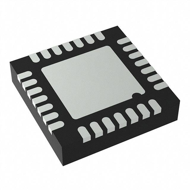
28-lead, 4 mm × 4 mm, RoHS compliant LFCSP
�AD5674/AD5674R/AD5679/AD5679R
Data Sheet
TABLE OF CONTENTS
Features .............................................................................................. 1
Write and Update Commands .................................................. 25
Applications ....................................................................................... 1
Daisy-Chain Operation ............................................................. 25
Functional Block Diagram .............................................................. 1
Readback Operation .................................................................. 25
General Description ......................................................................... 1
Power-Down Operation ............................................................ 26
Product Highlights ........................................................................... 1
Load DAC (Hardware LDAC Pin) ........................................... 27
Revision History ............................................................................... 2
LDAC Mask Register ................................................................. 27
Specifications..................................................................................... 3
Hardware Reset (RESET) .......................................................... 28
AD5674/AD5674R Specifications .............................................. 3
Power-On Reset Internal Circuit.............................................. 28
AD5679/AD5679R Specifications .............................................. 5
Software Reset ............................................................................. 28
AC Characteristics ........................................................................ 7
Internal Reference Setup ........................................................... 28
Timing Characteristics ................................................................ 7
Solder Heat Reflow ..................................................................... 28
Daisy-Chain and Readback Timing Characteristics................ 8
Long-Term Temperature Drift ................................................. 29
Absolute Maximum Ratings .......................................................... 10
Thermal Hysteresis .................................................................... 29
Thermal Resistance .................................................................... 10
Applications Information .............................................................. 30
ESD Caution ................................................................................ 10
Power Supply Recommendations............................................. 30
Pin Configuration and Function Descriptions ........................... 11
Microprocessor Interfacing ....................................................... 30
Typical Performance Characteristics ........................................... 12
Terminology .................................................................................... 21
AD5674/AD5674R/AD5679/AD5679R to ADSP-BF531
Interface ....................................................................................... 30
Theory of Operation ...................................................................... 23
AD5674/AD5674R/AD5679/AD5679R to SPORT Interface30
DAC .............................................................................................. 23
Layout Guidelines....................................................................... 30
Transfer Function ....................................................................... 23
Galvanically Isolated Interface ................................................. 31
DAC Architecture ....................................................................... 23
Outline Dimensions ....................................................................... 32
Serial Interface ............................................................................ 23
Ordering Guide .......................................................................... 32
Standalone Operation ................................................................ 25
REVISION HISTORY
12/2019—Rev. A to Rev. B
Changes to General Description .................................................... 1
Table 2 and Endnote 1...................................................................... 4
Changes to Table 3 ............................................................................ 5
Changes to Table 9 .......................................................................... 11
Changes to Figure 9 ........................................................................ 12
Changes to Figure 13 to Figure 18................................................ 13
Changes to Figure 19 to Figure 24................................................ 14
Changes to Figure 25 to Figure 30................................................ 15
Changes to Figure 31 and Figure 32............................................. 16
Changes to Hardware Reset (RESET) Section and Figure 52 and
Figure 53, Moved Table 19............................................................. 19
Added Figure 60 and Changes to Internal Reference Section .. 24
Instantaneous DAC Updating (LDAC Held Low) and Deferred
DAC Updating (LDAC is Pulsed Low) Sections ........................ 28
Hardware Reset (RESET) Section ................................................ 29
Changes to Ordering Guide .......................................................... 32
11/2019—Rev. 0 to Rev. A
Added AD5674, AD5674R, and AD5679................... Throughout
Changes to Functional Block Diagram, Table 1, General
Description Section, and Product Highlights Section .................1
Changes to Table 2.............................................................................4
Added AD5679/AD5679R Specifications Section and Table 2;
Renumbered Sequentially ................................................................6
Changes to Thermal Resistance Section ..................................... 11
Changes to Figure 7 to Figure 12.................................................. 12
Changes to Figure 13 to Figure 18 ............................................... 13
Changes to Figure 19 to Figure 24 ............................................... 14
Changes to Figure 25 to Figure 30 ............................................... 15
Changes to Figure 31 to Figure 36 ............................................... 16
Changes to Figure 37 to Figure 42 ............................................... 17
Changes to Figure 60...................................................................... 25
Added Long-Term Temperature Drift Section and Figure 64;
Renumbered Sequentially ............................................................. 28
Changes to Figure 67 and Figure 68 ............................................ 30
Changes to Ordering Guide .......................................................... 32
8/2019—Revision 0: Initial Version
Rev. B | Page 2 of 32
�Data Sheet
AD5674/AD5674R/AD5679/AD5679R
SPECIFICATIONS
AD5674/AD5674R SPECIFICATIONS
VDD pin voltage (VDD) = 2.7 V to 5.5 V, 1.62 V ≤ VLOGIC pin voltage (VLOGIC) ≤ 5.5 V, load resistance (RL) = 2 kΩ, load capacitance
(CL) = 200 pF, all specifications are TJ = −40°C to +125°C, typical at TA = 25°C, unless otherwise noted.
Table 2.
Parameter
STATIC PERFORMANCE 1
Resolution
INL
Min
Zero Code Error
Offset Error
Full-Scale Error
Gain Error
Total Unadjusted Error (TUE)
Offset Error Drift
DC Power Supply Rejection Ratio
(PSRR)
DC Crosstalk
OUTPUT CHARACTERISTICS
Output Power-Up Voltage
Load Regulation
Short-Circuit Current 2
Load Impedance at Rails 3
Power-Up Time 4
REFERENCE INPUT
Reference Input Current
±1
±1
±0.1
±0.1
1.6
±2
±1.5
±0.14
±0.07
±0.12
±0.06
±0.18
±0.14
Unit
Test Conditions/Comments
Bits
LSB
LSB
LSB
LSB
mV
mV
mV
% of FSR
% of FSR
% of FSR
% of FSR
% of FSR
% of FSR
µV/°C
mV/V
Gain = 1
Gain = 2
Gain = 1
Gain = 2
Gain = 1 or gain = 2
Gain = 1
Gain = 2
Gain = 1
Gain = 2, VDD = 5.5 V
Gain = 1
Gain = 2
Gain = 1
Gain = 2
Gain = 1
DAC code = midscale, VDD = 5 V ± 10%
±2
µV
±3
±2
µV/mA
µV
0
0
1.25
2.5
2
10
183
V
V
V
V
V
V
nF
nF
µV/mA
177
µV/mA
40
25
3
mA
Ω
µs
0.8
1.6
VDD
VDD/2
mA
mA
V
V
kΩ
kΩ
2.5025
5
V
ppm/°C
2.5
5
1
1
Reference Input Impedance
REFERENCE OUTPUT
Output Voltage 5
Voltage Reference Temperature
Coefficient (TC) 6, 7
±0.12
±0.12
±0.05
±0.05
0.8
−0.75
−0.1
−0.018
−0.013
+0.04
−0.02
±0.03
±0.006
±2
0.25
0
0
Capacitive Load Stability
Reference Input Range
Max
12
Differential Nonlinearity (DNL)
Output Voltage Range
Typ
7
3.5
2.4975
2
Rev. B | Page 3 of 32
Due to single channel, full-scale output change, internal
reference, gain = 1
Due to load current change, external reference, gain = 2
Due to powering down (per channel), internal reference,
gain = 1
Gain = 1, AD5674-1, AD5674R-1
Gain = 2, AD5674-1, AD5674R-1
Gain = 1, AD5674R-2
Gain = 2, AD5674R-2
Gain = 1
Gain = 2
RL = ∞
RL = 1 kΩ
VDD = 5 V ± 10%, DAC code = midscale, −30 mA ≤ output
current (IOUT) ≤ +30 mA
VDD = 3 V ± 10%, DAC code = midscale, −20 mA ≤ IOUT ≤
+20 mA
Exiting power-down mode, VDD = 5 V
Reference voltage (VREF) = VDD = VLOGIC = 5.5 V, gain = 1
VREF = VDD = VLOGIC = 5.5 V, gain = 2
Gain = 1
Gain = 2
Gain = 1
Gain = 2
AD5674R-1; AD5674R-2
See the Terminology section
�AD5674/AD5674R/AD5679/AD5679R
Parameter
Output Impedance
Output Voltage Noise
Output Voltage Noise Density
Min
Load Regulation Sourcing
Load Regulation Sinking
Output Current Load Capability
Line Regulation
Long-Term Stability Drift
Thermal Hysteresis
Typ
0.04
13
240
VDD
Supply Current (IDD)
Normal Mode 8
All Power-Down Modes 9
Max
±1
µA
Per pin
0.3 ×
VLOGIC
V
V
pF
4
0.4
V
V
pF
5.5
1
1.3
0.5
1.3
5.5
5.5
V
µA
µA
µA
µA
V
V
2.53
3.8
2.6
4.2
3.4
5
11
mA
mA
mA
mA
µA
µA
µA
VLOGIC − 0.4
9
2.7
VREF + 1.5
2.3
3.4
2.3
3.4
2
2
2
Test Conditions/Comments
µV/mA
µV/mA
mA
µV/V
ppm
ppm
ppm
0.7 × VLOGIC
1.62
Unit
Ω
µV p-p
nV/√Hz
0.1 Hz to 10 Hz
At ambient temperature (TA), f = 10 kHz, CL = 10 nF, gain =
1 or 2
At ambient temperature
At ambient temperature
VDD ≥ 3 V
At ambient temperature
After 1000 hours at 25°C
First cycle
Additional cycles
29
74
±20
43
77
125
25
LOGIC INPUTS
Input Current
Input Voltage (VIN)
Low (VINL)
High (VINH)
Pin Capacitance
LOGIC OUTPUTS (SDO)
Output Voltage (VOUT)
Low (VOL)
High (VOH)
Floating State Output Capacitance
POWER REQUIREMENTS
VLOGIC
ILOGIC
Data Sheet
Sink current (ISINK) = 200 μA
Source current (ISOURCE) = 200 μA
Power-on, −40°C to +105°C
Power-on, −40°C to +125°C
Power-down, −40°C to +105°C
Power-down, −40°C to +125°C
Gain = 1
Gain = 2
VINH = VDD, VINL = GND, VDD = 2.7 V to 5.5 V
Internal reference off, −40°C to +85°C
Internal reference on, −40°C to +85°C
Internal reference off
Internal reference on
Power-down to 1 kΩ, −40°C to +85°C
Power-down to 1 kΩ, −40°C to +105°C
Power-down to 1 kΩ, −40°C to +125°C
DC specifications tested with the outputs unloaded, unless otherwise noted. Upper dead band = 10 mV and exists only when VREF = VDD with gain = 1, or when VREF/2 =
VDD with gain = 2. Linearity calculated using a reduced code range of 256 to 4080.
2
VDD = 5 V. The device includes current limiting intended to protect the devices during temporary overload conditions. Junction temperature (TJ) can be exceeded
during current limit. Operation above the specified maximum operation junction temperature can impair device reliability.
3
When drawing a load current at either rail, the output voltage headroom with respect to that rail is limited by the 25 Ω typical channel resistance of the output
devices. For example, when sinking 1 mA, the minimum output voltage = 25 Ω × 1 mA = 25 mV.
4
Time to exit power-down to normal mode of operation, SYNC rising edge to 90% of DAC midscale value, with output unloaded.
5
Initial accuracy presolder reflow is ±750 µV. Output voltage includes the effects of preconditioning drift. See the Internal Reference Setup section.
6
Reference is trimmed and tested at two temperatures and is characterized from −40°C to +125°C.
7
Voltage reference temperature coefficient is calculated as per the box method. See the Terminology section for further information.
8
Interface inactive. All DACs active. DAC outputs unloaded.
9
All DACs powered down.
1
Rev. B | Page 4 of 32
�Data Sheet
AD5674/AD5674R/AD5679/AD5679R
AD5679/AD5679R SPECIFICATIONS
VDD = 2.7 V to 5.5 V, 1.62 V ≤ VLOGIC ≤ 5.5 V, RL = 2 kΩ, CL = 200 pF, all specifications are TJ = −40°C to +125°C, typical at TA = 25°C,
unless otherwise noted.
Table 3.
Parameter
STATIC PERFORMANCE 1
Resolution
INL
Min
Zero Code Error
Offset Error
Full-Scale Error
Gain Error
TUE
Offset Error Drift
DC PSRR
DC Crosstalk
OUTPUT CHARACTERISTICS
Output Power-Up Voltage
Load Regulation
Short-Circuit Current 2
Load Impedance at Rails 3
Power-Up Time 4
REFERENCE INPUT
Reference Input Current
Reference Input Impedance
±1.8
±1.7
±0.7
±0.5
0.8
−0.75
−0.1
−0.018
±4
±4
±1
±1
1.6
±2
±1.5
±0.14
−0.013
±0.07
+0.04
±0.12
−0.02
±0.06
±0.03
±0.18
±0.006
±0.14
Unit
Test Conditions/Comments
±2
0.25
±2
Bits
LSB
LSB
LSB
LSB
mV
mV
mV
% of
FSR
% of
FSR
% of
FSR
% of
FSR
% of
FSR
% of
FSR
µV/°C
mV/V
µV
±3
±2
µV/mA
µV
0
0
1.25
2.5
2
10
183
V
V
V
V
V
V
nF
nF
µV/mA
177
µV/mA
40
25
3
mA
Ω
µs
Exiting power-down mode, VDD = 5 V
0.8
1.6
mA
mA
V
V
kΩ
kΩ
VREF = VDD = VLOGIC = 5.5 V, gain = 1
VREF = VDD = VLOGIC = 5.5 V, gain = 2
Gain = 1
Gain = 2
Gain = 1
Gain = 2
0
0
Capacitive Load Stability
Reference Input Range
Max
16
DNL
Output Voltage Range
Typ
2.5
5
1
1
VDD
VDD/2
7
3.5
Rev. B | Page 5 of 32
Gain = 1
Gain = 2
Gain = 1
Gain = 2
Gain = 1 or gain = 2
Gain = 1
Gain = 2
Gain = 1
Gain = 2, VDD = 5.5 V
Gain = 1
Gain = 2
Gain = 1
Gain = 2
Gain = 1
DAC code = midscale, VDD = 5 V ± 10%
Due to single channel, full-scale output change, internal
reference, gain = 1
Due to load current change, external reference, gain = 2
Due to powering down (per channel), internal reference,
gain = 1
Gain = 1, AD5679-1, AD5679R-1
Gain = 2, AD5679-1, AD5679R-1
Gain = 1, AD5679R-2
Gain = 2, AD5679R-2
Gain = 1
Gain = 2
RL = ∞
RL = 1 kΩ
VDD = 5 V ± 10%, DAC code = midscale, −30 mA ≤ IOUT ≤
+30 mA
VDD = 3 V ± 10%, DAC code = midscale, −20 mA ≤ IOUT ≤
+20 mA
�AD5674/AD5674R/AD5679/AD5679R
Parameter
REFERENCE OUTPUT
Output Voltage 5
Voltage Reference TC 6, 7
Output Impedance
Output Voltage Noise
Output Voltage Noise Density
Load Regulation Sourcing
Load Regulation Sinking
Output Current Load Capability
Line Regulation
Long-Term Stability Drift
Thermal Hysteresis
LOGIC INPUTS
Input Current
VIN
VINL
VINH
Pin Capacitance
LOGIC OUTPUTS (SDO)
VOUT
VOL
VOH
Floating State Output Capacitance
POWER REQUIREMENTS
VLOGIC
ILOGIC
VDD
Min
Typ
2.4975
2
0.04
13
240
29
74
±20
43
77
125
25
Data Sheet
Max
Unit
2.5025
5
V
ppm/°C
Ω
µV p-p
nV/√Hz
µV/mA
µV/mA
mA
µV/V
ppm
ppm
ppm
0.1 Hz to 10 Hz
At TA, f = 10 kHz, CL = 10 nF, gain = 1 or 2
At ambient temperature
At ambient temperature
VDD ≥ 3 V
At ambient temperature
After 1000 hours at 25°C
First cycle
Additional cycles
±1
µA
Per pin
0.3 × VLOGIC
V
V
0.7 ×
VLOGIC
4
0.4
9
2.7
VREF + 1.5
V
V
All Power-Down Modes 9
2.3
3.4
2.3
3.4
2
2
2
ISINK = 200 μA
ISOURCE = 200 μA
pF
5.5
1
1.3
0.5
1.3
5.5
5.5
V
µA
µA
µA
µA
V
V
2.53
3.8
2.6
4.2
3.4
5
11
mA
mA
mA
mA
µA
µA
µA
IDD
Normal Mode 8
See the Terminology section
pF
VLOGIC −
0.4
1.62
Test Conditions/Comments
AD5679R-1; AD5679R-2
Power-on, −40°C to +105°C
Power-on, −40°C to +125°C
Power-down, −40°C to +105°C
Power-down, −40°C to +125°C
Gain = 1
Gain = 2
VINH = VDD, VINL = GND, VDD = 2.7 V to 5.5 V
Internal reference off, −40°C to +85°C
Internal reference on, −40°C to +85°C
Internal reference off
Internal reference on
Power-down to 1 kΩ, −40°C to +85°C
Power-down to 1 kΩ, −40°C to +105°C
Power-down to 1 kΩ, −40°C to +125°C
DC specifications tested with the outputs unloaded, unless otherwise noted. Upper dead band = 10 mV and exists only when VREF = VDD with gain = 1, or when VREF/2 =
VDD with gain = 2. Linearity calculated using a reduced code range of 256 to 65,280.
2
VDD = 5 V. The device includes current limiting intended to protect the devices during temporary overload conditions. TJ can be exceeded during current limit.
Operation above the specified maximum operation junction temperature can impair device reliability.
3
When drawing a load current at either rail, the output voltage headroom with respect to that rail is limited by the 25 Ω typical channel resistance of the output
devices. For example, when sinking 1 mA, the minimum output voltage = 25 Ω × 1 mA = 25 mV.
4
Time to exit power-down to normal mode of operation, SYNC rising edge to 90% of DAC midscale value, with output unloaded.
5
Initial accuracy presolder reflow is ±750 µV. Output voltage includes the effects of preconditioning drift. See the Internal Reference Setup section.
6
Reference is trimmed and tested at two temperatures and is characterized from −40°C to +125°C.
7
Voltage reference temperature coefficient is calculated as per the box method. See the Terminology section for further information.
8
Interface inactive. All DACs active. DAC outputs unloaded.
9
All DACs powered down.
1
Rev. B | Page 6 of 32
�Data Sheet
AD5674/AD5674R/AD5679/AD5679R
AC CHARACTERISTICS
VDD = 2.7 V to 5.5 V, 1.62 V ≤ VLOGIC ≤ 5.5 V, RL = 2 kΩ to GND, CL = 200 pF to GND, all specifications are TJ = −40°C to +125°C, typical
at TA = 25°C, unless otherwise noted.
Table 4.
Parameter
OUTPUT VOLTAGE SETTLING TIME 1
SLEW RATE
DIGITAL-TO-ANALOG GLITCH IMPULSE1
DIGITAL FEEDTHROUGH1
CROSSTALK1
Digital
Analog
1
2
Min
Typ
6
0.8
1.4
0.13
Max
8
Unit
µs
V/µs
nV-sec
nV-sec
Test Conditions/Comments
¼ to ¾ scale settling to ±2 LSB
1 LSB change around major carry (internal reference, gain = 1)
DAC-to-DAC
TOTAL HARMONIC DISTORTION 2
0.1
−0.25
−1.3
−2.0
−80
nV-sec
nV-sec
nV-sec
nV-sec
dB
OUTPUT NOISE SPECTRAL DENSITY1
OUTPUT NOISE1
SIGNAL-TO-NOISE RATIO (SNR)
300
6
90
nV/√Hz
µV p-p
dB
SPURIOUS-FREE DYNAMIC RANGE
(SFDR)
SIGNAL-TO-NOISE-AND-DISTORTION
RATIO (SINAD)
83
dB
80
dB
Internal reference, gain = 2
Internal reference, gain = 2
At TA, bandwidth = 20 kHz, VDD = 5 V, output frequency (fOUT) = 1 kHz,
internal reference, gain = 2
DAC code = midscale, 10 kHz, gain = 2
0.1 Hz to 10 Hz, gain = 1
At TA = 25°C, bandwidth = 20 kHz, VDD = 5 V, fOUT = 1 kHz, internal
reference
At TA = 25°C, bandwidth = 20 kHz, VDD = 5 V, fOUT = 1 kHz, internal
reference
At TA = 25°C, bandwidth = 20 kHz, VDD = 5 V, fOUT = 1 kHz, internal
reference, gain = 2
See the Terminology section. Measured using internal reference and gain = 1, unless otherwise noted.
Digitally generated sine wave (fOUT) at 1 kHz.
TIMING CHARACTERISTICS
All input signals are specified with rise time (tR) = fall time (tF) = 1 ns/V (10% to 90% of VDD) and timed from a voltage level of (VINL +
VINH)/2. See Figure 2. VDD = 2.7 V to 5.5 V, 1.62 V ≤ VLOGIC ≤ 5.5 V. VREF = 2.5 V. All specifications are TJ = −40°C to +125°C, unless
otherwise noted.
Table 5.
Parameter
SCLK Cycle Time
SCLK High Time
SCLK Low Time
SYNC to SCLK Falling Edge Setup Time
Data Setup Time
Data Hold Time
SCLK Falling Edge to SYNC Rising Edge
Minimum SYNC High Time
SYNC Rising Edge to SYNC Rising Edge (DAC Register Updates)
SYNC Falling Edge to SCLK Fall Ignore
LDAC Pulse Width Low
SYNC Rising Edge to LDAC Rising Edge
SYNC Rising Edge to LDAC Falling Edge
LDAC Falling Edge to SYNC Rising Edge
Minimum Pulse Width Low
Pulse Activation Time
Symbol
t1
t2
t3
t4
t5
t6
t7
t8
t9
t10
t11
t12
t13
t14
t15
t16
Rev. B | Page 7 of 32
1.62 V ≤ VLOGIC < 2.7 V
Min
Max
20
8
10
15
2
2
4
15
870
4
12
27
25
840
8
115
2.7 V ≤ VLOGIC ≤ 5.5 V
Min
Max
20
8
12
11
3
2
4
12
830
4
12
27
25
840
10
115
Unit
ns
ns
ns
ns
ns
ns
ns
ns
ns
ns
ns
ns
ns
ns
ns
ns
�AD5674/AD5674R/AD5679/AD5679R
t10
Data Sheet
t1
SCLK
t8
t3
t2
t7
t14
t4
SYNC
t9
t6
t5
SDI
DB23
DB0
t11
t13
LDAC1
t12
LDAC2
VOUT
t15
t16
17326-002
RESET
1ASYNCHRONOUS LDAC UPDATE MODE.
2SYNCHRONOUS LDAC UPDATE MODE.
Figure 2. Serial Write Operation
DAISY-CHAIN AND READBACK TIMING CHARACTERISTICS
All input signals are specified with tR = tF = 1 ns/V (10% to 90% of VDD) and timed from a voltage level of (VINL + VINH)/2. See Figure 4 and
Figure 5. VDD = 2.7 V to 5.5 V, 1.62 V ≤ VLOGIC ≤ 5.5 V. VREF = 2.5 V. All specifications are TJ = −40°C to +125°C, unless otherwise noted.
VDD = 2.7 V to 5.5 V.
Table 6.
Parameter
SCLK Cycle Time
SCLK High Time
SCLK Low Time
SYNC to SCLK Falling Edge
Data Setup Time
Data Hold Time
SCLK Falling Edge to SYNC Rising Edge
Minimum SYNC High Time
SDO Data Valid from SCLK Rising Edge
SYNC Rising Edge to SCLK Falling Edge
SYNC Rising Edge to SDO Disable
Symbol
t1
t2
t3
t4
t5
t6
t7
t8
t9
t10
t11
1.62 V ≤ VLOGIC < 2.7 V
Min
Max
130
33
12
80
2
2
35
55
130
15
218
Rev. B | Page 8 of 32
2.7 V ≤ VLOGIC ≤ 5.5 V
Min
Max
110
23
7
80
2
2
10
32
75
8
210
Unit
ns
ns
ns
ns
ns
ns
ns
ns
ns
ns
ns
�Data Sheet
AD5674/AD5674R/AD5679/AD5679R
Circuit and Timing Diagrams
200µA
IOL
VOH (MIN)
SDO
200µA
17326-003
CL
20pF
IOH
Figure 3. Load Circuit for Digital Output (SDO) Timing Specifications
t1
SCLK
24
48
t7
t2
t8
t3
t4
t10
SYNC
t6
DB23
SDI
DB0
DB23
INPUT WORD FOR DAC N
DB0
t9
INPUT WORD FOR DAC N + 1
DB23
SDO
UNDEFINED
DB0
17326-004
t5
INPUT WORD FOR DAC N
Figure 4. Daisy Chain Timing Diagram
t1
SCLK
24
1
t8
t4
t3
24
1
t7
t2
t8
t10
SYNC
t6
t5
DB23
DB0
DB23
INPUT WORD SPECIFIES
REGISTER TO BE READ
DB0
NO OPERATION CONDITION
t9
DB23
SDO
t11
DB0
HIGH-Z
SELECTED REGISTER DATA
CLOCKED OUT
Figure 5. Readback Timing Diagram
Rev. B | Page 9 of 32
17326-005
SDI
�AD5674/AD5674R/AD5679/AD5679R
Data Sheet
ABSOLUTE MAXIMUM RATINGS
TA = 25°C, unless otherwise noted.
THERMAL RESISTANCE
Table 7.
Thermal performance is directly linked to printed circuit board
(PCB) design and operating environment. Careful attention to
PCB thermal design is required.
Parameter
VDD to GND
VLOGIC to GND
VOUTX to GND
VREF to GND
Digital Input Voltage to GND
Operating Junction Temperature
Range
Storage Temperature Range
Absolute Maximum Junction
Temperature
Reflow Soldering Peak Temperature,
Pb-Free (J-STD-020)
Rating
−0.3 V to +7 V
−0.3 V to +7 V
−0.3 V to VDD + 0.3 V
−0.3 V to VDD + 0.3 V
−0.3 V to VLOGIC + 0.3
V
−40°C to +125°C
θJA is the natural convection junction to ambient thermal resistance
measured in a one cubic foot, sealed enclosure. θJB is the junction
to board thermal resistance. θJC is the junction to case thermal
resistance. ΨJT is the junction to top thermal characterization
parameter. ΨJB is the junction to board thermal characterization
parameter.
Table 8. Thermal Resistance
−65°C to +150°C
150°C
Package Type1
CP-28-8
260°C
θJA
55.09
θJB
24.49
θJC
19.14
ΨJT
2.62
ΨJB
23.92
Unit
°C/W
Thermal impedance simulated values are based on a JEDEC 2S2P thermal test
board with nine thermal vias. See JEDEC JESD51.
1
Stresses at or above those listed under Absolute Maximum
Ratings may cause permanent damage to the product. This is a
stress rating only; functional operation of the product at these
or any other conditions above those indicated in the operational
section of this specification is not implied. Operation beyond
the maximum operating conditions for extended periods may
affect product reliability.
ESD CAUTION
Rev. B | Page 10 of 32
�Data Sheet
AD5674/AD5674R/AD5679/AD5679R
PIN CONFIGURATION AND FUNCTION DESCRIPTIONS
23 VOUT10
22 VOUT11
26 VOUT3
25 VOUT8
24 VOUT9
28 VOUT1
27 VOUT2
AD5679R/AD5679/AD5674R/AD5674
21 VREF
VOUT0 1
VDD 2
20 RESET
19 SDO
SYNC 3
TOP VIEW
(Not to Scale)
18 VLOGIC
17 LDAC
SDI 5
VOUT12 14
VOUT14 12
VOUT13 13
VOUT6
VOUT5
VOUT4 10
15 GND
VOUT15 11
16 GND
8
9
GAIN 6
VOUT7 7
NOTES
1. EXPOSED PAD. THE EXPOSED PAD MUST BE
TIED TO GND.
17326-006
SCLK 4
Figure 6. Pin Configuration
Table 9. Pin Function Descriptions
Pin No.
1
2
Mnemonic
VOUT0
VDD
3
SYNC
4
SCLK
5
SDI
6
GAIN
7
8
9
10
11
12
13
14
15, 16
17
VOUT7
VOUT6
VOUT5
VOUT4
VOUT15
VOUT14
VOUT13
VOUT12
GND
LDAC
18
19
VLOGIC
SDO
20
RESET
21
VREF
22
23
24
25
26
27
28
VOUT11
VOUT10
VOUT9
VOUT8
VOUT3
VOUT2
VOUT1
EPAD
Description
Analog Output Voltage from DAC 0. The output amplifier has rail-to-rail operation.
Power Supply Input. These devices operate from 2.7 V to 5.5 V. Decouple the VDD supply with a 10 µF capacitor in parallel with a 0.1
µF capacitor to GND.
Active Low Control Input. This is the frame synchronization signal for the input data. When SYNC goes low, data transfers in on
the falling edges of the next 24 clocks.
Serial Clock Input. Data is clocked into the input shift register on the falling edge of the serial clock input. Data transfers at rates
of up to 50 MHz.
Serial Data Input. The AD5674/AD5674R/AD5679/AD5679R has a 24-bit input shift register. Data is clocked into the register on
the falling edge of the serial clock input.
Span Set Pin. When this pin is tied to GND, all sixteen DAC outputs have a span from 0 V to VREF. If this pin is tied to VLOGIC, all
sixteen DACs output a span of 0 V to 2 × VREF.
Analog Output Voltage from DAC 7. The output amplifier has rail-to-rail operation.
Analog Output Voltage from DAC 6. The output amplifier has rail-to-rail operation.
Analog Output Voltage from DAC 5. The output amplifier has rail-to-rail operation.
Analog Output Voltage from DAC 4. The output amplifier has rail-to-rail operation.
Analog Output Voltage from DAC 15. The output amplifier has rail-to-rail operation.
Analog Output Voltage from DAC 14. The output amplifier has rail-to-rail operation.
Analog Output Voltage from DAC 13. The output amplifier has rail-to-rail operation.
Analog Output Voltage from DAC 12. The output amplifier has rail-to-rail operation.
Ground Reference Point for All Circuitry on the Device.
Load DAC. LDAC operates in two modes: asynchronously and synchronously. Pulsing this pin low updates any or all DAC
registers if the input registers have new data, which simultaneously updates all DAC outputs. This pin can also be tied
permanently low.
Digital Power Supply. The voltage on this pin is specified in Table 2 and Table 3 in the Power Requirements section.
Serial Data Output. This pin can be used to daisy-chain a number of devices together, or it can be used for readback. The serial
data transfers on the rising edge of SCLK and is valid on the falling edge.
Asynchronous Reset Input. The RESET input is falling edge sensitive. When RESET is low, all LDAC pulses are ignored. When RESET is
activated, the input register and the DAC register are updated with zero-scale or midscale, depending on the model in use.
Reference Output Voltage. When using the internal reference, this is the reference output pin. This pin is the reference output
by default.
Analog Output Voltage from DAC 11. The output amplifier has rail-to-rail operation.
Analog Output Voltage from DAC 10. The output amplifier has rail-to-rail operation.
Analog Output Voltage from DAC 9. The output amplifier has rail-to-rail operation.
Analog Output Voltage from DAC 8. The output amplifier has rail-to-rail operation.
Analog Output Voltage from DAC 3. The output amplifier has rail-to-rail operation.
Analog Output Voltage from DAC 2. The output amplifier has rail-to-rail operation.
Analog Output Voltage from DAC 1. The output amplifier has rail-to-rail operation.
Exposed Pad. The exposed pad must be tied to GND.
Rev. B | Page 11 of 32
�AD5674/AD5674R/AD5679/AD5679R
Data Sheet
TYPICAL PERFORMANCE CHARACTERISTICS
0.10
2.0
VDD = 5V
TA = 25°C
INTERNAL REFERENCE = 2.5V
1.5
VDD = 5V
TA = 25°C
INTERNAL REFERENCE = 2.5V
0.08
0.06
DNL ERROR (LSB)
INL ERROR (LSB)
1.0
0.5
0
–0.5
0.04
0.02
0
–0.02
–0.04
–1.0
–0.06
–1.5
10000
20000
30000
40000
50000
60000
70000
CODE
–0.10
17326-007
0
0
1500
2000
2500
3000
4500
4000
Figure 10. AD5674/AD5674R DNL Error vs. Code
0.20
0.04
TOTAL UNADJUSTED ERROR (% OF FSR)
0.10
0.05
0
–0.05
–0.10
–0.20
0
500
1000
1500
2000
2500
3000
4500
4000
CODE
0.03
0.02
0.01
0
–0.01
–0.02
17326-301
–0.15
VDD = 5V
TA = 25°C
INTERNAL REFERENCE = 2.5V
0
10000
20000
30000
40000
50000
60000
17326-009
VDD = 5V
TA = 25°C
INTERNAL REFERENCE = 2.5V
0.15
70000
CODE
Figure 11. AD5679/AD5679R Total Unadjusted Error vs. Code
Figure 8. AD5674/AD5674R INL Error vs. Code
0.04
1.0
0.8
TOTAL UNADJUSTED ERROR (% OF FSR)
VDD = 5V
TA = 25°C
INTERNAL REFERENCE = 2.5V
0.6
0.4
0.2
0
–0.2
–0.4
–0.6
–1.0
0
10000
20000
30000
40000
50000
60000
CODE
70000
17326-008
–0.8
VDD = 5V
TA = 25°C
INTERNAL REFERENCE = 2.5V
0.03
0.02
0.01
0
–0.01
–0.02
0
500
1000
1500
2000
2500
3000
4500
4000
CODE
Figure 12. AD5674/AD5674R Total Unadjusted Error vs. Code
Figure 9. AD5679/AD5679R DNL Error vs. Code
Rev. B | Page 12 of 32
17326-303
INL ERROR (LSB)
1000
CODE
Figure 7. AD5679/AD5679R INL Error vs. Code
DNL ERROR (LSB)
500
17326-302
–0.08
–2.0
�Data Sheet
AD5674/AD5674R/AD5679/AD5679R
2
4
VDD = 5V
INTERNAL REFERENCE = 2.5V
VDD = 5V
INTERNAL REFERENCE = 2.5V
1
DNL ERROR (LSB)
2
1
0
20
40
60
80
100
120
TEMPERATURE (°C)
–2
–40
17326-010
–20
0
20
40
60
80
100
120
TEMPERATURE (°C)
Figure 16. AD5674/AD5674R DNL Error vs. Temperature
Figure 13. AD5679/AD5679R INL Error vs. Temperature
2
0.030
1
0
–2
–40
–20
0
20
40
60
80
100
120
TEMPERATURE (°C)
0.025
0.020
0.015
0.010
0.005
0
–40
17326-304
–1
VDD = 5V
INTERNAL REFERENCE = 2.5V
–20
0
20
40
60
80
100
120
TEMPERATURE (°C)
17326-012
TOTAL UNADJUSTED ERROR (% OF FSR)
VDD = 5V
INTERNAL REFERENCE = 2.5V
INL ERROR (LSB)
–20
17326-305
–1
0
–40
Figure 17. AD5679/AD5679R Total Unadjusted Error vs. Temperature
Figure 14. AD5674/AD5674R INL Error vs. Temperature
0.030
2.0
TOTAL UNADJUSTED ERROR (% OF FSR)
VDD = 5V
INTERNAL REFERENCE = 2.5V
1.5
1.0
0.5
0
–40
–20
0
20
40
60
80
100
120
TEMPERATURE (°C)
Figure 15. AD5679/AD5679R DNL Error vs. Temperature
VDD = 5V
INTERNAL REFERENCE = 2.5V
0.025
0.020
0.015
0.010
0.005
0
–40
17326-011
DNL ERROR (LSB)
0
–20
0
20
40
60
TEMPERATURE (°C)
80
100
120
17326-306
INL ERROR (LSB)
3
Figure 18. AD5674/AD5674R Total Unadjusted Error vs. Temperature
Rev. B | Page 13 of 32
�AD5674/AD5674R/AD5679/AD5679R
Data Sheet
0.10
2.0
TA = 25°C
INTERNAL REFERENCE = 2.5V
TA = 25°C
INTERNAL REFERENCE = 2.5V
0.08
DNL ERROR (LSB)
INL ERROR (LSB)
1.5
1.0
0.06
0.04
0.5
3.0
3.3
3.6
3.9
4.2
4.5
4.8
5.1
5.4
SUPPLY VOLTAGE (V)
0
2.7
17326-016
0
2.7
3.6
3.9
4.2
4.5
4.8
5.1
5.4
Figure 22. AD5674/AD5674R DNL Error vs. Supply Voltage
0.150
0.040
0.125
0.100
0.075
0.050
0
2.7
3.0
3.3
3.6
3.9
4.2
4.5
4.8
5.1
5.4
SUPPLY VOLTAGE (V)
Figure 20. AD5674/AD5674R INL Error vs. Supply Voltage
TA = 25°C
INTERNAL REFERENCE = 2.5V
0.030
0.025
0.020
0.015
0.010
0.005
0
2.7
17326-307
0.025
0.035
3.0
3.3
3.6
3.9
4.2
4.5
4.8
5.1
5.4
SUPPLY VOLTAGE (V)
17326-115
TOTAL UNADJUSTED ERROR (% OF FSR)
TA = 25°C
INTERNAL REFERENCE = 2.5V
Figure 23. AD5679/AD5679R Total Unadjusted Error vs. Supply Voltage
0.020
1.00
TOTAL UNADJUSTED ERROR (% OF FSR)
TA = 25°C
INTERNAL REFERENCE = 2.5V
0.75
0.50
0
2.7
3.0
3.3
3.6
3.9
4.2
4.5
4.8
5.1
5.4
SUPPLY VOLTAGE (V)
Figure 21. AD5679/AD5679R DNL Error vs. Supply Voltage
TA = 25°C
INTERNAL REFERENCE = 2.5V
0.010
0.005
0
–0.005
–0.010
–0.015
–0.020
2.7
17326-017
0.25
0.015
3.0
3.3
3.6
3.9
4.2
4.5
SUPPLY VOLTAGE (V)
4.8
5.1
5.4
17326-309
INL ERROR (LSB)
3.3
SUPPLY VOLTAGE (V)
Figure 19. AD5679/AD5679R INL Error vs. Supply Voltage
DNL ERROR (LSB)
3.0
17326-308
0.02
Figure 24. AD5674/AD5674R Total Unadjusted Error vs. Supply Voltage
Rev. B | Page 14 of 32
�Data Sheet
AD5674/AD5674R/AD5679/AD5679R
0.05
0.020
VDD = 5V
INTERNAL REFERENCE = 2.5V
GAIN ERROR AND
FULL-SCALE ERROR (% OF FSR)
0.005
FULL-SCALE ERROR
0
–0.005
GAIN ERROR
–0.015
0.03
0.02
0.01
0
GAIN ERROR
–0.01
FULL-SCALE ERROR
–0.02
–0.03
–0.04
–20
0
20
40
60
80
100
120
TEMPERATURE (°C)
–0.05
2.7
17326-019
–0.020
–40
3.2
3.7
4.2
4.7
17326-311
GAIN ERROR AND
FULL-SCALE ERROR (% OF FSR)
0.010
–0.010
TA = 25°C
INTERNAL REFERENCE = 2.5V
0.04
0.015
5.2
TEMPERATURE (°C)
Figure 28. AD5674/AD5674R Gain Error and Full-Scale Error vs. Supply
Voltage
Figure 25. AD5679/AD5679R Gain Error and Full-Scale Error vs.
Temperature
0.03
FULL-SCALE ERROR
0.01
GAIN ERROR
–0.01
–0.03
–20
0
20
40
60
80
100
120
TEMPERATURE (°C)
ZERO CODE ERROR
0.9
0.6
0.3
OFFSET ERROR
0
–0.3
–20
0
20
40
60
80
100
120
Figure 29. AD5679/AD5679R Zero Code Error and Offset Error vs.
Temperature
ZERO CODE ERROR AND OFFSET ERROR (mV)
0.03
TA = 25°C
INTERNAL REFERENCE = 2.5V
0.02
0.01
GAIN ERROR
0
–0.01
FULL-SCALE ERROR
–0.02
1.8
VDD = 5V
INTERNAL REFERENCE = 2.5V
1.5
1.2
ZERO-CODE ERROR
0.9
0.6
0.3
OFFSET ERROR
0
–0.3
–0.6
–40
–20
0
20
40
60
80
100
120
TEMPERATURE (°C)
3.0
3.3
3.6
3.9
4.2
4.5
SUPPLY VOLTAGE (V)
4.8
5.1
5.4
17326-020
GAIN ERROR AND
FULL-SCALE ERROR (% OF FSR)
1.2
TEMPERATURE (°C)
Figure 26. AD5674/AD5674R Gain Error and Full-Scale Error vs.
Temperature
–0.03
2.7
VDD = 5V
INTERNAL REFERENCE = 2.5V
–0.6
–40
17326-310
–0.05
–40
1.5
Figure 27. AD5679/AD5679R Gain Error and Full-Scale Error vs. Supply
Voltage
Rev. B | Page 15 of 32
Figure 30. AD5674/AD5674R Zero Code Error and Offset Error vs.
Temperature
17326-312
GAIN ERROR AND
FULL-SCALE ERROR (% OF FSR)
VDD = 5V
INTERNAL REFERENCE = 2.5V
17326-021
ZERO CODE ERROR AND OFFSET ERROR (mV)
1.8
0.05
�Data Sheet
1.4
1.5
1.0
SOURCING – VDD = 5V; G = 1
SOURCING – VDD = 2.7V; G = 1
SOURCING – VDD = 5.5V; G = 2
SOURCING – VDD = 3.3V; G = 1
SINKING – VDD = 5V; G = 1
SINKING – VDD = 2.7V; G = 1
SINKING – VDD = 5.5V; G = 2
SINKING – VDD = 3.3V; G = 1
1.0
ZERO CODE ERROR
0.4
0.5
∆VOUT (V)
ZERO CODE ERROR AND OFFSET ERROR (mV)
AD5674/AD5674R/AD5679/AD5679R
OFFSET ERROR
0
0.2
–0.2
–0.5
–0.6
–1.0
–1.0
TA = 25°C
INTERNAL REFERENCE = 2.5V
3.7
4.2
4.7
5.2
SUPPLY VOLTAGE (V)
–1.4
0
0.015
0.020
0.025
0.030
Figure 34. Headroom and Footroom (ΔVOUT) vs. Load Current
1.5
4.0
0xFFFF
0xC000
0x8000
0x4000
0x0000
3.5
1.0
0.010
LOAD CURRENT (A)
Figure 31. AD5679/AD5679R Zero Code Error and Offset Error vs. Supply
Voltage
ZERO CODE ERROR AND OFFSET ERROR (mV)
0.005
17326-314
3.2
17326-022
–1.5
2.7
3.0
ZERO-CODE ERROR
2.5
VOUT (V)
0.5
0
OFFSET ERROR
REQUIRED VDD HEADROOM
TO MAINTAIN VOUTx = 2.5V
2.0
1.5
1.0
–0.5
0.5
–0.5
4.7
–1.0
–0.06
17326-313
TA = 25°C
INTERNAL REFERENCE = 2.5V
–1.5
2.7
3.2
3.7
4.2
5.2
SUPPLY VOLTAGE (V)
50
–0.04
–0.02
0
0.02
0.04
0.06
OUTPUT CURRENT (A)
Figure 35. Source and Sink Capability at VDD = 3 V
Figure 32. AD5674/AD5674R Zero Code Error and Offset Error vs. Supply
Voltages
60
VDD = 3V
TA = 25°C
GAIN = 1
INTERNAL REFERENCE = 2.5V
17326-026
0
–1.0
6
VDD = 5.5V
GAIN = 2
TA = 25°C
INTERNAL REFERENCE = 2.5V
REQUIRED VDD HEADROOM
TO MAINTAIN VOUTx = 5V
5
4
3
VOUT (V)
HITS
40
30
2
1
20
–1
3330 3350 3370 3390 3410 3430 3450 3470 3490 3510 3530 3550
IDD FULLSCALE (µA)
–2
–0.06
17326-209
0
0xFFFF
0xC000
0x8000
0x4000
0x0000
–0.04
VDD = 5V
TA = 25°C
GAIN = 2
INTERNAL REFERENCE = 2.5V
–0.02
0
0.02
0.04
OUTPUT CURRENT (A)
Figure 36. Source and Sink Capability at VDD = 5 V
Figure 33. Supply Current (IDD) Histogram with Internal Reference
Rev. B | Page 16 of 32
0.06
17326-025
0
10
�Data Sheet
7
AD5674/AD5674R/AD5679/AD5679R
6
3.3
0xFFFF
0xC000
0x8000
0x4000
0x0000
VDD = 5.5V
GAIN = 2
TA = 25°C
INTERNAL REFERENCE = 2.5V
GAIN = 1
TA = 25°C
INTERNAL REFERENCE = 2.5V
3.1
5
2.9
4
2.7
3
2.5
2
2.3
1
2.1
0
1.9
–0.04
–0.02
0
0.02
0.04
0.06
OUTPUT CURRENT (A)
EXTERNAL REFERENCE, FULL SCALE
1.7
2.7
17326-224
–1
–0.06
INTERNAL REFERENCE, ZERO SCALE
3.2
3.7
4.2
4.7
17326-208
IDD (mA)
VOUT (V)
INTERNAL REFERENCE, FULL SCALE
5.2
SUPPLY VOLTAGE (V)
Figure 37. Source and Sink Capability at VDD = 5.5 V
Figure 40. IDD vs. Supply Voltage
3.3
3.6
DEVICE 1
DEVICE 2
DEVICE 3
VDD = 5.5V
GAIN = 1
TA = 25°C
INTERNAL REFERENCE = 2.5V
3.1
3.4
2.9
INTERNAL REFERENCE, FULL SCALE
3.2
IDD (mA)
IDD (mA)
2.7
3
2.5
INTERNAL REFERENCE, ZERO SCALE
2.3
2.8
EXTERNAL REFERENCE, FULL SCALE
2.1
2.6
0
10000
20000
30000
40000
50000
60000
70000
CODE
1.7
1.8
17326-206
2.4
3.1
2.8
3.3
3.8
4.3
4.8
5.3
LOGIC INPUT VOLTAGE (V)
Figure 38. IDD vs. Code
3.3
2.3
17326-211
1.9
Figure 41. IDD vs. Logic Input Voltage
2.0
VDD = 5.5V
GAIN = 1
INTERNAL REFERENCE = 2.5V
1.8
1.6
2.9
INTERNAL REFERENCE, FULL SCALE
1.4
INTERNAL REFERENCE, ZERO SCALE
1.0
0.8
2.3
CH 0
CH 1
CH 2
CH 3
CH 4
CH 5
CH 6
CH 7
0.6
EXTERNAL REFERENCE, FULL SCALE
2.1
1.2
0.4
1.9
1.7
–40
0.2
10
60
TEMPERATURE (°C)
110
0
–2
–1
0
1
2
TIME (µs)
Figure 39. IDD vs. Temperature
Figure 42. Settling Time
Rev. B | Page 17 of 32
3
CH 8
CH 9
CH 10
CH 11
CH 12
CH 13
CH 14
CH 15
4
5
17326-205
VOUT (V)
2.5
17326-210
IDD (mA)
2.7
�AD5674/AD5674R/AD5679/AD5679R
0.006
0.004
0.004
0.003
0.002
2
0.002
1
0.001
–0.002
0
0
–0.004
–1
0
0.002
0.004
0.006
0
–0.001
0.010
0.008
ATTACK CHANNEL
CH 11
CH 6
CH 1
CH 12
CH 7
CH 2
CH
13
CH
8
CH 3
CH 14
CH 9
CH 4
CH 15
CH 10
CH 5
–0.006
22.5
VDD = 5V
GAIN = 1
TA = 25°C
INTERNAL REFERENCE
CODE = 0000 TO FFFF
22.7
22.9
23.1
23.3
23.5
15.0
3.0
10.0
24.3
24.5
ATTACK CHANNEL
CH 11
CH 5
CH 0
CH 12
CH 6
CH 1
CH 13
CH 8
CH 2
CH 14
CH 9
CH 3
CH 15
CH 10
CH 4
0.006
AMPLITUDE (V)
2.0
SYNC
5.0
SYNC (V)
7.5
MIDSCALE, GAIN = 1
0.001
2.5
0.5
–0.004
VDD = 5V
GAIN = 1
TA = 25°C
INTERNAL REFERENCE
CODE = 0000 TO FFFF
0
0
–5
0
–2.5
10
5
TIME (µs)
17326-033
VOUT (V)
12.5
–0.5
24.1
0.011
MIDSCALE, GAIN = 2
2.5
1.0
23.9
Figure 46. Analog Crosstalk
Figure 43. POR to 0 V Output
1.5
23.7
TIME (µs)
TIME (Seconds)
–0.009
21.5
21.7
Figure 44. Exiting Power-Down to Midscale
21.9
22.1
22.3 22.5 22.7
TIME (µs)
22.9
23.1
23.3
23.5
Figure 47. DAC-to-DAC Crosstalk
0.008
WITH LOAD CH0
WITH LOAD CH8
0.006
0.004
VDD = 5V
GAIN = 1
TA = 25°C
INTERNAL REFERENCE
CODE = 7FFF TO 8000
ENERGY = 0.636nV
1
0.002
0
–0.002
2
–0.006
22.5
22.7
22.9
23.1
23.3 23.5 23.7
TIME (µs)
23.9
24.1
24.3
24.5
Figure 45. Digital-to-Analog Glitch Impulse
CH1 50.0mV
M1.00s
A CH1
Figure 48. 0.1 Hz to 10 Hz Output Noise
Rev. B | Page 18 of 32
401mV
17326-134
–0.004
17326-203
AMPLITUDE (V)
17326-201
3
0.005
17326-202
VDD (V)
4
0.008
AMPLITUDE (V)
VDD (V)
VOUT0 (V)
VOUT1 (V)
VOUT2 (V)
VOUT3 (V)
VOUT4 (V)
VOUT5 (V)
VOUT6 (V)
VOUT7 (V)
5
0.006
VOUT (V)
6
Data Sheet
�AD5674/AD5674R/AD5679/AD5679R
1200
1000
VOUT AT MS AND RESET (V)
VDD = 5V
TA = 25°C
GAIN = 1
INTERNAL REFERENCE = 2.5V
NSD (nV/√Hz)
800
FULL SCALE
MIDSCALE
ZERO SCALE
600
400
6
0.30
5
0.25
4
0.20
VOUT AT ZS (V)
Data Sheet
0.15
3
RESET
2
0.10
MIDSCALE, GAIN = 1
0.05
1
ZERO SCALE, GAIN = 1
0
0
200
1k
10k
FREQUENCY (Hz)
100k
1M
–0.10
–2
–10
10
Figure 49. Noise Spectral Density (NSD)
–10
1400
INTERNAL REFERENCE NSD (nV/√Hz)
1600
–50
–70
–90
–110
–130
5
10
15
20
FREQUENCY (kHz)
1000
800
600
400
200
10k
100k
1M
2.5020
0nF
0.1nF
1nF
4.7nF
10nF
DEVICE1
DEVICE2
DEVICE3
DEVICE4
DEVICE5
2.5015
2.5010
2.5005
VREF (V)
1.5
1.0
2.5000
2.4995
2.4990
VDD = 5V
GAIN = 1
TA = 25°C
VREF = 2.5V
0.5
0.14
0.15
TIME (ms)
2.4985
0.16
17326-039
VOUT (V)
1k
Figure 53. Internal Reference ND vs. Frequency
2.5
0
0.13
100
FREQUENCY (Hz)
Figure 50. Total Harmonic Distortion (THD) at 1 kHz
2.0
VDD = 5V
TA = 25°C
0
10
17326-204
–150
1200
2.4980
–40
–20
0
20
40
60
80
TEMPERATURE (°C)
Figure 54. VREF vs. Temperature
Figure 51. Settling Time at Various Capacitive Loads
Rev. B | Page 19 of 32
100
120
17326-142
dB LEVEL (dBV)
–30
0
50
Figure 52. Hardware Reset
10
–170
30
TIME (µs)
17326-140
100
17326-043
0
10
17326-042
–0.05
–1
�AD5674/AD5674R/AD5679/AD5679R
Data Sheet
2.5035
TA = 25°C
2.50045
2.50040
2.5020
2.50035
2.5015
DEVICE3
2.50025
2.5005
2.50020
2.5000
2.50015
–0.025
–0.015
–0.005
0.005
0.015
LOAD CURRENT (A)
0.025
0.035
Figure 55. VREF vs. Load Current
DEVICE2
2.50030
2.5010
2.4995
–0.035
DEVICE1
2.50010
2.5
3.0
3.5
4.0
4.5
VDD (V)
Figure 56. VREF vs. VDD
Rev. B | Page 20 of 32
5.0
5.5
17326-144
VREF (V)
2.5025
17326-143
VREF (V)
2.5030
2.50050
VDD = 5V
TA = 25°C
�Data Sheet
AD5674/AD5674R/AD5679/AD5679R
TERMINOLOGY
Relative Accuracy or Integral Nonlinearity (INL)
For the DAC, relative accuracy or integral nonlinearity is a
measurement of the maximum deviation, in LSBs, from a straight
line passing through the endpoints of the DAC transfer function.
Differential Nonlinearity (DNL)
Differential nonlinearity is the difference between the measured
change and the ideal 1 LSB change between any two adjacent
codes. A specified differential nonlinearity of ±1 LSB maximum
ensures monotonicity. These DACs are guaranteed monotonic
by design.
Zero Code Error
Zero code error is a measurement of the output error when zero
code (0x0000) is loaded to the DAC register. The ideal output is
0 V. The zero code error is always positive because the output of
the DAC cannot go below 0 V due to a combination of the offset
errors in the DAC and the output amplifier. Zero code error is
expressed in mV.
Full-Scale Error
Full-scale error is a measurement of the output error when fullscale code (0xFFFF) is loaded to the DAC register. The ideal
output is VDD − 1 LSB. Full-scale error is expressed in percent of
full-scale range (% of FSR).
Gain Error
Gain error is a measure of the span error of the DAC. It is the
deviation in slope of the DAC transfer characteristic from the
ideal expressed as % of FSR.
Offset Error Drift
Offset error drift is a measurement of the change in offset error
with a change in temperature. Offset error drift is expressed in
µV/°C.
Offset Error
Offset error is a measure of the difference between VOUT (actual)
and VOUT (ideal) expressed in mV in the linear region of the
transfer function. Offset error is measured with Code 256 loaded
in the DAC register. Offset error can be negative or positive.
DC Power Supply Rejection Ratio (PSRR)
The dc PSRR indicates how the output of the DAC is affected by
changes in the supply voltage. PSRR is the ratio of the change in
VOUT to a change in VDD for full-scale output of the DAC. PSRR
is measured in mV/V. VREF is held at 2 V, and VDD is varied by
±10%.
Output Voltage Settling Time
The output voltage settling time is the amount of time it takes for
the output of a DAC to settle to a specified level for a ¼ to ¾ fullscale input change and is measured from the rising edge of SYNC.
Digital-to-Analog Glitch Impulse
Digital-to-analog glitch impulse is the impulse injected into the
analog output when the input code in the DAC register changes
state. Digital-to-analog glitch impulse is normally specified as the
area of the glitch in nV-sec, and is measured when the digital
input code is changed by 1 LSB at the major carry transition
(0x7FFF to 0x8000).
Digital Feedthrough
Digital feedthrough is a measure of the impulse injected into the
analog output of the DAC from the digital inputs of the DAC,
but is measured when the DAC output is not updated. Digital
feedthrough is specified in nV-sec and measured with a fullscale code change on the data bus, that is, from all 0s to all 1s
and vice versa.
Reference Feedthrough
Reference feedthrough is the ratio of the amplitude of the signal
at the DAC output to the reference input when the DAC output
is not being updated. Reference feedthrough is expressed in dB.
Noise Spectral Density
Noise spectral density is a measurement of the internally generated
random noise. Random noise is characterized as a spectral density
(nV/√Hz). Noise spectral density is measured by loading the DAC
to midscale and measuring noise at the output. Noise spectral
density is measured in nV/√Hz.
DC Crosstalk
DC crosstalk is the dc change in the output level of one DAC in
response to a change in the output of another DAC. DC crosstalk
is measured with a full-scale output change on one DAC (or soft
power-down and power-up) when monitoring another DAC
kept at midscale. DC crosstalk is expressed in μV.
DC crosstalk due to load current change is a measure of the impact
that a change in load current on one DAC has on another DAC
kept at midscale. DC crosstalk due to load current change is
expressed in μV/mA.
Digital Crosstalk
Digital crosstalk is the glitch impulse transferred to the output
of one DAC at midscale in response to a full-scale code change
(all 0s to all 1s and vice versa) in the input register of another
DAC. Digital crosstalk is measured in standalone mode and is
expressed in nV-sec.
Analog Crosstalk
Analog crosstalk is the glitch impulse transferred to the output
of one DAC due to a change in the output of another DAC.
Analog crosstalk is measured by first loading one of the input
registers with a full-scale code change (all 0s to all 1s and vice
versa). Then, execute a software LDAC and monitor the output
of the DAC whose digital code was not changed. The area of the
glitch is expressed in nV-sec.
Rev. B | Page 21 of 32
�AD5674/AD5674R/AD5679/AD5679R
Data Sheet
Voltage Reference TC
DAC-to-DAC Crosstalk
Voltage reference TC is a measure of the change in the reference
DAC-to-DAC crosstalk is the glitch impulse transferred to the
output voltage with a change in temperature. The voltage
output of one DAC due to a digital code change and subsequent
reference TC is calculated using the box method, which defines
analog output change of another DAC. DAC-to-DAC crosstalk
the TC as the maximum change in the reference output over a
is measured by loading the attack channel with a full-scale code
given temperature range, expressed in ppm/°C, shown in the
change (all 0s to all 1s and vice versa), using the write to and
following equation:
update commands when monitoring the output of the victim
channel that is at midscale. The energy of the glitch is expressed
VREF ( MAX ) − VREF ( MIN )
in nV-sec.
=
TC
× 106
Multiplying Bandwidth
The multiplying bandwidth is a measure of the finite bandwidth
of the amplifiers within the DAC. A sine wave on the reference
(with full-scale code loaded to the DAC) appears on the output.
The multiplying bandwidth is the frequency at which the output
amplitude falls to 3 dB below the input.
Total Harmonic Distortion (THD)
THD is the difference between an ideal sine wave and its
attenuated version using the DAC. The sine wave is used as the
reference for the DAC, and the THD is a measurement of the
harmonics present on the DAC output. THD is measured in dB.
VREF ( NOM ) × Temperature Range
where:
VREF (MAX) is the maximum reference output measured over the
total temperature range.
VREF (MIN) is the minimum reference output measured over the
total temperature range.
VREF (NOM) is the nominal reference output voltage, 2.5 V.
Temperature Range is the specified temperature range of −40°C
to +125°C.
Rev. B | Page 22 of 32
�Data Sheet
AD5674/AD5674R/AD5679/AD5679R
THEORY OF OPERATION
DAC
The AD5674/AD5674R/AD5679/AD5679R are 16-channel,
12-/16-bit, serial input, voltage output DAC with an internal
reference. The device operates from supply voltages of 2.7 V to
5.5 V. Data is written to the AD5674/AD5674R/AD5679/
AD5679R in a 24-bit word format via a 3-wire serial interface.
The AD5674/AD5674R/AD5679/AD5679R incorporate a POR
circuit to ensure that the DAC output powers up to a known
output state. The device also has a software power-down mode
that reduces the typical current consumption to 2 µA.
TRANSFER FUNCTION
The internal reference is on by default.
The gain of the output amplifier can be set to ×1 or ×2 using the
span set pin (GAIN). When the GAIN pin is tied to GND, all
16 DAC outputs have a span from 0 V to VREF. When the GAIN
pin is tied to VLOGIC, all 16 DACs output a span of 0 V to
2 × VREF.
DAC ARCHITECTURE
REF (+)
VOUTx
GAIN
(GAIN = 1 OR 2)
17326-057
GND
Figure 57. Single DAC Channel Architecture Block Diagram
Output Amplifiers
The output buffer amplifier generates rail-to-rail voltages on its
output. The actual range depends on the value of VREF, the gain
setting, the offset error, and the gain error.
Input Shift Register
VREF
The input shift register of the
AD5674/AD5674R/AD5679/AD5679R is 24 bits wide. Data is
loaded MSB first (DB23), and the first four bits are the command
bits, C3 to C0 (see Table 10, followed by the 4-bit DAC address
bits, A3 to A0 (see Table 11), and finally, the 16-bit data-word.
R
R
R
The AD5674R/AD5679R have a 2.5 V, 2 ppm/°C reference,
resulting in a full-scale output of 2.5 V or 5 V, depending on the
state of the GAIN pin. The internal reference associated with
the device is available at the VREF pin. This buffered reference
is capable of driving external loads of up to 15 mA.
The AD5674/AD5674R/AD5679/AD5679R use a 3-wire serial
interface (SYNC, SCLK, and SDI, compatible with SPI, QSPI™,
and MICROWIRE interface standards, as well as most digital
signal processors (DSPs). See Figure 2 for a timing diagram of a
typical write sequence. The
AD5674/AD5674R/AD5679/AD5679R contain an SDO pin to
allow the user to daisy-chain multiple devices together (see the
Daisy-Chain Operation section) or for readback.
2.5V
REF
RESISTOR
STRING
REF (–)
The AD5674R/AD5679R on-chip reference is enabled at powerup, but can be disabled via a write to the control register. See the
Internal Reference Setup section for details.
SERIAL INTERFACE
VREF
DAC
REGISTER
Internal Reference
The output amplifiers can drive a load of 1 kΩ in parallel with
10 nF to GND. The slew rate is 0.8 V/µs, with a typical ¼ to ¾
scale settling time of 6 µs.
The AD5674/AD5674R/AD5679/AD5679R implement a
segmented string DAC architecture with an internal output
buffer. Figure 57 shows the internal block diagram.
INPUT
REGISTER
voltage is tapped off and fed into the output amplifier. The voltage
is tapped off by closing one of the switches and connecting the
string to the amplifier. Because each resistance in the string has
the same value, R, the string DAC is guaranteed monotonic.
TO OUTPUT
AMPLIFIER
The data-word is comprised of a 16-bit input code for the AD5679
and AD5679R, and a 12-bit code followed by four zeroes, or
don’t care bits, for the AD5674 and AD5674R models (see
Figure 60 and Figure 59). These data bits are transferred to the
input register on the 24 falling edges of SCLK and are updated
on the rising edge of SYNC.
R
Commands execute on individual DAC channels, combined DAC
channels, or on all DACs, depending on the DAC address bits
selected.
17326-058
R
Figure 58. Resistor String Structure
Figure 58 shows the resistor string structure. The code loaded to
the DAC register determines the node on the string where the
Rev. B | Page 23 of 32
�AD5674/AD5674R/AD5679/AD5679R
Data Sheet
Table 10. Command Definitions
Command
C1
0
0
C3
0
0
C2
0
0
C0
0
1
0
0
0
0
0
0
1
1
1
1
0
0
1
1
1
1
0
0
0
0
1
1
0
0
1
1
0
0
1
1
0
1
0
1
0
1
0
1
0
1
1
…
1
1
…
1
0
…
1
0
…
1
Description
No operation
Write to Input Register n where n = 1 to 8, depending on the DAC selected from the
address bits in Table 11 (dependent on LDAC)
Update DAC Register n with contents of Input Register n
Write to and update DAC Channel n
Power down/power up the DAC
Hardware LDAC mask register
Software reset (power-on reset)
Internal reference setup register
Set up the daisy-chain enable (DCEN) register
Set up the readback register (readback enable)
Update all channels of the input register simultaneously with the input data
Update all channels of the DAC register and input register simultaneously with the input
data
Reserved
No operation, daisy-chain mode
Table 11. Address Commands
A3
0
0
0
0
0
0
0
0
1
1
1
1
1
1
1
1
A2
0
0
0
0
1
1
1
1
0
0
0
0
1
1
1
1
Channel Address[3:0]
A1
0
0
1
1
0
0
1
1
0
0
1
1
0
0
1
1
A0
0
1
0
1
0
1
0
1
0
1
0
1
0
1
0
1
Selected Channel
DAC 0
DAC 1
DAC 2
DAC 3
DAC 4
DAC 5
DAC 6
DAC 7
DAC 8
DAC 9
DAC 10
DAC 11
DAC 12
DAC 13
DAC 14
DAC 15
DB23 (MSB)
C3
C2
DB0 (LSB)
C1
C0
A3
A2
A1
A0
D15
D14
D13
D12
D11
D10
D9
D8
D7
D6
D5
D4
D3
D2
D1
D0
COMMAND BITS
17326-060
DATA BITS
ADDRESS BITS
Figure 59. AD5679/AD5679R Input Shift Register Content
DB23 (MSB)
C2
C1
C0
A3
A2
A1
A0
D11
D10
D9
D8
D7
D6
D5
D4
D3
D2
D1
D0
X
X
X
X
DATA BITS
COMMAND BITS
17326-059
C3
DB0 (LSB)
ADDRESS BITS
Figure 60. AD5674/AD5674R Input Shift Register Content
Rev. B | Page 24 of 32
�Data Sheet
AD5674/AD5674R/AD5679/AD5679R
STANDALONE OPERATION
Bring the SYNC line low to begin the write sequence. Data from
the SDI line is clocked into the 24-bit input shift register on the
falling edge of SCLK. After the last of 24 data bits is clocked in,
bring SYNC high. The programmed function is then executed,
that is, an LDAC dependent change in DAC register contents
and/or a change in the mode of operation. If SYNC is brought
high at a clock before the 24th clock, it is considered a valid
frame, and invalid data is loaded to the DAC. Bring SYNC high
for a minimum of 20 ns (single channel, see t8 in Figure 2)
before the next write sequence so that a falling edge of SYNC
can initiate the next write sequence. Idle SYNC at rails between
write sequences for even lower power operation. The SYNC line
is kept low for 24 falling edges of SCLK, and the DAC is
updated on the rising edge of SYNC.
68HC11
MOSI
SCLK
PC7
SYNC
PC6
LDAC
SDI
AD5679R/
AD5679/
AD5674R/
AD5674
SCLK
SYNC
LDAC
SDO
SDI
AD5679R/
AD5679/
AD5674R/
AD5674
Write to Input Register n (Dependent on LDAC)
Command 0001 allows the user to write the dedicated input
register of each DAC individually. When LDAC is low, the input
register is transparent, if not controlled by the LDAC mask
register.
SCLK
SYNC
SDO
DAISY-CHAIN OPERATION
For systems that contain several DACs, the SDO pin can daisychain several devices together and is enabled through a software
executable DCEN command. Command 1000 is reserved for
this DCEN function (see Table 10). The daisy-chain mode is
enabled by setting Bit DB0 in the DCEN register. The default
setting is standalone mode, where DB0 = 0. Table 12 shows how
the state of the bit corresponds to the mode of operation of the
device.
Table 12. DCEN Register
DB0
0
1
Description
Standalone mode (default)
DCEN mode
17326-061
LDAC
Update DAC Register n with Contents of Input Register n
Command 0011 allows the user to write to the DAC registers
and updates the DAC outputs directly. The address bits are used
to select the DAC channel.
SDO
MISO
WRITE AND UPDATE COMMANDS
Write to and Update DAC Channel n (Independent of LDAC)
SDI
SCK
When data is transferred to the input register of the addressed
DAC, all DAC registers and outputs update by bringing LDAC
low while the SYNC line is high.
Command 0010 loads the DAC registers and outputs with the
contents of the input registers selected and updates the DAC
outputs directly. Data Bit D15 to Bit D0 determine which DACs
have data from the input register transferred to the DAC register.
Setting a bit to 1 transfers data from the input register to the
appropriate DAC register.
AD5679R/
AD5679/
AD5674R/
AD5674
Figure 61. Daisy-Chaining the AD5674/AD5674R/AD5679/AD5679R to a
Motorola® 68HC11
The SCLK pin is continuously applied to the input shift register
when SYNC is low. If more than 24 clock pulses are applied, the
data ripples out of the input shift register and appears on the SDO
line. This data is clocked out on the rising edge of SCLK and is
valid on the falling edge. By connecting this line to the SDI
input on the next DAC in the chain, a daisy-chain interface is
constructed. Each DAC in the system requires 24 clock pulses.
Therefore, the total number of clock cycles must equal 24 × N,
where N is the total number of devices updated. If SYNC is
brought high at a clock that is not a multiple of 24, it is considered
a valid frame, and invalid data may be loaded to the DAC. When
the serial transfer to all devices is complete, SYNC goes high,
which latches the input data in each device in the daisy-chain
and prevents any further data from being clocked into the input
shift register. The serial clock can be continuous or a gated clock.
If SYNC is held low for the correct number of clock cycles, a
continuous SCLK source is used. In gated clock mode, use a
burst clock containing the exact number of clock cycles, and
bring SYNC high after the final clock to latch the data.
READBACK OPERATION
Readback mode is invoked through a software executable readback
command. If the SDO output is disabled via the daisy-chain mode
disable bit in the control register, the SDO output is automatically
Rev. B | Page 25 of 32
�AD5674/AD5674R/AD5679/AD5679R
Data Sheet
For example, to read back the DAC register for Channel 0,
implement the following sequence:
1.
2.
Write 0x900000 to the AD5674/AD5674R/AD5679/
AD5679R input register. This configures the device for
read mode with the DAC register of Channel 0 selected.
Note that all data bits, DB15 to DB0, are don’t care bits.
Follow Step 1 with a second write, a no operation (NOP)
condition, 0x000000 or 0xF00000 when in daisy-chain
mode. During this write, the data from the register is
clocked out on the SDO line. DB23 to DB20 contain
undefined data, and the last 20 bits contain the DB19 to
DB0 DAC register contents.
When SYNC is high, the SDO pin is driven by a weak latch that
holds the last data bit. The SDO pin can be overdriven by the
SDO pin of another device. Multiple devices can be read using
the same SPI interface.
POWER-DOWN OPERATION
Command 0100 is designated for the power-down function (see
Table 10). These power-down modes are software programmable
by setting 16 bits, Bit DB15 to Bit DB0, in the input shift register.
There are two bits associated with each DAC channel. Table 13
shows how the state of the two bits corresponds to the mode of
operation of the device.
Table 13. Modes of Operation
Operating Mode
Normal Operation
Power-Down Modes
1 kΩ to GND
PD1
0
PD0
0
0
1
When both Bit PD1 and Bit PD0 in the input shift register are set
to 0, the device works normally with a typical power consumption
of 2.3 mA at 5 V. However, for the 1 kΩ power-down mode, the
supply current typically falls to 2 µA. In addition to this fall, the
output stage switches internally from the amplifier output to a
resistor network of a known value. Therefore, the DAC channel
output impedance is defined when the channel is powered down
by internally connecting the output to GND through a 1 kΩ
resistor. Figure 62 shows the output stage.
DAC
AMPLIFIER
POWER-DOWN
CIRCUITRY
VOUT
RESISTOR
NETWORK
17326-062
enabled for the duration of the read operation, after which the
SDO output is disabled again. Command 1001 is reserved for the
readback function. This command, in association with the
address bits (A3 to A0), selects the DAC input register to read
(see Table 10 and Table 11). During readback, only one input
register can be selected. The remaining data bits in the write
sequence are don’t care bits. During the next SPI write, the data
appearing on the SDO output contains the data from the
previously addressed register.
Figure 62. Output Stage During Power-Down
The bias generator, output amplifier, resistor string, and other
associated linear circuitry shut down when power-down mode is
activated. However, the contents of the DAC register are unaffected
when in power-down. The DAC register updates while the device
is in power-down mode. The time required to exit power-down is
typically 3 µs for VDD = 5 V.
To reduce the current consumption further, power off the on-chip
reference. See the Internal Reference Setup section.
Any or all DACs (DAC 0 to DAC 15) power down to the
selected mode by setting the corresponding bits. See Table 14
and Table 15 for the contents of the input shift register during
the power-down/power-up operation.
Table 14. 24-Bit Input Shift Register Contents of Power-Down/Power-Up Operation for Output Channels DAC 7 to DAC 0
[DB23:DB20]
0100
1
DB19
0
[DB18:DB16]
XXX 1
DAC 7
[DB15:DB14]
[PD1:PD0]
DAC 6
[DB13:DB12]
[PD1:PD0]
DAC 5
[DB11:DB10]
[PD1:PD0]
DAC 4
[DB9:DB8]
[PD1:PD0]
DAC 3
[DB7:DB6]
[PD1:PD0]
DAC 2
[DB5:DB4]
[PD1:PD0]
DAC 1
[DB3:DB2]
[PD1:PD0]
DAC 0
[DB1:DB0]
[PD1:PD0]
X means don’t care.
Table 15. 24-Bit Input Shift Register Contents of Power-Down/Power-Up Operation for Output Channels DAC 15 to DAC 8
[DB23:DB20]
0100
1
DB19
1
[DB18:DB16]
XXX 1
DAC 15
[DB15:DB14]
[PD1:PD0]
DAC 14
[DB13:DB12]
[PD1:PD0]
DAC 13
[DB11:DB10]
[PD1:PD0]
X means don’t care.
Rev. B | Page 26 of 32
DAC 12
[DB9:DB8]
[PD1:PD0]
DAC 11
[DB7:DB6]
[PD1:PD0]
DAC 10
[DB5:DB4]
[PD1:PD0]
DAC 9
[DB3:DB2]
[PD1:PD0]
DAC 8
[DB1:DB0]
[PD1:PD0]
�Data Sheet
AD5674/AD5674R/AD5679/AD5679R
LOAD DAC (HARDWARE LDAC PIN)
Deferred DAC Updating (LDAC is Pulsed Low)
The AD5674/AD5674R/AD5679/AD5679R DACs have double
buffered interfaces consisting of two banks of registers: input
registers and DAC registers. The user can write to any
combination of the input registers. Updates to the DAC register
are controlled by the LDAC pin.
For deferred updating of the DACs, LDAC is held high and data
is clocked to the input register using Command 0001. All DAC
outputs are asynchronously updated by bringing LDAC low
after SYNC is brought high. The update now occurs on the
falling edge of LDAC.
Instantaneous DAC Updating (LDAC Held Low)
LDAC MASK REGISTER
For instantaneous updating of the DACs, LDAC is held low and
data is clocked to the input register using Command 0001. Both
the addressed input register and the DAC register are updated
on the rising edge of SYNC, and the output begins to change
(see Table 17).
Command 0101 is reserved for this software LDAC function.
Address bits are ignored. Writing to the DAC, using
Command 0101, loads the 16-bit LDAC register (DB15 to DB0).
The default for each channel is 0, that is, the LDAC pin works
normally. Setting the bits to 1 forces this DAC channel to ignore
transitions on the LDAC pin, regardless of the state of the
hardware LDAC pin. This flexibility is useful in applications
where the user wants to select which channels respond to the
LDAC pin.
AMPLIFIER
16-BIT
DAC
VREF
VOUTX
DAC
REGISTER
LDAC
The LDAC register gives the user extra flexibility and control
over the hardware LDAC pin (see Table 16). Setting the LDAC
bits (DB0 to DB15) to 0 for a DAC channel means that this
channel update is controlled by the hardware LDAC pin.
SCLK
17326-063
INPUT
REGISTER
INTERFACE
LOGIC
SDI
Figure 63. Simplified Diagram of Input Loading Circuitry for a Single DAC
Table 16. LDAC Overwrite Definition
Load LDAC Register
LDAC Bits (DB15 to DB0)
0000000000000000
1111111111111111
1
LDAC Pin
1 or 0
X1
LDAC Operation
Determined by the LDAC pin.
DAC channels update and override the LDAC pin. DAC channels see LDAC as 1.
X means don’t care.
Table 17. Write Commands and LDAC Pin Truth Table1
Command
0001
Description
Write to Input Register n (dependent on
LDAC)
0010
Update DAC Register n with contents of
Input Register n
0011
Write to and update DAC Channel n
Hardware LDAC Pin
State
VLOGIC
GND 2
VLOGIC
Input Register
Contents
Data update
Data update
No change
GND
No change
VLOGIC
GND
Data update
Data update
DAC Register Contents
No change (no update)
Data update
Updated with input register
contents
Updated with input register
contents
Data update
Data update
A high to low hardware LDAC pin transition always updates the contents of the DAC register with the contents of the input register on channels that are not masked
(blocked) by the LDAC mask register.
2
When LDAC is permanently tied low, the LDAC mask bits are ignored.
1
Rev. B | Page 27 of 32
�AD5674/AD5674R/AD5679/AD5679R
Data Sheet
HARDWARE RESET (RESET)
SOFTWARE RESET
The RESET pin is an active low reset that allows the outputs to
be cleared to zero scale or midscale. The clear code value
depends on the model in use and refers to the power-up voltage.
It is necessary to keep the RESET pin low for a minimum time
(see Table 5) to complete the operation. When the RESET signal
is returned high, the output remains at the cleared value until a
new value is programmed. When the RESET pin is low, the
outputs cannot be updated with a new value. Any events on the
LDAC pin or RESET pin during power-on reset are ignored. If
the RESET pin is pulled low at power-up, the device does not
initialize properly until the pin is released.
A software executable reset function is also available that resets
the DAC to the power-on reset code. Command 0110 is
designated for this software reset function. The DAC address
bits must be set to 0x0 and the data bits set to 0x1234 for the
software reset command to execute.
POWER-ON RESET INTERNAL CIRCUIT
The AD5674/AD5674R/AD5679/AD5679R contain a power-on
reset circuit that controls the output voltage during power-up.
Depending on the model selected, the output powers up to zero
scale (AD5679R-1, AD5674R-1) or the output powers up to
midscale (AD5679R-2, AD5674R-2). The output remains
powered up at this level until a valid write sequence is made to
the DAC.
INTERNAL REFERENCE SETUP
The on-chip reference is on at power-up by default. To reduce
the supply current, turn off this reference by setting the software
programmable bit, DB0, in the control register. Table 18 shows
how the state of the bit corresponds to the mode of operation.
Command 0111 is reserved for setting up the internal reference
(see Table 10 and Table 19).
Table 18. Internal Reference Setup Register
Bit
DB2
DB0
Description
Reserved
Reference enable
DB0 = 0: internal reference enabled (default)
DB0 = 1: internal reference disabled
Table 19. 24-Bit Input Shift Register Contents for Internal Reference Setup Command
DB23 (MSB)
0
DB22
1
DB21
1
DB20
1
DB19 to DB3
Don’t care
DB2
Reserved
Rev. B | Page 28 of 32
DB1
Reserved, set to 0
DB0 (LSB)
Reference enable
�AD5674/AD5674R/AD5679/AD5679R
120
110
As with all IC reference voltage circuits, the reference value
experiences a shift induced by the soldering process. Analog
Devices, Inc., performs a reliability test called precondition to
mimic the effect of soldering a device to a board. The output
voltage specification quoted previously includes the effect of
this reliability test.
100
90
80
70
Figure 64 shows the effect of solder heat reflow (SHR) as
measured through the reliability test (precondition).
400
INTERNAL REFERENCE DRIFT (PPM)
SOLDER HEAT REFLOW
POSTSOLDER HEAT REFLOW
PRESOLDER HEAT REFLOW
60
50
40
30
20
10
0
–10
–20
–30
–40
350
100
200
300
400
500
600
700
800
900
ELAPSED TIME (Hours)
250
Figure 65. Reference Drift Through to 1000 Hours
THERMAL HYSTERESIS
200
Thermal hysteresis is the voltage difference induced on the
reference voltage by sweeping the temperature from ambient to
cold to hot, and then back to ambient.
150
100
Figure 66 shows thermal hysteresis data. Thermal hysteresis is
measured by sweeping the temperature from ambient to −40°C,
then to +125°C, and returning to ambient. The ∆VREF, shown in
blue in Figure 66, is then measured between the two ambient
measurements. The same temperature sweep and measurements
are immediately repeated and the results are shown in red in
Figure 66.
2.50093
17326-207
VREF (V)
2.50073
2.50053
2.50033
2.50013
2.49973
2.49993
2.49953
2.49933
2.49913
2.49893
2.49873
2.49853
50
0
1000
Figure 64. SHR Reference Voltage Shift
LONG-TERM TEMPERATURE DRIFT
3
Figure 65 shows the change in VREF value after 1000 hours at 25°C
ambient temperature.
FIRST TEMPERATURE SWEEP
SUBSEQUENT TEMPERATURE SWEEPS
HITS
2
1
0
–130 –110
–90
–70
–50
–30
–10
10
DISTORTION (ppm)
Figure 66. Thermal Hysteresis
Rev. B | Page 29 of 32
30
50
70
17326-075
HITS
0
300
17326-315
Data Sheet
�AD5674/AD5674R/AD5679/AD5679R
Data Sheet
POWER SUPPLY RECOMMENDATIONS
The following supplies typically power the AD5674/AD5674R/
AD5679/AD5679R: VDD = 3.3 V and VLOGIC = 1.8 V.
The ADP7118 can be used to power the VDD pin. The ADP160
can be used to power the VLOGIC pin. Figure 67 shows this setup.
The ADP7118 can operate from input voltages up to 20 V. The
ADP160 can operate from input voltages up to 5.5 V.
LDO
ADP160
LDO
The Analog Devices ADSP-BF527 has one SPORT® serial port.
Figure 69 shows how a SPORT interface is used to control the
AD5674/AD5674R/AD5679/AD5679R.
1.8V: VLOGIC
ADSP-BF531
Figure 67. Low Noise Power Solution for the
AD5674/AD5674R/AD5679/AD5679R
Microprocessor interfacing to the AD5674/AD5674R/AD5679/
AD5679R is performed via a serial bus that uses a standard
protocol compatible with DSP processors and microcontrollers.
The communications channel requires a 3-wire or 4-wire interface
consisting of a clock signal, a data signal, and a synchronization
signal. The device requires a 24-bit data-word with data valid
on the rising edge of SYNC.
AD5674/AD5674R/AD5679/AD5679R TO ADSPBF531 INTERFACE
The SPI interface of the AD5674/AD5674R/AD5679/AD5679R
can connect to industry-standard DSPs and microcontrollers.
Figure 68 shows the AD5674/AD5674R/AD5679/AD5679R
connected to the Analog Devices Blackfin® DSP. The Blackfin
has an integrated SPI port that can connect directly to the SPI
pins of the AD5674/AD5674R/AD5679/AD5679R.
AD5679R/
AD5679/
AD5674R/
AD5674
SPISELx
SYNC
SCK
SCLK
LDAC
PF8
RESET
SCLK
SDI
PF8
LDAC
PF9
RESET
Figure 69. SPORT Interface
LAYOUT GUIDELINES
In any circuit where accuracy is important, careful consideration
of the power supply and ground return layout helps to ensure
the rated performance. Design the PCB on which the AD5674/
AD5674R/AD5679/AD5679R is mounted so that the device lies
on the analog plane.
The AD5674/AD5674R/AD5679/AD5679R must have ample
supply bypassing of 10 µF in parallel with 0.1 µF on each supply,
located as close to the package as possible, ideally up against the
device. The 10 µF capacitors are tantalum bead type. The 0.1 µF
capacitors must have low effective series resistance (ESR) and low
effective series inductance (ESI), such as the common ceramic
types, which provide a low impedance path to ground at high
frequencies to handle transient currents due to internal logic
switching.
In systems where there are many devices on one board, it is often
useful to provide some heat sinking capability to allow the
power to dissipate easily.
The GND plane on the device can be increased (as shown in
Figure 70) to provide a natural heat sinking effect.
SDI
PF9
SYNC
17326-068
MOSI
TFS0
TSCLK0
DT0PRI
MICROPROCESSOR INTERFACING
ADSP-BF531
AD5679R/
AD5679/
AD5674R/
AD5674
3.3V: VDD
17326-067
ADP7118
5V
INPUT
AD5674/AD5674R/AD5679/AD5679R TO SPORT
INTERFACE
17326-069
APPLICATIONS INFORMATION
Figure 68. ADSP-BF531 Interface
BOARD
Figure 70. Pad Connection to the Board
Rev. B | Page 30 of 32
17326-070
GND PLANE
�AD5674/AD5674R/AD5679/AD5679R
GALVANICALLY ISOLATED INTERFACE
CONTROLLER
In many process control applications, it is necessary to provide
an isolation barrier between the controller and the unit being
controlled to protect and isolate the controlling circuitry from
any hazardous common-mode voltages that can occur. iCoupler®
products from Analog Devices can provide voltage isolation
>2.5 kV. The serial loading structure of the AD5679R makes the
device ideal for isolated interfaces because the number of interface
lines is kept to a minimum. Figure 71 shows a 4-channel, isolated
interface to the AD5674/AD5674R/AD5679/AD5679R using
the ADuM1400. For further information, visit
www.analog.com/icoupler.
SERIAL
CLOCK IN
SERIAL
DATA OUT
ADuM14001
VIA
VOA
ENCODE
DECODE
ENCODE
DECODE
ENCODE
DECODE
ENCODE
DECODE
VIB
VOB
VIC
SYNC
LOAD DAC
OUT
1ADDITIONAL
VOC
VID
VOD
PINS OMITTED FOR CLARITY.
Figure 71. Isolated Interface
Rev. B | Page 31 of 32
TO
SCLK
TO
SDI
TO
SYNC
TO
LDAC
17326-071
Data Sheet
�AD5674/AD5674R/AD5679/AD5679R
Data Sheet
OUTLINE DIMENSIONS
DETAIL A
(JEDEC 95)
PIN 1
INDICATOR
AREA
0.25
0.20
0.15
4.10
4.00 SQ
3.90
0.40
BSC
P IN 1
IN D IC ATO R AR E A OP T IO N S
(SEE DETAIL A)
28
22
21
1
2.70
2.60 SQ
2.50
EXPOSED
PAD
7
15
1.00
0.95
0.90
SIDE VIEW
PKG-004997
SEATING
PLANE
8
14
0.20 MIN
BOTTOM VIEW
0.05 MAX
0.02 NOM
COPLANARITY
0.08
0.20 REF
FOR PROPER CONNECTION OF
THE EXPOSED PAD, REFER TO
THE PIN CONFIGURATION AND
FUNCTION DESCRIPTIONS
SECTION OF THIS DATA SHEET.
09-10-2018-A
TOP VIEW
0.45
0.40
0.35
COMPLIANT TO JEDEC STANDARDS MO-220-VGGE
Figure 72. 28-Lead Lead Frame Chip Scale Package [LFCSP]
4 mm × 4 mm Body and 0.95 mm Package Height
(CP-28-9)
Dimensions shown in millimeters
ORDERING GUIDE
Model 1, 2, 3
AD5674BCPZ-1
AD5674BCPZ-1-RL7
AD5674RBCPZ-1
AD5674RBCPZ-1-RL7
AD5674RBCPZ-2
AD5674RBCPZ-2-RL7
AD5679BCPZ-1
AD5679BCPZ-1-RL7
AD5679RBCPZ-1
AD5679RBCPZ-1-RL7
AD5679RBCPZ-2
AD5679RBCPZ-2-RL7
EVAL-AD5679RSDZ
Resolution
12-bits
12-bits
12-bits
12-bits
12-bits
12-bits
16-bit
16-bit
16-bit
16-bit
16-bit
16-bit
Temperature
Range
−40°C to +125°C
−40°C to +125°C
−40°C to +125°C
−40°C to +125°C
−40°C to +125°C
−40°C to +125°C
−40°C to +125°C
−40°C to +125°C
−40°C to +125°C
−40°C to +125°C
−40°C to +125°C
−40°C to +125°C
Reset Value
Zero scale
Zero scale
Zero scale
Zero scale
Midscale
Midscale
Zero scale
Zero scale
Zero scale
Zero scale
Midscale
Midscale
Package Description
28-Lead LFCSP
28-Lead LFCSP
28-Lead LFCSP
28-Lead LFCSP
28-Lead LFCSP
28-Lead LFCSP
28-Lead LFCSP
28-Lead LFCSP
28-Lead LFCSP
28-Lead LFCSP
28-Lead LFCSP
28-Lead LFCSP
AD5679R Evaluation
Board
Z = RoHS Compliant Part.
The EVAL-SDP-CB1Z is used in conjunction with the EVAL-AD5679RSDZ.
3
The EVAL-AD5679RSDZ is compatible with all models of the AD5674/AD5674R/AD5679/AD5679R.
1
2
I2C refers to a communications protocol originally developed by Philips Semiconductors (now NXP Semiconductors).
©2019 Analog Devices, Inc. All rights reserved. Trademarks and
registered trademarks are the property of their respective owners.
D17326-0-12/19(B)
Rev. B | Page 32 of 32
Package
Option
CP-28-9
CP-28-9
CP-28-9
CP-28-9
CP-28-9
CP-28-9
CP-28-9
CP-28-9
CP-28-9
CP-28-9
CP-28-9
CP-28-9
�