Low Cost, Single-Supply
Differential Amplifier
AD626
FEATURES
Pin Selectable Gains of 10 and 100
True Single-Supply Operation
Single-Supply Range of +2.4 V to +10 V
Dual-Supply Range of ⴞ1.2 V to ⴞ6 V
Wide Output Voltage Range of 30 mV to 4.7 V
Optional Low-Pass Filtering
Excellent DC Performance
Low Input Offset Voltage: 500 V Max
Large Common-Mode Range: 0 V to +54 V
Low Power: 1.2 mW (VS = +5 V)
Good CMR of 90 dB Typ
AC Performance
Fast Settling Time: 24 s (0.01%)
Includes Input Protection
Series Resistive Inputs (RIN = 200 k⍀)
RFI Filters Included
Allows 50 V Continuous Overload
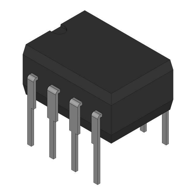
CONNECTION DIAGRAM
8-Lead Plastic Mini-DIP (N)
and SOIC (R) Packages
200k⍀
–IN
+IN
ANALOG
GND
2
–VS
3
G = 30
7
G = 100
6
+VS
5
OUT
100k⍀
FILTER
4
G=2
AD626
range of this amplifier is equal to 6 (+VS – 1 V) which provides a
+24 V CMR while operating from a +5 V supply. Fur thermore,
the AD626 features a CMR of 90 dB typ.
PRODUCT DESCRIPTION
The AD626 is a low cost, true single-supply differential amplifier
designed for amplifying and low-pass filtering small differential
voltages from sources having a large common-mode voltage.
The AD626 can operate from either a single supply of +2.4 V to
+10 V, or dual supplies of ±1.2 V to ±6 V. The input common-mode
The amplifier’s inputs are protected against continuous overload of
up to 50 V, and RFI filters are included in the attenuator network.
The output range is +0.03 V to +4.9 V using a +5 V supply. The
amplifier provides a preset gain of 10, but gains between 10 and
100 can be easily configured with an external resistor. Furthermore, a gain of 100 is available by connecting the G = 100 pin to
analog ground. The AD626 also offers low-pass filter capability by
connecting a capacitor between the filter pin and analog ground.
The AD626A and AD626B operate over the industrial temperature
range of –40°C to +85°C. The AD626 is available in two 8-lead
packages: a plastic mini-DIP and SOIC.
25
120
100
G = 10, 100
VS = +5V
80
G = 100
VS = ⴞ5V
60
40
G = 10
VS = ⴞ5V
20
1
10
100
1k
FREQUENCY – Hz
10k
100k
1M
Figure 1. Common-Mode Rejection vs. Frequency
INPUT COMMON-MODE RANGE – V
140
COMMON-MODE REJECTION – dB
8
1/6
APPLICATIONS
Current Sensing
Interface for Pressure Transducers, Position Indicators,
Strain Gages, and Other Low Level Signal Sources
0
0.1
200k⍀
1
20
ⴞVCM FOR SINGLE
AND DUAL SUPPLIES
15
10
ⴞVCM FOR DUAL
SUPPLIES ONLY
5
0
1
2
3
SUPPLY VOLTAGE – ⴞV
4
5
Figure 2. Input Common-Mode Range vs. Supply
REV. D
Information furnished by Analog Devices is believed to be accurate and
reliable. However, no responsibility is assumed by Analog Devices for its
use, nor for any infringements of patents or other rights of third parties
that may result from its use. No license is granted by implication or otherwise under any patent or patent rights of Analog Devices.Trademarks and
registered trademarks are the property of their respective companies.
One Technology Way, P.O. Box 9106, Norwood, MA 02062-9106, U.S.A.
Tel: 781/329-4700
www.analog.com
Fax: 781/326-8703
© 2003 Analog Devices, Inc. All rights reserved.
�AD626* PRODUCT PAGE QUICK LINKS
Last Content Update: 02/24/2017
COMPARABLE PARTS
REFERENCE MATERIALS
View a parametric search of comparable parts.
Technical Articles
• Auto-Zero Amplifiers
DOCUMENTATION
• High-performance Adder Uses Instrumentation Amplifiers
Application Notes
• AN-244: A User's Guide to I.C. Instrumentation Amplifiers
• Input Filter Prevents Instrumentation-amp RFRectification Errors
• AN-245: Instrumentation Amplifiers Solve Unusual Design
Problems
• The AD8221 - Setting a New Industry Standard for
Instrumentation Amplifiers
• AN-282: Fundamentals of Sampled Data Systems
• AN-589: Ways to Optimize the Performance of a
Difference Amplifier
DESIGN RESOURCES
• AD626 Material Declaration
• AN-671: Reducing RFI Rectification Errors in In-Amp
Circuits
• PCN-PDN Information
Data Sheet
• Symbols and Footprints
• AD626: Low Cost, Single Supply Differential Amplifier
Data Sheet
Technical Books
• A Designer's Guide to Instrumentation Amplifiers, 3rd
Edition, 2006
TOOLS AND SIMULATIONS
• AD626 SPICE Macro-Model
• Quality And Reliability
DISCUSSIONS
View all AD626 EngineerZone Discussions.
SAMPLE AND BUY
Visit the product page to see pricing options.
TECHNICAL SUPPORT
Submit a technical question or find your regional support
number.
DOCUMENT FEEDBACK
Submit feedback for this data sheet.
This page is dynamically generated by Analog Devices, Inc., and inserted into this data sheet. A dynamic change to the content on this page will not
trigger a change to either the revision number or the content of the product data sheet. This dynamic page may be frequently modified.
�AD626–SPECIFICATIONS
SINGLE SUPPLY
(@+VS = +5 V and TA = 25ⴗC, unless otherwise noted.)
Model
Parameter
GAIN
Gain Accuracy
Gain = 10
Gain = 100
Over Temperature, TA = TMIN to TMAX
Gain Linearity
Gain = 10
Gain = 100
OFFSET VOLTAGE
Input Offset Voltage
vs. Temperature
vs. Temperature
vs. Supply Voltage (PSR)
+PSR
–PSR
Condition
Min
Total Error
@ VOUT ≥ 100 mV dc
@ VOUT ≥ 100 mV dc
G = 10
G = 100
@ VOUT ≥ 100 mV dc
@ VOUT ≥ 100 mV dc
RL = 10 k⍀
f = 100 Hz, VCM = +24 V
f = 10 kHz, VCM = +6 V
f = 100 Hz, VCM = –2 V
COMMON-MODE VOLTAGE RANGE
+CMV Gain = 10
–CMV Gain = 10
CMR > 85 dB
CMR > 85 dB
Negative
DYNAMIC RESPONSE
–3 dB Bandwidth
Slew Rate, TMIN to TMAX
Settling Time
POWER SUPPLY
Operating Range
Quiescent Current
TRANSISTOR COUNT
1.0
1.0
50
150
0.2
0.5
0.6
0.6
30
120
%
%
ppm/°C
ppm/°C
0.014
0.014
0.016
0.02
0.014
0.014
0.016
0.02
%
%
1.9
2.5
2.9
6
1.9
2.5
2.9
6
mV
mV
µV/°C
dB
dB
66
55
60
90
64
85
80
55
73
90
64
85
dB
dB
dB
+24
–2
+24
–2
V
V
200
100
6 (VS – l)
200
100
6 (VS – l)
k⍀
k⍀
V
4.90
4.90
V
V
V
V
12
12
mA
2
2
0.25
0.25
2
2
0.25
0.25
µV p-p
µV p-p
µV/冑Hz
µV/冑Hz
100
0.22
0.17
22
kHz
V/µs
V/µs
µs
0.17
0.1
2.4
Number of Transistors
Unit
80
66
f = 0.1 Hz–10 Hz
f = 0.1 Hz–10 Hz
f = 1 kHz
f = 1 kHz
TA = TMIN to TMAX
Gain = 10
Gain = 100
Max
74
64
4.7
4.7
0.03
0.03
VOUT = +1 V dc
Gain = 10
Gain = 100
to 0.01%, 1 V Step
AD626B
Typ
80
66
Short Circuit Current
+ISC
NOISE
Voltage Noise RTI
Gain = 10
Gain = 100
Gain = 10
Gain = 100
Min
74
64
INPUT
Input Resistance
Differential
Common-Mode
Input Voltage Range (Common-Mode)
RL = 10 k⍀
Gain = 10
Gain = 100
Gain = 10
Gain = 100
Max
0.4
0.1
TMIN to TMAX, G = 10 or 100
TMIN to TMAX, G = 10 or 100
COMMON-MODE REJECTION
+CMR Gain = 10, 100
±CMR Gain = 10, 100
–CMR Gain = 10, 100*
OUTPUT
Output Voltage Swing
Positive
AD626A
Typ
4.90
4.90
4.7
4.7
0.03
0.03
100
0.22
0.17
24
5
0.16
0.23
46
0.17
0.1
12
0.20
0.29
2.4
5
0.16
0.23
10
0.20
0.29
V
mA
mA
46
*At temperatures above 25°C, –CMV degrades at the rate of 12 mV/°C; i.e., @ 25°C CMV = –2 V, @ 85°C CMV = –1.28 V.
Specifications subject to change without notice.
–2–
REV. D
�AD626
DUAL SUPPLY
(@+VS = ⴞ5 V and TA = 25ⴗC, unless otherwise noted.)
Model
Parameter
GAIN
Gain Accuracy
Gain = 10
Gain = 100
Over Temperature, TA = TMIN to TMAX
Condition
Min
Total Error
RL = 10 k⍀
TMIN to TMAX, G = 10 or 100
TMIN to TMAX, G = 10 or 100
COMMON-MODE REJECTION
+CMR Gain = 10, 100
±CMR Gain = 10, 100
RL = 10 k⍀
f = 100 Hz, VCM = +24 V
f = 10 kHz, VCM = 6 V
COMMON-MODE VOLTAGE RANGE
+CMV Gain = 10
–CMV Gain = 10
CMR > 85 dB
CMR > 85 dB
RL = 10 k⍀
Gain = 10, 100
Gain = 10
Gain = 100
DYNAMIC RESPONSE
–3 dB Bandwidth
Slew Rate, TMIN to TMAX
Settling Time
POWER SUPPLY
Operating Range
Quiescent Current
TRANSISTOR COUNT
0.1
0.15
0.3
0.6
30
80
%
%
ppm/°C
ppm/°C
0.045
0.01
0.055
0.015
0.045
0.01
0.055
0.015
%
%
50
500
1.0
50
250
0.5
0.5
µV
mV
µV/°C
dB
dB
66
55
90
60
80
55
90
60
dB
dB
26.5
32.5
26.5
32.5
V
V
200
110
6 (VS – l)
200
110
6 (VS – l)
k⍀
k⍀
V
4.90
–2.1
–1.8
V
V
V
12
0.5
12
0.5
mA
mA
2
2
0.25
0.25
2
2
0.25
0.25
µV p-p
µV p-p
µV/冑Hz
µV/冑Hz
100
0.22
0.17
22
kHz
V/µs
V/µs
µs
⫾1.2
4.90
–2.1
–1.8
–3–
4.7
–1.65
–1.45
100
0.22
0.17
24
⫾5
1.5
1.5
46
Specifications subject to change without notice.
REV. D
0.5
1.0
50
100
80
66
0.17
0.1
Number of Transistors
Unit
74
64
f = 0.1 Hz–10 Hz
f = 0.1 Hz–10 Hz
f = 1 kHz
f = 1 kHz
TA = TMIN to TMAX
Gain = 10
Gain = 100
Max
80
66
4.7
–1.65
–1.45
VOUT = +1 V dc
Gain = 10
Gain = 100
to 0.01%, 1 V Step
AD626B
Typ
74
64
Short Circuit Current
+ISC
–ISC
NOISE
Voltage Noise RTI
Gain = 10
Gain = 100
Gain = 10
Gain = 100
Min
1.0
INPUT
Input Resistance
Differential
Common-Mode
Input Voltage Range (Common-Mode)
OUTPUT
Output Voltage Swing
Positive
Negative
Max
0.2
0.25
G = 10
G = 100
Gain Linearity
Gain = 10
Gain = 100
OFFSET VOLTAGE
Input Offset Voltage
vs. Temperature
vs. Temperature
vs. Supply Voltage (PSR)
+PSR
–PSR
AD626A
Typ
0.17
0.1
⫾6
2
2
⫾1.2
⫾5
1.5
1.5
46
⫾6
2
2
V
mA
mA
�AD626
ABSOLUTE MAXIMUM RATINGS1
NOTES
1
Stresses above those listed under Absolute Maximum Ratings may cause permanent
damage to the device. This is a stress rating only; functional operation of the device
at these or any other conditions above those indicated in the operational section of
this specification is not implied. Exposure to absolute maximum rating conditions
for extended periods may affect device reliability.
2
8-Lead Plastic Package: JA = 100°C/W; JC = 50°C/W.
8-Lead SOIC Package: JA = 155°C/W; JC = 40°C/W.
Supply Voltage . . . . . . . . . . . . . . . . . . . . . . . . . . . . . . . . . +36V
Internal Power Dissipation2
Peak Input Voltage . . . . . . . . . . . . . . . . . . . . . . . . . . . . . . +60 V
Maximum Reversed Supply Voltage Limit . . . . . . . . . . . . . –34V
Output Short Circuit Duration . . . . . . . . . . . . . . . . . . Indefinite
Storage Temperature Range (N, R) . . . . . . . . . –65°C to +125°C
Operating Temperature Range
AD626A/AD626B . . . . . . . . . . . . . . . . . . . . –40°C to +85°C
Lead Temperature Range (Soldering 60 sec) . . . . . . . . . +300°C
ORDERING GUIDE
Model
Temperature
Range
Package
Description
Package
Option
AD626AN
AD626AR
AD626BN
AD626AR-REEL
AD626AR-REEL7
–40°C to +85°C
–40°C to +85°C
–40°C to +85°C
–40°C to +85°C
–40°C to +85°C
Plastic DIP
Small Outline IC
Plastic DIP
13" Tape and Reel
7" Tape and Reel
N-8
R-8
N-8
METALLIZATION PHOTOGRAPH
Dimensions shown in inches and (mm).
CAUTION
ESD (electrostatic discharge) sensitive device. Electrostatic charges as high as 4000 V readily accumulate
on the human body and test equipment and can discharge without detection. Although the AD626 features
proprietary ESD protection circuitry, permanent damage may occur on devices subjected to high energy
electrostatic discharges. Therefore, proper ESD precautions are recommended to avoid performance
degradation or loss of functionality.
–4–
REV. D
�Typical Performance Characteristics–AD626
6
VS = ⴞ5V
GAIN = 10, 100
5
POSITIVE OUTPUT VOLTAGE – V
INPUT COMMON-MODE RANGE – V
25
20
ⴞVCM FOR SINGLE
AND DUAL SUPPLIES
15
10
ⴞVCM FOR DUAL
SUPPLIES ONLY
5
0
4
3
2
1
0
–1
1
2
3
4
5
10
100
1k
LOAD RESISTANCE – ⍀
SUPPLY VOLTAGE – ⴞV
TPC 1. Input Common-Mode Range vs. Supply
TPC 4. Positive Output Voltage Swing vs. Resistive Load
–6
TA = 25ⴗC
NEGATIVE OUTPUT VOLTAGE – V
POSITIVE OUTPUT VOLTAGE SWING – V
5
4
SINGLE AND
DUAL SUPPLY
3
2
DUAL SUPPLY
ONLY
1
–5
–4
–3
GAIN = 10
–2
GAIN = 100
–1
0
0
0
1
2
3
SUPPLY VOLTAGE – V
4
1
100
5
TPC 2. Positive Output Voltage Swing vs. Supply Voltage
1k
10k
LOAD RESISTANCE – ⍀
100k
TPC 5. Negative Output Voltage Swing vs. Resistive Load
–5
30
TA = 25ⴗC
CHANGE IN OFFSET VOLTAGE – V
NEGATIVE OUTPUT VOLTAGE SWING – V
10k
–4
–3
DUAL SUPPLY
ONLY
–2
–1
0
0
1
2
3
SUPPLY VOLTAGE – V
4
20
10
0
5
0
1
2
3
4
5
WARM-UP TIME – Minutes
TPC 3. Negative Output Voltage Swing vs. Supply Voltage
REV. D
TPC 6. Change in Input Offset Voltage vs. Warm-Up Time
–5–
�AD626
100
COMMON-MODE REJECTION – dB
1000
VS = ⴞ5V
DUAL SUPPLY
CLOSED-LOOP GAIN
GAIN = 100
100
VS = +5V
SINGLE SUPPLY
GAIN = 10
10
VS = ⴞ5V
DUAL SUPPLY
0
10
100
90
85
80
VS = ⴞ5
75
70
1k
10k
FREQUENCY – Hz
100k
65
20
1M
TPC 7. Closed-Loop Gain vs. Frequency
22
24
26
28
INPUT COMMON-MODE VOLTAGE – V
30
TPC 10. Common-Mode Rejection vs. Input
Common- Mode Voltage for Dual-Supply Operation
100
140
COMMON-MODE REJECTION – dB
120
COMMON-MODE REJECTION – dB
95
100
G = 10, 100
VS = +5
80
G = 100
VS = ⴞ5
60
40
G = 10
VS = ⴞ5
G = 10, 100
90
80
70
20
0
0.1
60
1
10
100
1k
FREQUENCY – Hz
10k
100k
1M
0
TPC 8. Common-Mode Rejection vs. Frequency
60
80
0.7
G = 10, 100
95
CURVE APPLIES TO
ALL SUPPLY VOLTAGES
AND GAINS BETWEEN 10 AND 100
0.6
ADDITIONAL GAIN ERROR – %
COMMON-MODE REJECTION – dB
40
TPC 11. Common-Mode Rejection vs. Input Source
Resistance Mismatch
100
90
85
80
VS = +5
75
70
65
–5
20
INPUT SOURCE RESISTANCE MISMATCH – ⍀
0.5
TOTAL GAIN ERROR =
GAIN ACCURACY (FROM SPEC TABLE)
+ ADDITIONAL GAIN ERROR
0.4
0.3
0.2
0.1
0
5
10
15
20
INPUT COMMON-MODE VOLTAGE – V
0.0
25
10
TPC 9. Common-Mode Rejection vs. Input CommonMode Voltage for Single-Supply Operation
100
SOURCE RESISTANCE MISMATCH – ⍀
1k
TPC 12. Additional Gain Error vs. Source
Resistance Mismatch
–6–
REV. D
�AD626
2V PER VERTICAL DIVISION
QUIESCENT CURRENT – mA
0.16
0.15
G = 10
0.14
0.13
0.12
1
2
3
SUPPLY VOLTAGE – V
4
5
5 SECONDS PER HORIZONTAL DIVISION
TPC 13. Quiescent Supply Current vs. Supply Voltage
for Single-Supply Operation
TPC 16. 0.1 Hz to 10 Hz RTI Voltage Noise. VS = ±5 V,
Gain = 100
100
80
1.5
CLOSED-LOOP GAIN
QUIESCENT CURRENT – mA
2.0
1.0
FOR VS = ⴞ5V AND +5V
60
40
0.5
20
0
ⴞ1
ⴞ2
ⴞ3
SUPPLY VOLTAGE – V
ⴞ4
0
ⴞ5
1
TPC 14. Quiescent Supply Current vs. Supply Voltage
for Dual-Supply Operation
POWER SUPPLY REJECTION – dB
Hz
VOLTAGE NSD – V/
100k
1M
140
1.0
GAIN = 10, 100
0.1
VS = ⴞ5V DUAL SUPPLY
1
10
100
1k
FREQUENCY – Hz
10k
ALL CURVES FOR
GAINS OF 10 OR 100
120
100
SINGLE AND DUAL
–PSRR
80
60
SINGLE
+PSRR
40
20
0.1
100k
TPC 15. Noise Voltage Spectral Density vs. Frequency
REV. D
100
1k
10k
VALUE OF RESISTOR RG – ⍀
TPC 17. Closed-Loop Gain vs. RG
10
0.01
10
DUAL
DUAL
+PSRR
+PSRR
1
10
100
1k
FREQUENCY – Hz
10k
100k
1M
TPC 18. Power Supply Rejection vs. Frequency
–7–
�AD626
100
100
90
90
10
10
0%
0%
TPC 19. Large Signal Pulse Response. VS = ±5 V, G = 10
TPC 22. Large Signal Pulse Response. VS = +5 V, G = 100
100
100
90
90
10
10
0%
0%
TPC 20. Large Signal Pulse Response. VS = ±5 V, G = 100
TPC 23. Settling Time. VS = ±5 V, G = 10
500mV
100
100
90
90
10
10
0%
0%
TPC 21. Large Signal Pulse Response. VS = +5 V, G = 10
TPC 24. Settling Time. VS = ±5 V, G = 100
–8–
REV. D
�AD626
100
100
90
90
10
10
0%
0%
TPC 25. Settling Time. VS = +5 V, G = 10
TPC 26. Settling Time. VS = +5 V, G = 100
Figure 4 shows the main elements of the AD626. The signal inputs
at Pins 1 and 8 are first applied to dual resistive attenuators R1
through R4 whose purpose is to reduce the peak common-mode
voltage at the input to the preamplifier—a feedback stage based
on the very low drift op amp A1. This allows the differential
input voltage to be accurately amplified in the presence of large
common-mode voltages six times greater than that which can be
tolerated by the actual input to A1. As a result, the input CMR
extends to six times the quantity (VS – 1 V). The overall commonmode error is minimized by precise laser-trimming of R3 and R4,
thus giving the AD626 a common-mode rejection ratio (CMRR)
of at least 10,000:1 (80 dB).
ERROR
OUT
10k⍀
10k⍀
2k⍀
+VS
INPUT
20V p–p
10k⍀
AD626
1k⍀
–VS
Figure 3. Settling Time Test Circuit
To minimize the effect of spurious RF signals at the inputs due to
rectification at the input to A1, small filter capacitors C1 and C2
are included.
THEORY OF OPERATION
The AD626 is a differential amplifier consisting of a precision
balanced attenuator, a very low drift preamplifier (A1), and an
output buffer amplifier (A2). It has been designed so that small
differential signals can be accurately amplified and filtered in the
presence of large common-mode voltages (VCM), without the use
of any other active components.
The output of A1 is connected to the input of A2 via a 100 k⍀
(R12) resistor to facilitate the low-pass filtering of the signal of
interest (see Low-Pass Filtering section).
The 200 k⍀ input impedance of the AD626 requires that the source
resistance driving this amplifier be low in value (