14-Bit, 92.16 MSPS, 4-/6-Channel
Wideband IF to Baseband Receiver
AD6654
FEATURES
APPLICATIONS
SNR = 90 dB in 1.25 MHz bandwidth to Nyquist
SNR = 87 dB in 1.25 MHz bandwidth to 200 MHz
Integrated 14-bit, 92.16 MSPS ADC
IF sampling frequencies to 200 MHz
Internal 2.4 V reference, 2.2 V p-p analog input range
Internal differential track-and-hold analog input
Processes 4/6 wideband carriers simultaneously
Fractional clock multiplier to 200 MHz
Programmable decimating FIR filters, interpolating
half-band filters and programmable AGC loops
with 96 dB range
Three 16-bit configurable parallel output ports
User-configurable built-in self-test (BIST) capability
8-/16-bit microport and SPORT/SPI® serial port control
Multicarrier, multimode digital receivers
GSM, EDGE, PHS, UMTS, WCDMA, CDMA2000,
TD-SCDMA, WiMAX
Micro and pico cell systems, software radios
Wireless local loop
Smart antenna systems
In-building wireless telephony
Broadband data applications
Instrumentation and test equipment
FUNCTIONAL BLOCK DIAGRAM
FIR1
HB1
M = BYP, 2
FIR2
HB2
M = BYP, 2
MRCF
DRCF
M = 1–16
CRCF
M = 1–16
LHB
L = 1, 2
NCO
CIC5
M = 1–32
FIR1
HB1
M = BYP, 2
FIR2
HB2
M = BYP, 2
MRCF
DRCF
M = 1–16
SHA
ADC
CRCF
M = 1–16
LHB
L = 1, 2
NCO
CIC5
M = 1–32
FIR1
HB1
M = BYP, 2
FIR2
HB2
M = BYP, 2
MRCF
DRCF
M = 1–16
CRCF
M = 1–16
LHB
L = 1, 2
NCO
CIC5
M = 1–32
FIR1
HB1
M = BYP, 2
FIR2
HB2
M = BYP, 2
MRCF
DRCF
M = 1–16
CRCF
M = 1–16
LHB
L = 1, 2
NCO
CIC5
M = 1–32
FIR1
HB1
M = BYP, 2
FIR2
HB2
M = BYP, 2
MRCF
DRCF
M = 1–16
CRCF
M = 1–16
LHB
L = 1, 2
NCO
CIC5
M = 1–32
FIR1
HB1
M = BYP, 2
FIR2
HB2
M = BYP, 2
MRCF
DRCF
M = 1–16
CRCF
M = 1–16
LHB
L = 1, 2
INPUT
MATRIX
2.4V
VREF
PRN
GEN
OVR
(ADC OVERRANGE)
EXP
(VGA LEVEL CONTROL)
3
EXP
BITS
PEAK/
RMS
MSMT
(AVAILABLE IN
6-CHANNEL MODEL ONLY)
M = DECIMATION
L = INTERPOLATION
AVDD, DRVDD,
VDDCORE, VDDIO, GND
SYNC
0, 1, 2, 3
CLOCK
MULTIPLIER
AGC
8-BIT/16-BIT MICROPORT
INTERFACE
PARALLEL PORTS
14
AIN–
VREF
CIC5
M = 1–32
SPORT/
SPI INTERFACE
PA
PB
PC
05156-001
ENC–
AIN+
NCO
INTERNAL
TIMING
DATA ROUTER MATRIX
ENC+
DATA ROUTING
4-CHANNEL AND 6-CHANNEL DIGITAL DOWN CONVERTER
14-BIT ADC FRONT END
Figure 1.
Rev. 0
Information furnished by Analog Devices is believed to be accurate and reliable.
However, no responsibility is assumed by Analog Devices for its use, nor for any
infringements of patents or other rights of third parties that may result from its use.
Specifications subject to change without notice. No license is granted by implication
or otherwise under any patent or patent rights of Analog Devices. Trademarks and
registered trademarks are the property of their respective owners.
One Technology Way, P.O. Box 9106, Norwood, MA 02062-9106, U.S.A.
Tel: 781.329.4700
www.analog.com
Fax: 781.461.3113
©2005 Analog Devices, Inc. All rights reserved.
�AD6654
TABLE OF CONTENTS
General Description ......................................................................... 4
Input Crossbar Matrix ............................................................... 33
Product Highlights ....................................................................... 5
Numerically Controlled Oscillator (NCO) ................................. 34
Specifications..................................................................................... 6
NCO Frequency.......................................................................... 34
Recommended Operating Conditions ...................................... 6
Mixer............................................................................................ 35
ADC DC Specifications ............................................................... 6
Bypass .......................................................................................... 35
ADC Digital Specifications ......................................................... 6
Clear Phase Accumulator on Hop ........................................... 35
ADC Switching Specifications.................................................... 7
Phase Dither................................................................................ 35
ADC AC Specifications ............................................................... 7
Amplitude Dither ....................................................................... 35
Electrical Characteristics............................................................. 8
NCO Frequency Hold-Off Register......................................... 35
Timing Characteristics ................................................................ 9
Phase Offset................................................................................. 35
Microport Timing Characteristics ........................................... 10
HOP Sync .................................................................................... 35
Serial Port Timing Characteristics ........................................... 11
Fifth-Order CIC Filter ................................................................... 36
Timing Diagrams............................................................................ 12
Bypass .......................................................................................... 36
Absolute Maximum Ratings.......................................................... 18
CIC Rejection.............................................................................. 36
Thermal Characteristics ............................................................ 18
Example Calculations ................................................................ 37
Explanation of Test Levels ......................................................... 18
FIR Half-Band Block...................................................................... 38
ESD Caution................................................................................ 18
3-Tap Fixed coefficient Filter (FIR1) ....................................... 38
Pin Configuration and Function Descriptions........................... 19
Decimate-by-2 Half-Band Filter (HB1) .................................. 38
Typical Performance Characteristics ........................................... 22
6-Tap Fixed Coefficient Filter (FIR2) ...................................... 39
ADC Equivalent Circuits............................................................... 25
Decimate-by-2 Half-Band Filter (HB2) .................................. 39
Terminology .................................................................................... 26
Intermediate Data Router.............................................................. 41
Theory of Operation ...................................................................... 27
Mono-Rate RAM Coefficient Filter (MRCF) ............................. 42
ADC Architecture ...................................................................... 27
Symmetry .................................................................................... 42
Application information ................................................................ 28
Clock Rate ................................................................................... 42
ADC Configuration Notes ........................................................ 28
Bypass .......................................................................................... 42
DDC Configuration Notes ........................................................ 29
Scaling.......................................................................................... 42
ADC Input Port Monitor Function.............................................. 31
Decimating RAM Coefficient Filter (DRCF) ............................. 43
Peak Detector Mode................................................................... 31
Bypass .......................................................................................... 43
Mean Power Mode ..................................................................... 31
Scaling.......................................................................................... 43
Threshold Crossing Mode......................................................... 32
Symmetry .................................................................................... 43
Additional Control Bits ............................................................. 32
Coefficient Offset ....................................................................... 43
Rev. 0 | Page 2 of 88
�AD6654
Decimation Phase .......................................................................43
HOP ..............................................................................................58
Maximum Number of Taps Calculated....................................43
Serial Port Control ..........................................................................60
Programming DRCF Registers for
an Asymmetrical Filter ...............................................................44
Hardware Interface .....................................................................60
Programming DRCF Registers for a Symmetric Filter ..........44
Channel RAM Coefficient Filter (CRCF) ....................................45
SPI Mode Timing........................................................................62
SPORT Mode Timing.................................................................64
Bypass ...........................................................................................45
Programming Indirect Addressed Registers
Using Serial Port..........................................................................67
Scaling...........................................................................................45
Connecting the AD6654 Serial Port to a Blackfin DSP .........69
Symmetry .....................................................................................45
Microport .........................................................................................70
Coefficient Offset ........................................................................45
Intel (Inm) Mode ........................................................................70
Decimation Phase .......................................................................45
Motorola (MNM) Mode ............................................................70
Maximum Number of TAPS Calculated..................................45
Accessing Multiple AD6654 Devices .......................................71
Programming CRCF Registers for an
Asymmetrical Filter ....................................................................46
Memory Map ...................................................................................72
Programming CRCF Registers for a Symmetrical Filter .......46
Interpolating Half-Band Filter.......................................................47
Output Data Router ........................................................................48
Interleaving Data.........................................................................48
Automatic Gain Control.................................................................49
AGC Loop ....................................................................................49
Desired Signal Level Mode ........................................................50
Desired Clipping Level Mode....................................................52
AGC Synchronization.................................................................52
SYNC Process ..............................................................................52
Parallel Port Output ........................................................................53
Interleaved I/Q Mode .................................................................53
Reading the Memory Map Table...............................................72
Bit Format ....................................................................................72
Open Locations ...........................................................................72
Default Values..............................................................................72
Logic Levels..................................................................................72
Global Register Map ...................................................................74
Input Port Register Map.............................................................76
Channel Register Map ................................................................78
MRCF Coefficient Memory.......................................................79
Output Port Register Map..........................................................82
DDC Design Notes .........................................................................85
Outline Dimensions........................................................................87
Ordering Guide ...........................................................................87
Parallel IQ Mode .........................................................................53
Master/Slave PCLK Modes ........................................................55
Parallel Port Pin Functions ........................................................56
REVISION HISTORY
4/05—Revision 0: Initial Version
User-Configurable Built-In Self-Test (BIST)...............................57
Chip Synchronization .....................................................................58
Start ...............................................................................................58
Rev. 0 | Page 3 of 88
�AD6654
GENERAL DESCRIPTION
The AD6654 is a mixed-signal IF-to-baseband receiver
consisting of a 14-bit, 92.16 MSPS analog-to-digital converter
(ADC) and a 4-/6-channel, multimode digital down-converter
(DDC) capable of processing up to six WCDMA (wideband
code division multiple access) channels. The AD6654 has been
optimized for the demanding filtering requirements of wideband standards such as CDMA2000, UMTS, and TD-SCDMA,
but is flexible enough to support wider standards such as
WiMAX. It is typically used as part of a radio system that
digitally demodulates and filters IF sampled signals.
The ADC stage features a high performance track-and-hold
input amplifier (T/H), integrated voltage reference, and 14-bit
sampling resolution. Input signals up to 200 MHz can be
accurately digitized at encode rates up to 92.16 MSPS. The ADC
data outputs are internally routed directly into the DDC inputs,
where down-conversion, decimation and digital filtering are
performed. An overrange (OVR) output bit provides indication
of excessive ADC input levels. An ADC data-ready (DR) output
bit provides a synchronized clock for the integrated DDC.
Data from the ADC is evaluated for peak or mean power in the
input stage of the DDC, and the result is available to the user via
control register access. The DDC input stage also outputs 3-bit
level-indicator data (EXP) bits that can be used to control the
gain of the external DVGA in 6 dB steps (up to 48 dB) to
optimize signal amplitude into the ADC input.
The DDC stage has the following signal processing stages: six
WCDMA-ready channels, each consisting of a frequency
translator, a fifth-order cascaded integrated comb filter, two sets
of cascaded fixed coefficient FIR and half-band filters, three
cascaded programmable sum of product FIR filters, an
interpolating half-band filter (IHB), and a digital automatic
gain control (AGC) block. Multiple modes are supported for
clocking data out of the chip. Programming is accomplished via
serial or microport interfaces.
Frequency translation is accomplished with a 32-bit complex
numerically controlled oscillator (NCO). The NCO has greater
than 110 dBc SDFR. This stage translates a real input signal
from an intermediate frequency (IF) to a baseband complex
digital output. Phase and amplitude dither can be enabled onchip to improve spurious performance of the NCO. A 16-bit
phase-offset word is available to create a known phase relationship between multiple AD6654 chips or channels. The NCO can
also be bypassed.
Following frequency translation is a fifth-order CIC filter with a
programmable decimation between 1 and 32. This filter is used
to efficiently lower the sample rate, while providing sufficient
alias rejection at frequencies at higher offsets from the signal
of interest.
Following the CIC5 are two sets of filters. Each filter set
includes a nondecimating FIR filter and a decimate-by-2 halfband filter. The FIR1 filter provides about 30 dB of rejection,
while the HB1 provides about 77 dB of rejection. These two sets
of filters can be used together to achieve a 107 dB stop-band
alias rejection, or they can be individually bypassed to save
power.
The FIR2 filter provides about 30 dB of rejection, while the HB2
filter provides about 65 dB of rejection. The filters can be used
together to achieve more than 95 dB stop-band alias rejection,
or they can be individually bypassed to save power. FIR1 and
HB1 filters can run at the maximum ADC data port rate. In
contrast, FIR2 and HB2 can run with a maximum input rate of
75 MSPS (input rate to FIR2 and HB2 filters).
The programmable filtering is divided into three cascaded RAM
coefficient filters (RCFs) for flexible and power-efficient
filtering. The first filter in the cascade is the MRCF, consisting
of a programmable nondecimating FIR. It is followed by
programmable FIR filters (DRCF) with decimation from 1 to
16. They can be used either together to provide high rejection
filters, or independently to save power. The maximum input
rate to the MRCF is one-fourth the PLL clock rate.
The CRCF (Channel RCF) is the last programmable FIR filter
with programmable decimation from 1 to 16. It is typically used
to meet the spectral mask requirements for the air standard of
interest. This could be an RRC, antialiasing filter or any other
real data filter. Decimation in preceding blocks is used to keep
the input rate of this stage as low as possible for the best filter
performance.
The last filter stage in the chain is an interpolate-by-2 half-band
filter, which is used to up-sample the CRCF output to produce
higher output oversampling. Signal rejection requirements for
this stage are relaxed, because preceding filters have already
filtered the blockers and adjacent carriers.
The DDC input port of the AD6654 has its own clock input
used for latching the input data, as well as for providing the
input for an onboard PLL clock multiplier. The output of the
PLL clock is used for processing all filters and processing blocks
beyond the data router following CIC filter. The PLL clock can
be programmed to have a maximum clock rate of 200 MHz.
Typically, the DDC input clock is driven directly from the
integrated ADC’s data-ready (DR) output to ensure proper
synchronization.
A data routing block is used to distribute data from the CICs to
the various channel filters. This block allows multiple back-end
filter chains to work together to process high bandwidth signals
or to make even sharper filter transitions than a single channel
Rev. 0 | Page 4 of 88
�AD6654
can perform. It can also allow complex filtering operations to be
achieved in the programmable filters.
The digital AGC provides the user with scaled digital outputs
based on the rms level of the signal present at the output of the
digital filters. The user can set the requested level and time
constant of the AGC loop for optimum performance of the
postprocessor. This is a critical function in the base station for
CDMA application, where the power level must be well
controlled going into the RAKE receivers. It has programmable
clipping and rounding control to provide different output
resolutions.
The overall filter response for the AD6654 is the composite of
all the combined filter stages. Each successive filter stage is
capable of narrower transition bandwidths, but requires a
greater number of CLK cycles to calculate the output. The
AD6654 features a fractional clock multiplier that uses the ADC
clock (which is slower than the DDC’s processing speed) to
produce a DDC master clock up to 200 MHz. This feature
allows fractional multiplication of the input clock to allow the
DDC to function at maximum speed while maintaining edge
identity to the ADC clock.
More decimation in the first filter stage minimizes overall
power consumption. Data from the device is interfaced to a
DSP/FPGA/baseband processor via high speed parallel ports
(preferred), or a DSP-compatible microprocessor interface.
The AD6654 is available in 4-channel and 6-channel versions.
The primary focus of the data sheet is on the 6-channel part.
The only difference between the 6-channel and 4-channel
devices is that, on the 4-channel version, Channel 4 and
Channel 5 are not available (see Figure 1). The 4-channel device
has the same DDC input port features, output ports, and
memory map as the 6-channel device. On the 4-channel
version, the memory map section for Channel 4 and Channel 5
can be programmed and read back, but the two extra channels
are disabled internally.
PRODUCT HIGHLIGHTS
1.
Integrated 14-bit, 92.16 MSPS ADC.
2.
Track-and-hold amplifier analog input for excellent IF
sampling up to 200 MHz.
3.
Four or six independent digital filtering channels.
4.
RMS/peak power monitoring of the ADC data port and
96 dB range AGCs before the output ports.
5.
Three programmable RAM coefficient filters, three halfband filters, two fixed coefficient filters, and one fifthorder CIC filter per channel.
6.
Complex filtering by combining filtering capability of
multiple channels.
7.
Three 16-bit parallel output ports operating at up to
200 MHz clock.
8.
Blackfin®- and TigerSHARC®-compatible, 8-/16-bit
microprocessor port.
9.
Synchronous serial communications port is compatible
with most serial interface standards: SPORT, SPI, and SSR.
Rev. 0 | Page 5 of 88
�AD6654
SPECIFICATIONS
RECOMMENDED OPERATING CONDITIONS
Table 1.
Parameter (Conditions)
AVDD1
DRVDD2
VDDCORE
VDDIO2
TAMBIENT
Temp
Full
Full
Full
Full
1
Specified for dc supplies with linear rise-time B
DECREASE
EXTERNAL GAIN
DEC
INCREASE
EXTERNAL GAIN
COMPARE
AB
These functions are controlled via the 2-bit power monitor
function select bits in the power monitor control register of the
DDC input port. The DDC input port can be set for different
modes, but only one function can be active at a time. The three
modes of operation can function continuously over a programmable time period. This time period is programmed as the
number of input clock cycles in a 24-bit ADC monitor period
register (AMPR). An internal magnitude storage register (MSR)
is used to monitor, accumulate, or count, depending on the
mode of operation.
PEAK DETECTOR MODE
Control Bits 00
The magnitude of the input port signal is monitored over a
programmable time period (given by AMPR) to give the peak
value detected. This mode is set by programming Logic 0 in the
power monitor function select bits in the power monitor
control register of the DDC input port. The 24-bit AMPR must
be programmed before activating this mode.
After enabling this mode, the value in the AMPR is loaded into
a monitor period timer and the countdown is started. The
magnitude of the input signal is compared to the MSR, and the
greater of the two is updated back into the MSR. The initial
value of the MSR is set to the current ADC input signal magnitude. This comparison continues until the monitor period timer
reaches a count of 1.
When the monitor period timer reaches a count of 1, the value
in the MSR is transferred to the power monitor holding register,
which can be read through the microport or the serial port. The
monitor period timer is reloaded with the value in the AMPR,
and the countdown is started. Also, the magnitude of the first
input sample is updated in the MSR, and the comparison and
update procedure, as explained above, continues. If the
interrupt is enabled, an interrupt is generated, and the interrupt
status register is updated when the AMPR reaches a count of 1.
05156-033
The AD6654 provides a power monitor function that can
monitor the DDC input stream and gather statistics about the
received signal in a signal chain. This function block can
operate in one of three modes measuring the following over a
programmable period of time:
Figure 44. ADC Input Peak Detector Block Diagram
MEAN POWER MODE
Control Bits 01
In this mode, the magnitude of the input port signal is
integrated (by adding an accumulator) over a programmable
time period (given by AMPR) to give the integrated magnitude
of the input signal. This mode is set by programming Logic 1 in
the power monitor function select bits in the power monitor
control register of the DDC input port. The 24-bit AMPR,
representing the period over which integration is performed,
must be programmed before activating this mode.
After enabling this mode, the value in the AMPR is loaded into
a monitor period timer, and the countdown is immediately
started. The 15-bit magnitude of input signal is right-shifted by
nine bits to give 6-bit data. This 6-bit data is added to the
contents of a 24-bit holding register, thereby performing an
accumulation. The integration continues until the monitor
period timer reaches a count of 1.
When the monitor period timer reaches a count of 1, the value
in the MSR is transferred to the power monitor holding register
(after some formatting), which can be read through the microport or the serial port. The monitor period timer is reloaded
with the value in the AMPR, and the countdown is started.
Also, the first input sample signal magnitude is updated in the
MSR, and the accumulation continues with the subsequent
input samples. If the interrupt is enabled, an interrupt is
generated, and the interrupt status register is updated when the
AMPR reaches a count of 1. Figure 45 illustrates the mean
power monitoring logic.
The value in the MSR is a floating-point number with 4 MSBs
and 20 LSBs. If the 4 MSBs are EXP and the 20 LSBs are MAG,
the value in dBFS can be decoded using the following equation:
Figure 44 is a block diagram of the peak detector logic. The
MSR contains the absolute magnitude of the peak detected by
the peak detector logic.
Rev. 0 | Page 31 of 88
⎡⎛ MAG ⎞
⎤
MeanPower = 10 log ⎢⎜ 20 ⎟2 − (EXP − 1)⎥
⎠
⎣⎝ 2
⎦
�AD6654
FROM
MEMORY
MAP
POWER MONITOR
PERIOD REGISTER
DOWN
COUNTER
IS COUNT = 1?
TO
INTERRUPT
CONTROLLER
LOAD
CLEAR
LOAD
POWER MONITOR
HOLDING
REGISTER
ACCUMULATOR
TO
MEMORY
MAP
05156-034
FROM
INPUT
PORTS
Figure 45. ADC Input Mean Power Monitoring Block Diagram
THRESHOLD CROSSING MODE
Control Bits 10
In this mode of operation, the magnitude of the input port
signal is monitored over a programmable time period (given
by AMPR) to count the number of times it crosses a certain
programmable threshold value. This mode is set by programming Logic 1x (where x is a don’t care bit) in the power monitor
function select bits in the power monitor control register of the
DDC input port. Before activating this mode, the user needs to
program the 24-bit AMPR and the 10-bit upper threshold register
of the DDC input port. The same upper threshold register is
used for both power monitoring and gain control (see the ADC
Gain Control section).
After entering this mode, the value in the AMPR is loaded into
a monitor period timer, and the countdown is started. The
magnitude of the input signal is compared to the upper
threshold register (programmed previously) on each input clock
cycle. If the input signal has a magnitude greater than the upper
threshold register, then the MSR register is incremented by 1.
The initial value of the MSR is set to 0. This comparison and
incrementing of the MSR register continues until the monitor
period timer reaches a count of 1.
When the monitor period timer reaches a count of 1, the value
in the MSR is transferred to the power monitor holding register,
which can be read through the microport or the serial port. The
monitor period timer is reloaded with the value in the AMPR,
and the countdown is started. The MSR register is also cleared
to a value of 0. If interrupts are enabled, an interrupt is generated, and the interrupt status register is updated when the
AMPR reaches a count of 1. Figure 46 illustrates the threshold
crossing logic. The value in the MSR is the number of samples
that have an amplitude greater than the threshold register.
FROM
MEMORY
MAP
POWER MONITOR
PERIOD REGISTER
DOWN
COUNTER
IS COUNT = 1?
TO
INTERRUPT
CONTROLLER
ADDITIONAL CONTROL BITS
For additional flexibility in the power monitoring process, two
control bits are provided in the power monitor control register.
The two control bits are the disable monitor period timer bit
and the clear-on-read bit. These options have the same function
in all three modes of operation.
Disable Monitor Period Timer Bit
When the disable monitor period timer bit is written with
Logic 1, the timer continues to run but does not cause the
contents of the MSR to be transferred to the holding register
when the count reaches 1. This function of transferring the
MSR to the power monitor holding register and resetting the
MSR is now controlled by a read operation on the microport or
serial port.
When a microport or serial port read is performed on the
power monitor holding register, the MSR value is transferred to
the holding register. After the read operation, the timer is
reloaded with the AMPR value. If the timer reaches 1 before the
microport or serial port read, the MSR value is not transferred
to the holding register, as in normal operation. The timer still
generates an interrupt on the AD6654 interrupt pin and updates
the interrupt status register. An interrupt appears on the IRP
pin, if interrupts are enabled in the interrupt enable register.
Clear-on-Read Bit
This control bit is valid only when the disable monitor period
timer bit is Logic 1. When both of these bits are set, a read
operation to either the microport or the serial port reads the
MSR value, and the monitor period timer is reloaded with the
AMPR value. The MSR is cleared (written with current input
signal magnitude in peak power and mean power modes;
written with a 0 in threshold crossing mode), and normal
operation continues.
When the monitor period timer is disabled and the clear-onread bit is set, a read operation to the power monitor holding
register clears the contents of the MSR and, therefore, the power
monitor loop restarts.
If the clear-on-read bit is Logic 0, the read operation to the
microport or serial port does not clear the MSR value after it is
transferred into the holding register. The value from the
previous monitor time period persists, and it continues to be
compared, accumulated, or incremented, based on new input
signal magnitude values.
LOAD
FROM
MEMORY
MAP
CLEAR
A COMPARE
A>B
COMPARE
A>B
LOAD
POWER MONITOR
HOLDING
REGISTER
TO
MEMORY
MAP
B
UPPER
THRESHOLD
REGISTER
05156-035
FROM
INPUT
PORTS
Figure 46. ADC Input Threshold Crossing Block Diagram
Rev. 0 | Page 32 of 88
�AD6654
INPUT CROSSBAR MATRIX
The AD6654 has one ADC input port and six channels. Each
channel can individually select its input source from either the
real ADC input port, or from an internally generated pseudo
random sequence (referred to as a PN sequence) generator.
Each channel has an input crossbar matrix to facilitate selection
of the input signal source.
Each channel has a separate selection for individual control.
Cross bar mux selection enables each channel to select its input
signal source.
The selection of input signal for a particular channel is made
using a 4-bit cross bar mux select word in the ADC input
control register.
Table 14. Cross Bar Mux Selection Bits
Table 14 gives the valid combinations of cross bar mux select
values and the corresponding input signal selections.
Cross Bar Mux Select Bits
0010
0100
Rev. 0 | Page 33 of 88
Input Signal Selection
ADC input drives the channel.
Internal PN sequence drives the
channel.
�AD6654
NUMERICALLY CONTROLLED OSCILLATOR (NCO)
Each channel consists of an independent complex NCO and a
complex mixer. This processing stage is comprised of a digital
tuner consisting of three multipliers and a 32-bit complex NCO.
The NCO serves as a quadrature local oscillator capable of
producing an NCO frequency of between –CLK/2 and +CLK/2
with a resolution of CLK/232 in the complex mode, where CLK
is the input clock frequency.
The NCO frequency word can be calculated using following the
equation:
The frequency word used for generating the NCO is a 32-bit
word. This word is used to generate a 20-bit phase word. A
16-bit phase offset word is added to this phase word. 18 bits of
this phase word are used to generate the sine and cosine of the
required NCO frequency. The amplitude of the sine and cosine
are represented using 17 bits. The worst-case spurious signal
from the NCO is better than −100 dBc for all output
frequencies.
NCO_FREQ is the 32-bit twos complement number representing the NCO frequency register.
Because all the filtering in the AD6654 is low-pass filtering, the
carrier of interest is tuned down to dc (frequency = 0 Hz). This
is illustrated in Figure 47. Once the signal of interest is tuned
down to dc, the unwanted adjacent carriers can be rejected
using the low-pass filtering that follows.
Note that this equation applies to the aliasing of signals in the
digital domain (that is, aliasing introduced when digitizing
analog signals).
NCO _ FREQ = 2 32
mod ( f CH , f CLK )
f CLK
where:
fCH is the desired carrier frequency.
fCLK is the clock rate for the channel under consideration.
mod( ) is a remainder function. For example, mod(110, 100) =
10 and, for negative numbers, mod(−32, 10) = −2.
For example, if the carrier frequency is 100 MHz and the clock
frequency is 80 MHz,
mod ( f CH , f DK )
NCO FREQUENCY
The NCO frequency value is given by the 32-bit twos complement number entered in the NCO frequency register.
Frequencies between −CLK/2 and +CLK/2 (with +CLK/2
excluded) are represented using this frequency word:
f CLK
=
20
= 0.25
80
This, in turn, converts to 0x4000 0000 in the 32-bit twos
complement representation for NCO_FREQ.
0x8000 0000 represents a frequency given by −CLK/2.
0x0000 0000 represents dc (frequency is 0 Hz).
0x7FFF FFFF represents CLK/2 − CLK/232.
WIDEBAND INPUT SPECTRUM (–fsample/2 TO +fsample/2)
SIGNAL OF INTEREST IMAGE
–fs/2
–7fs/16
–3fs/8
–5fs/16
SIGNAL OF INTEREST
–fs/4
–3fs/16
–fs/8
–fs/16
DC
fs/16
fs/8
3fs/16
fs/4
5fs/16
3fs/8
7fs/16
fs/2
5fs/16
3fs/8
7fs/16
fs/2
WIDEBAND INPUT SPECTRUM (30MHz FROM HIGH SPEED ADC)
NCO TUNES SIGNAL TO
–fs/2
–7fs/16
–3fs/8
–5fs/16
–fs/4
–3fs/16
–fs/8
–fs/16
DC
SIGNAL OF INTEREST IMAGE
fs/16
fs/8
3fs/16
fs/4
FREQUENCY TRANSLATION (SINGLE 1MHz CHANNEL TUNED TO BASEBAND)
Figure 47. Frequency Translation Principle Using the NCO and Mixer
Rev. 0 | Page 34 of 88
05156-036
SIGNAL OF INTEREST
AFTER FREQUENCY TRANSLATION
�AD6654
If the carrier frequency is 70 MHz and the clock frequency is
80 MHz, then:
mod( f CH , f CLK ) 10
=
= 0.125
80
f CLK
This, in turn, converts to 0xE000 0000 in the twos complement
32-bit representation.
MIXER
The NCO is accompanied by a mixer. Its operation is similar to
an analog mixer. It performs the down-conversion of real input
signals by using the NCO frequency as a local oscillator. This
mixer performs a real mixer operation (with two multipliers).
The mixer adjusts its operation based on the input signal
provided to each individual channel.
BYPASS
The NCO and the mixer can be individually bypassed in each
channel by writing Logic 1 in the NCO bypass bit in the NCO
control register of the channel under consideration.
CLEAR PHASE ACCUMULATOR ON HOP
When clear, the NCO accumulator bit of the NCO control
register is set (Logic 1), the NCO phase accumulator is cleared
prior to a frequency hop. Refer to the Chip Synchronization
section for details on frequency hopping. This ensures a
consistent phase of the NCO on each hop. The NCO phase
offset is unaffected by this setting and is still in effect. If phasecontinuous hopping is needed, this bit should be cleared (NCO
accumulator is not cleared). The last phase in the NCO phase
register is the initiating point for the new frequency.
PHASE DITHER
The AD6654 provides a phase dither option for improving the
spurious performance of the NCO. Writing Logic 1 in the phase
dither enable bit of the NCO control register of individual
channels enables phase dither. When phase dither is enabled,
random phase is added to the LSBs of the phase accumulator of
the NCO. When phase dither is enabled, spurs due to phase
truncation in the NCO are randomized.
The energy from these spurs is spread into the noise floor and
the spurious free dynamic range is increased at the expense of a
very slight decrease in the SNR. The choice of whether to use
phase dither in a system is ultimately decided by the system
goals. If lower spurs are desired at the expense of a slightly
raised noise floor, phase dither should be employed. If a low
noise floor is desired and higher spurs can be tolerated or
filtered by subsequent stages, then phase dither is not needed.
AMPLITUDE DITHER
Amplitude dither can be used to improve spurious performance
of the NCO. Amplitude dither is enabled by writing Logic 1 in
the amplitude dither enable bit of the NCO control register of
the channel under consideration. Random amplitude is added
to the LSBs of the sine and cosine amplitudes, when this feature
is enabled. Amplitude dither improves performance by randomizing the amplitude quantization errors within the angular-toCartesian conversion of the NCO. This option might reduce
spurs at the expense of a slightly raised noise floor. Amplitude
dither and phase dither can be used together, separately, or not
at all.
NCO FREQUENCY HOLD-OFF REGISTER
When the NCO frequency registers are written by the microport or serial port, data is passed to a shadow register. Data can
be moved to the main registers when the channel comes out of
sleep mode, or when a sync hop occurs. In either event, a
counter can be loaded with the NCO frequency hold-off
register value. The 16-bit unsigned integer counter starts
counting down, clocked by the input port clock selected at the
crossbar mux. When the counter reaches 0, the new frequency
value in the shadow register is written to the NCO frequency
register. Writing 1 in this hold-off register updates the NCO
frequency register as soon as the start sync or hop sync occurs.
See the Chip Synchronization section for details.
PHASE OFFSET
The phase offset register can be written with a value that is
added as an offset to the phase accumulator of the NCO. This
16-bit register is interpreted as a 16-bit unsigned integer. A
0x0000 in this register corresponds to a 0 radian offset and a
0xFFFF corresponds to an offset of 2π × (1 − 1/216) radians.
This register allows multiple NCOs (multiple channels) to be
synchronized to produce complex sinusoids with a known and
steady phase difference.
HOP SYNC
A hop sync should be issued to the channel, when the NCO
frequency of that channel needs to be changed from one
frequency to another. See the Chip Synchronization section for
details.
Rev. 0 | Page 35 of 88
�AD6654
FIFTH-ORDER CIC FILTER
The signal processing stage immediately after the NCO is a CIC
filter stage. This stage implements a fixed coefficient, decimating, cascade integrated comb filter. The input rate to this filter is
the same as the data rate at the input port; the output rate from
this stage is dependent on the decimation factor.
f CIC =
f IN
M CIC
The decimation ratio, MCIC, can be programmed from 2 to 32
(only integer values). The 5-bit word in the CIC decimation
register is used to set the CIC decimation factor. A binary value
of one less than the decimation factor is written into this
register. The decimation ratio of 1 can be achieved by bypassing
the CIC filter stage. The frequency response of the filter is given
by the following equations. The gain and pass-band droop of
the CIC should be calculated by these equations. Both parameters can be offset in the RCF stage.
− MCIC
⎛1− Z
1
H (z ) = (S +5) × ⎜⎜
−1
CIC
2
⎝ 1− Z
H( f ) =
(SCIC + 5)
5
where:
fIN is the data input rate to the channel under consideration.
SCIC, the scale factor, is a programmable unsigned integer
between 0 and 20.
The attenuation of the data into the CIC stage should be controlled in 6 dB increments. For the best dynamic range, SCIC
should be set to the smallest value possible (lowest attenuation
possible) without creating an overflow condition. This can be
accomplished safely using the following equation, where
input_level is the largest possible fraction of the full-scale value
at the input port. This value is output from the NCO stage and
pipelined into the CIC filter.
SCIC = ceil (log 2 (M CIC 5 × input _ level )) − 5
OLCIC =
(M
2
CIC REJECTION
Table 15 illustrates the amount of bandwidth as a percentage of
the data rate into the CIC stage, which can be protected with
various decimation rates and alias rejection specifications. The
maximum input rate into the CIC is 150 MHz (the same as the
maximum input port data rate). The data can be scaled to any
other allowable sample rate.
Table 15 can be used to decide the minimum decimation
required in the CIC stage to preserve a certain bandwidth. The
CIC5 stage can protect a much wider bandwidth to any given
rejection, when a decimation ratio lower than that identified in
the table is used. The table helps to calculate an upper boundary
on decimation, MCIC, given the desired filter characteristics.
Table 15. SSB CIC5 Alias Rejection Table (fIN = 1)
5
⎛
⎛M
⎞⎞
⎜ SIN ⎜ CIC × f ⎟ ⎟
⎜ f
⎟⎟
⎜
IN
⎝
⎠⎟
×⎜
⎜
⎟
⎛
⎞
f
⎟ ⎟
⎜ SIN ⎜⎜ π
⎟
⎜
⎝ f IN ⎠ ⎟⎠
⎝
1
2
⎞
⎟
⎟
⎠
not performed. In bypass mode, the output of the CIC filter is
the same as the input of the CIC filter.
) × input _ level
5
CIC
SCIC + 5
BYPASS
The fifth-order CIC filter can be bypassed when no decimation
is required of it. When it is bypassed, the scaling operation is
MCIC5
2
3
4
5
6
7
8
9
10
11
12
13
14
15
16
17
18
19
20
21
22
23
24
25
26
27
28
29
30
31
32
Rev. 0 | Page 36 of 88
−60 dB
8.078
6.367
5.022
4.107
3.463
2.989
2.627
2.342
2.113
1.924
1.765
1.631
1.516
1.416
1.328
1.250
1.181
1.119
1.064
1.013
0.967
0.925
0.887
0.852
0.819
0.789
0.761
0.734
0.710
0.687
0.666
−70 dB
6.393
5.110
4.057
3.326
2.808
2.425
2.133
1.902
1.716
1.563
1.435
1.326
1.232
1.151
1.079
1.016
0.960
0.910
0.865
0.824
0.786
0.752
0.721
0.692
0.666
0.641
0.618
0.597
0.577
0.559
0.541
−80 dB
5.066
4.107
3.271
2.687
2.270
1.962
1.726
1.540
1.390
1.266
1.162
1.074
0.998
0.932
0.874
0.823
0.778
0.737
0.701
0.667
0.637
0.610
0.584
0.561
0.540
0.520
0.501
0.484
0.468
0.453
0.439
−90 dB
4.008
3.297
2.636
2.170
1.836
1.588
1.397
1.247
1.125
1.025
0.941
0.870
0.809
0.755
0.708
0.667
0.630
0.597
0.568
0.541
0.516
0.494
0.474
0.455
0.437
0.421
0.406
0.392
0.379
0.367
0.355
−100 dB
3.183
2.642
2.121
1.748
1.480
1.281
1.128
1.007
0.909
0.828
0.760
0.703
0.653
0.610
0.572
0.539
0.509
0.483
0.459
0.437
0.417
0.399
0.383
0.367
0.353
0.340
0.328
0.317
0.306
0.297
0.287
�AD6654
EXAMPLE CALCULATIONS
Goal: Implement a filter with an input sample rate of 100 MHz
requiring 100 dB of alias rejection for a ±1.4 MHz pass band.
Solution: First determine the percentage of the sample rate that
is represented by the pass band.
BW FRACTION = 100 ×
1.4 MHz
= 1.4
100 MHz
In the −100 dB column in Table 15, find the value greater than
or equal to the pass-band percentage of the clock rate. Then
find the corresponding rate decimation factor (MCIC). For an
MCIC of 6, the frequency that has −100 dB of alias rejection is
1.48%, which is slightly larger than the 1.4% calculated.
Therefore, for this example, the maximum bound on CIC
decimation rate is 6. A higher MCIC means less alias rejection
than the 100 dB required.
Rev. 0 | Page 37 of 88
�AD6654
FIR HALF-BAND BLOCK
The output of the CIC filter is pipelined into the FIR HB (halfband) block. Each channel has two sets of cascading fixed
coefficient FIR and fixed coefficient half-band filters. The halfband filters decimate by 2. Each of these filters (FIR1, HB1,
FIR2, and HB2) is described in the following sections.
3-TAP FIXED COEFFICIENT FILTER (FIR1)
The 3-tap FIR filter is useful in certain filter configurations in
which extra alias protection is needed for the decimating HB1
filter. It is a simple sum-of-products FIR filter with three filter
taps and 2-bit fixed coefficients. Note that this filter does not
decimate. The coefficients of this symmetric filter are {1, 2, 1}.
The normalized coefficients used in the implementation are
{0.25, 0.5, 0.25}.
The user can either use or bypass this filter. Writing Logic 0 to
the FIR1 enable bit in the FIR-HB control register bypasses this
fixed coefficient filter. The filter is useful only in certain filter
configurations and bypassing it for other applications results in
power savings.
0
0.34
–8.33
0.66
FIR1 RESPONSE
–16.67
–25.00
–33.33
dBc
–41.67
–50.00
DECIMATE-BY-2 HALF-BAND FILTER (HB1)
The next stage of the FIR-HB block is a decimate-by-2 halfband filter. The 11-tap, symmetrical, fixed coefficient HB1 filter
has low power consumption due to its polyphase implementation. The filter has 22 bits of input and output data with 10-bit
coefficients. Table 16 lists the coefficients of the half-band filter.
The normalized coefficients used in the implementation and
the 10-bit decimal equivalent value of the coefficients are also
listed. Other coefficients are 0s.
Table 16. Fixed Coefficients for HB1 Filter
Coefficient
Number
C1, C11
C3, C9
C5, C7
C6
Normalized
Coefficient
0.013671875
−0.103515625
0.58984375
1
Decimal Coefficient
(10-Bit)
7
−53
302
512
Similar to the FIR1 filter, this filter can be used or bypassed.
Writing Logic 0 to the HB1 enable bit in the FIR-HB control
register bypasses this fixed coefficient HB filter. The filter is
useful only in certain filter configurations and bypassing it for
other applications results in power savings. For example, it is
useful in narrow-band and wideband output applications in
which more filtering is required, as compared to very wide
bandwidth applications in which a higher output rate might
prohibit the use of a decimating filter. The response of the filter
is shown in Figure 49.
–58.33
The input sample rate of this filter is the same as the CIC filter
output rate and is given by
–66.67
–75.00
–81
–83.33
f HB1 =
–100.00
0
0.1
0.2
0.3
0.4
0.5
0.6
0.7
0.8
FRACTION OF FIR1 INPUT SAMPLE RATE
0.9
05156-037
–91.67
Figure 48. FIR1 Filter Response to the Input Rate of the Filter
This filter runs at the same sample rate as the CIC filter output
rate and is given by
f FIR1 =
f IN
M CIC
where:
fIN is the input rate to the channel.
MCIC is the decimation ratio in the CIC filter stage.
0
0.43
0.57
–10
f IN
M CIC
–20
–30
–40
–50
dBc
HB1 RESPONSE
–60
–70
–77
–80
The maximum input and output rates for this filter are
150 MHz.
–90
–100
–110
–120
0
0.1
0.2
0.3
0.4
0.5
0.6
0.7
0.8
FRACTION OF HB1 INPUT SAMPLE RATE
0.9
Figure 49. HB1 Filter Response to the Input Rate of the Filter
Rev. 0 | Page 38 of 88
05156-038
where:
fIN is the input rate to the channel.
MCIC is the decimation ratio in the CIC filter stage.
�AD6654
The filter has a maximum input sample rate of 150 MHz and,
when filter is not bypassed, the maximum output rate is
75 MHz.
The filter has a ripple of 0.0012 dB and rejection of 77 dB. For
an alias rejection of 77 dB, the alias-protected bandwidth is 14%
of the filter input sample rate. The bandwidth of the filter for a
ripple of 0.00075 dB is also the same as the alias-protected
bandwidth, due to the nature of half-band filters. The 3 dB
bandwidth of this filter is 44% of the filter input sample rate.
For example, if the sample rate into the filter is 50 MHz, then
the alias-protected bandwidth of the HB1 filter is 7 MHz. If the
bandwidth of the required carrier is greater than 7 MHz, then
HB1 might not be useful.
0.43
fFIR2 = fHB1, if HB1 is bypassed
fFIR2 =
fHB1 is the input rate of the HB1 filter.
fFIR2 is the input rate of the FIR2 filter.
The maximum input and output rate for this filter is 75 MHz.
The response of the FIR2 filter is shown in Figure 51.
0
0.57
–10
–8.33
–20
–16.67
–30
–25.00
–40
–33.33
–50
–41.67
–60
–50.00
–70
FIR1 + HB1 RESPONSE
–80
f HB1
, if HB1 is not bypassed
2
where:
dBc
0.39
0.61
FIR2 RESPONSE
–30
–58.33
–66.67
–75.00
–90
–100
–83.33
–107
–91.67
–120
–100.00
0
0.1
0.2
0.3
0.4
0.5
0.6
0.7
0.8
FRACTION OF HB1 INPUT SAMPLE RATE
0.9
05156-039
–110
0
0.1
0.2
0.3
0.4
0.5
0.6
0.7
0.8
FRACTION OF FIR2 INPUT SAMPLE RATE
0.9
05156-040
dBc
0
This filter runs at a sample rate given by one of the following
equations:
Figure 51. FIR2 Filter Response to the Input Rate of the Filter
Figure 50. Composite Response of FIR1 and HB1 Filters to Their Input Rate
6-TAP FIXED COEFFICIENT FILTER (FIR2)
DECIMATE-BY-2 HALF-BAND FILTER (HB2)
Following the first cascade of the FIR1 and HB1 filters is the
second cascade of the FIR2 and HB2 filters. The 6-tap, fixed
coefficient FIR2 filter is useful in providing extra alias
protection for the decimating HB2 filter in certain filter
configurations. It is a simple sum-of-products FIR filter with
six filter taps and 5-bit fixed coefficients. Note that this filter
does not decimate. The normalized coefficients used in the
implementation and the 5-bit decimal equivalent value of the
coefficients are listed in Table 17.
The second stage of the second cascade of the FIR-HB block is a
decimate-by-2 half-band filter. The 27-tap, symmetric, fixed
coefficient HB2 filter has low power consumption due to its
polyphase implementation. The filter has 20 bits of input and
output data with 12-bit coefficients. The normalized
coefficients used in the implementation and the 10-bit decimal
equivalent value of the coefficients are listed in Table 18. Other
coefficients are 0s.
Table 17. 6-Tap FIR2 Filter Coefficients
Coefficient
Number
C1, C27
Normalized
Coefficient
0.00097656
Decimal Coefficient
(12-Bit)
2
C3, C25
C5, C23
C7, C21
C9, C19
C11, C17
C13, C15
C14
−0.00537109
0.015
−0.0380859
0.0825195
−0.1821289
0.6259766
1
−11
32
−78
169
−373
1282
2048
Coefficient
Number
C0, C5
C1, C4
Normalized
Coefficient
−0.125
0.1875
Decimal Coefficient
(5-Bit)
−2
3
C2, C3
0.9375
15
The user can either use or bypass this filter. Writing Logic 0 to
FIR2 enable bit in the FIR-HB control register bypasses this
fixed coefficient filter. The filter is useful only in certain filter
configurations and bypassing it for other applications results in
power savings. The filter is especially useful in increasing the
stop-band attenuation of the HB2 filter that follows. Therefore,
it is optimal to use both FIR2 and HB2 in a configuration.
Table 18. HB2 Filter Fixed Coefficients
Similar to the HB1 filter, this filter can either be used or
bypassed. Writing Logic 0 to the HB1 enable bit in the FIR-HB
Rev. 0 | Page 39 of 88
�AD6654
control register bypasses this fixed coefficient HB filter. The
filter is useful only in certain filter configurations and bypassing
it for other applications results in power savings. For example,
the filter is useful in narrow-band applications in which more
filtering is required, as compared to wide-band applications, in
which a higher output rate might prohibit the use of a decimating filter. The response of the HB2 filter is shown in Figure 52.
0.01
0.34
0.66
–9.99
–19.99
–29.99
–39.99
–60.00
The filter has a ripple of 0.00075 dB and rejection of 81 dB. For
an alias rejection of 81 dB, the alias-protected bandwidth is 33%
of the filter input sample rate. The bandwidth of the filter for a
ripple of 0.00075 dB is the same as alias-protected bandwidth,
due to the nature of half-band filters. The 3 dB bandwidth of
this filter is 47% of the filter input sample rate. For example, if
the sample rate into the filter is 25 MHz, then the aliasprotected bandwidth of the HB2 filter is 8.25 MHz (33% of
25 MHz). If the bandwidth of the required carrier is greater
than 8.25 MHz, then HB2 might not be useful.
0.01
–65
–70.00
–80.00
0.66
–19.99
HB2 RESPONSE
–29.99
–90.00
–39.99
–100.00
–49.99
0.1
0.2
0.3
0.4
0.5
0.6
0.7
0.8
FRACTION OF HB2 INPUT SAMPLE RATE
0.9
dBc
0
05156-041
–110.00
–120.00
0.34
–9.99
–60.00
–80.00
Figure 52. HB2 Filter Response to the Input Rate of the Filter
–90.00
The filter input sample rate is the same as the FIR2 filter output
rate and is given by one of the following equations:
–100.00
–120.00
f HB1
, if HB1 is not bypassed
2
–90
–110.00
fHB2 = fFIR2 = fHB1, if HB1 is bypassed
fHB2 = fFIR2 =
FIR2 + HB2
RESPONSE
–70.00
0
0.1
0.2
0.3
0.4
0.5
0.6
0.7
0.8
FRACTION OF HB2 INPUT SAMPLE RATE
0.9
05156-042
dBc
–49.99
The input to the filter has a maximum of 75 MHz. The
maximum output rate when not bypassed is 37.5 MHz.
Figure 53. Composite Response of FIR2 and HB2 Filters to Their Input Rates
where:
fFIR2 is the input rate of the FIR2 filter.
fHB2 is the input rate of the HB2 filter.
fHB1 is the input rate of the HB1 filter.
Rev. 0 | Page 40 of 88
�AD6654
INTERMEDIATE DATA ROUTER
Following the FIR-HB cascade filters is the intermediate data
router. This data router consists of muxes that allow the I and Q
data from any channel front end (input port + NCO + CIC +
FIRHB) to be processed by any channel back end (MRCF +
DRCF + CRCF). The choice of channel front end is made by
programming a 3-bit MRCF data select word in the MRCF
control register. The valid values for this word and their
corresponding settings are listed in Table 19.
Allowing different channel back ends to select different channel
front ends is useful in the polyphase implementation of filters.
When multiple AD6654 channels are used to process a single
carrier, a single-channel front end feeds more than one channel
back end. After processing through the channel back ends (RCF
filters), the data is interleaved back from all the polyphased
channels.
Table 19. Data Router Select Settings
MRCF Data Select[2:0]
000
001
010
011
1x0
1x1
Data Source
Channel 0
Channel 1
Channel 2
Channel 3
Channel 4
Channel 5
Rev. 0 | Page 41 of 88
�AD6654
MONO-RATE RAM COEFFICIENT FILTER (MRCF)
The MRCF is a programmable sum-of-products FIR filter. This
filter block comes after the first data router and before the
DRCF and CRCF programmable filters. It consists of a maximum of eight taps with 6-bit programmable coefficients. Note
that this block does not decimate and is used as a helper filter
for the DRCF and CRCF filters that follow in the signal chain.
Because this filter is nondecimating, the input and output rates
are both the same and equal to one of the following:
fMRCF = fHB2, if HB2 is not bypassed
fMRCF =
f HB2
, if HB2 is not bypassed
2
The number of filter taps that are to be calculated is programmable using the 3-bit number-of-taps word in the MRCF
control register of the channel under consideration. The 3-bit
word programmed is one less than the number of filter taps.
The coefficients themselves are programmed in eight MRCF
coefficient memory registers for individual channels. The input
and output data to the block are both 20-bit.
then half of the PLL clock can be used for processing (power
savings). Otherwise, the PLL clock should be used.
SYMMETRY
BYPASS
Though the MRCF filter does not require symmetrical filters, if
the filter is symmetrical, then the symmetry bit in the MRCF
control register should be set. When this bit is set, only half of
the impulse response needs to be programmed into the MRCF
coefficient memory registers. For example, if the number of
filter taps is equal to five or six and the filter is symmetrical,
then only three coefficients need to be written into the coefficient memory. For both symmetrical and asymmetrical filters,
the number of filter taps is limited to eight.
The MRCF filter can be used in normal operation or bypassed
using the MRCF bypass bit in the MRCF control register. When
the filter is bypassed, the output of the filter is the same as the
input of the filter. Bypassing the MRCF filter when not required
results in power savings.
CLOCK RATE
The MRCF filter runs on an internal high speed PLL clock. This
clock rate can be as high as 200 MHz. If the half clock rate bit in
the MRCF control register is set, then only half the PLL clock
rate is used (maximum of 100 MHz). This results in power
savings, but can only be used if certain conditions are met.
If fPLLCLK is the PLL clock and if
fMRCF × NTAPS Error Threshold
The open-loop transfer function for the filter, including the gain
parameter, is
G (z) =
Kz −1
1 − (1 + P ) z −1 + Pz − 2
If the AGC is properly configured in terms of offset in the
request level, then there are no gains in the AGC loop except for
K, the filter gain. Under these circumstances, a closed-loop
expression for the AGC loop is given by
GCLOSED (z ) =
G(z )
Kz −1
=
1 + G(z ) 1 + (K − 1 − P )z −1 + Pz −2
Program K1 and K2 (the gain parameters) and Pole P through
AGC loop Gain 1 and Gain 2, and AGC pole location registers
from 0 to 0.996 in steps of 0.0039 using 8-bit representation. For
example, 1000 1001 represent (137/256 = 0.535156). The error
threshold value is programmable between 0 dB and 96.3 dB in
steps of 0.024 dB. This value is programmed in the 12-bit AGC
2% settling time
4
or
5% settling time
3
MCIC (CIC decimation is from 1 to 4,096), and either the settling
time or time constant are chosen by the user. The sample rate is
the sample rate of the stream coming into the AGC. If channels
were interleaved in the output data router, then the combined
sample rate into the AGC should be considered. This rate
should be used in the calculation of poles in the previous
equation, where the sample rate is mentioned.
The loop filter output corresponds to the signal gain that is
updated by the AGC. Because all computation in the loop filter
is done in logarithmic domain (to the Base 2) of the samples,
the signal gain is generated using the exponent (power of 2) of
the loop filter output.
The gain multiplier gives the product of the signal gain with
both the I and Q data entering the AGC section. This signal
gain is applied as a coarse 4-bit scaling and then as a fine scale
8-bit multiplier. Therefore, the applied signal gain is from 0 to
96.3 dB in steps of 0.024 dB. The initial signal gain is programmable using the AGC signal gain register. This register is again a
Rev. 0 | Page 51 of 88
�AD6654
4 exponent plus 8 mantissa bit floating-point representation
similar to the error threshold. This is taken as the initial gain
value before the AGC loop starts operating.
The products of the gain multiplier are the AGC scaled outputs
with a 19-bit representation. These are, in turn, used as I and Q
for calculating the power, and the AGC error and loop are
filtered to produce the signal gain for the next set of samples.
These AGC scaled outputs can be programmed to have 4-, 5-,
6-, 7-, 8-, 10-, 12-, or 16-bit widths by using the AGC output
word-length word in the AGC control register. The AGC scaled
outputs are truncated to the required bit widths by using the
clipping circuitry, as shown in Figure 56.
Average Samples Setting
Though it is complicated to express the exact effect of the
number of averaging samples by using equations, intuitively it
has a smoothing effect on the way the AGC loop addresses a
sudden increase or a spike in the signal level. If averaging of
four samples is used, the AGC addresses a sudden increase in
signal level more slowly compared to no averaging. The same
applies to the manner in which the AGC addresses a sudden
decrease in the signal level.
DESIRED CLIPPING LEVEL MODE
Each AGC can be configured so that the loop locks onto a
desired clipping level or a desired signal level. Desired clipping
level mode is selected by writing Logic 1 in the AGC clipping
error mode bit in the AGC control register. For signals that tend
to exceed the bounds of the peak-to-average ratio, the desired
clipping level option provides a way to prevent truncating those
signals and still provide an AGC that attacks quickly and settles
to the desired output level. The signal path for this mode of
operation is shown with dotted lines in Figure 56; the operation
is similar to the desired signal level mode.
First, the data from the gain multiplier is truncated to a lower
resolution (4, 5, 6, 7, 8, 10, 12, or 16 bits) as set by the AGC
output word-length word in the AGC control register. An error
term (for both I and Q) is generated that is the difference
between the signals before and after truncation. This term is
passed to the complex squared magnitude block, for averaging
and decimating the update samples and taking their square root
to find rms samples as in desired signal level mode. In place of
the request desired signal level, a desired clipping level is
subtracted, leaving an error term to be processed by the secondorder loop filter.
The rest of the loop operates the same way as the desired signal
level mode. This way, the truncation error is calculated and the
AGC loop operates to maintain a constant truncation error
level. The only register setting that is different from the desired
signal level mode settings is that the desired clipping level is
stored in the AGC desired level registers instead of in the
request signal level.
AGC SYNCHRONIZATION
When the AGC output is connected to a RAKE receiver, the
RAKE receiver can synchronize the average and update section
to update the average power for AGC error calculation and loop
filtering. This external sync signal synchronizes the AGC
changes to the RAKE receiver and makes sure that the AGC
gain word does not change over a symbol period, which,
therefore, provides a more accurate estimation. This synchronization is accomplished by setting the appropriate bits of the
AGC control register.
Sync Select Alternatives
The AGC can receive a sync as follows:
•
Channel sync: The sync signal is used to synchronize the
NCO of the channel under consideration.
•
Pin sync: Selects one of the four SYNC pins.
•
Sync now bit: Through the AGC control register.
When the channel sync select bit of the AGC control register is
Logic 1, the AGC receives the sync signal used by the NCO of
the corresponding channel for the start. When this bit is Logic 0,
the pin sync defined by the 2-bit SYNC pin select word in the
AGC control register provides the sync to the AGC. Apart from
these two methods, the AGC control register also has a sync
now bit that can be used to provide a sync to the AGC by
writing to this register through the microport or serial port.
SYNC PROCESS
Regardless of how a sync signal is received, the syncing process
is the same. When a sync is received, a start hold-off counter is
loaded with the 16-bit value in the AGC hold-off register, which
initiates the countdown. The countdown is based on the ADC
input clock. When the count reaches 1, a sync is initiated. When
a sync is initiated, the CIC decimation filter dumps the current
value to the square root, error estimation, and loop filter blocks.
After dumping the current value, it starts working toward the
next update value. Additionally on a sync, AGC can be initialized, if the initialize AGC on sync bit is set in the AGC control
register. During initialization, the CIC accumulator is cleared
and new values for CIC decimation, number of averaging
samples, CIC scale, signal gain, open-loop Gain K1 and Gain K2,
and the Pole P parameter are loaded from their respective
registers. When the initialize on sync bit is cleared, these
parameters are not loaded from the registers.
This sync process is also initiated when a channel comes out of
sleep by using the start sync to the NCO. An additional feature
is the first sync only bit in the AGC control register. When this
bit is set, only the first sync initiates the process and the remaining sync signals are ignored. This is useful when syncing using a
pin sync. A sync is required only on the first pulse on this pin.
These additional features make AGC synchronization more
flexible and applicable to varied circumstances
Rev. 0 | Page 52 of 88
�AD6654
PARALLEL PORT OUTPUT
The AD6654 incorporates three independent 16-bit parallel
ports for output data transfer. The three parallel output ports
share a common clock, PCLK. Each port consists of a 16-bit
data bus, request signal, acknowledge signal, three channel
indicator pins, one I/Q indicator pin, one gain word indicator
pin, and a common shared PCLK pin. The parallel ports can be
configured to function in master mode or slave mode. By
default, the parallel ports are in slave mode on power-up.
Each parallel port can output data from any or all of the AGCs,
using the 1-bit enable bit for each AGC in the parallel port
control register. Even when the AGC is not required for a
certain channel, the AGC can be bypassed, but the data is still
received from the bypassed AGC. The parallel port
functionality is programmable through the two parallel port
control registers.
Each parallel port can be programmed individually to operate
in either interleaved I/Q mode or parallel I/Q mode. The mode
is selected using a 1-bit data format bit in the parallel port
control register. In both modes, the AGC gain word output can
be enabled using a 1-bit append gain bit in the parallel port
control register for individual output ports. There are six enable
bits per output port, one for each AGC in the corresponding
parallel port.
INTERLEAVED I/Q MODE
Parallel port channel mode is selected by writing a 0 to the data
format bit for the parallel port in consideration. In this mode,
I and Q words from the AGC are output on the same 16-bit data
bus on a time-multiplexed basis. The 16-bit I word is output
followed by the 16-bit Q word. The specific AGCs output by the
port are selected by setting individual bits for each of the AGCs
in the parallel port control register. Figure 57 shows the timing
diagram for the interleaved I/Q mode.
When an output data sample is available for output from an
AGC, the parallel port initiates the transfer by pulling the
PxREQ signal high. In response, the processor receiving the
data needs to pull the PxACK signal high, acknowledging that it
is ready to receive the signal. In Figure 57, PxACK is already
pulled high and, therefore, the 16-bit I data is output on the
data bus on the next PCLK rising edge after PxREQ is driven
logic high. The PxIQ signal also goes high to indicate that I data
is available on the data bus. The next PCLK cycle brings the
Q data onto the data bus. In this cycle, the PxIQ signal is driven
low. When I data and Q data are output, the channel indicator
pins PxCH[2:0] indicate the data source (AGC number).
Figure 57 is the timing diagram for interleaved I/Q mode with
the AGC gain word disabled. Figure 58 is a similar timing
diagram with the AGC gain word. In the PCLK cycle after the Q
data, the AGC gain word is output on the data bus and the
PxGAIN signal is pulled high to indicate that the gain word is
available on the parallel port. Therefore, a minimum of three or
four PCLK cycles are required to output one sample of output
data on the parallel port without or with the AGC gain word,
respectively.
PARALLEL I/Q MODE
In this mode, eight bits of I data and eight bits of Q data are
simultaneously output on the data bus during one PCLK cycle.
The I byte is the most significant byte of the port, while the
Q byte is the least significant byte. The PAIQ and PBIQ output
indicator pins are set high during the PCLK cycle. Note that if
data from multiple AGCs are output consecutively, the PAIQ
and PBIQ output indicator pins remain high until data from all
channels is output. The PACH[2:0] and PBCH[2:0] pins provide
a 3-bit binary value indicating the source (AGC number) of the
data currently being output. Figure 59 is the timing diagram for
parallel I/Q mode.
PCLK
PxACK
tDPREQ
PxREQ
tDPP
Px [15:0]
I [15:0]
Q [15:0]
tDPIC
PxIQ
tDPCH
PxGAIN
PxCH [2:0] = CHANNEL NO.
LOGIC LOW ‘0’
Figure 57. Interleaved I/Q Mode Without an AGC Gain Word
Rev. 0 | Page 53 of 88
05156-046
PxCH [2:0]
�AD6654
PCLK
PxACK
tDPREQ
PxREQ
tDPP
Px [15:0]
I[15:0]
Q[15:0]
0000 +
GAIN [11:0]
tDPIQ
PxIQ
tDPCH
PxCH [2:0]
PxCH [2:0] = CHANNEL #
05156-047
tDPGAIN
PxGAIN
Figure 58. Interleaved I/Q Mode with an AGC Gain Word
PCLK
PxACK
tDPREQ
PxREQ
tDPP
I [15:8]
Q [15:8]
Px [15:0]
tDPIQ
PxIQ
tDPCH
PxCH [2:0]
LOGIC LOW 0
PxGAIN
05156-048
PxCH [2:0] =
AGC NO.
Figure 59. Parallel I/Q Mode Without an AGC Gain Word
When an output data sample is available for output from an
AGC, the parallel port initiates the transfer by pulling the
PxREQ signal high. In response, the processor receiving the
data needs to pull the PxACK signal high, acknowledging that it
is ready to receive the signal. In Figure 59, the PxACK is already
pulled high and, therefore, the 8-bit I data and 8-bit Q data are
simultaneously output on the data bus on the next PCLK rising
edge after PxREQ is driven logic high. The PxIQ signal also
goes high to indicate that I/Q data is available on the data bus.
When I/Q data is being output, the channel indicator pins
PxCH[2:0] indicate the data source (AGC number).
Figure 59 is the timing diagram for parallel I/Q mode with the
AGC gain word disabled. Figure 60 is a similar timing diagram
with the AGC gain word enabled. In the PCLK cycle after the
I/Q data, the AGC gain word is output on the data bus, and the
PxGAIN signal is pulled high to indicate that the gain word is
available on the parallel port. During this PCLK cycle, the PxIQ
signal is pulled low to indicate that I/Q data is not available on
the data bus. Therefore, in parallel I/Q mode, a minimum of
two PCLK cycles is required to output one sample of output
data on the parallel port without and with the AGC gain word,
respectively.
The order of data output is dependent on when data arrives at
the port, which is a function of total decimation rate, DRCF/
CRCF decimation phase, and start hold-off values. Priority
order from highest to lowest is, AGC0, AGC1, AGC2, AGC3,
AGC4, and AGC5 for both parallel I/Q and interleaved modes
of output.
Rev. 0 | Page 54 of 88
�AD6654
MASTER/SLAVE PCLK MODES
The parallel ports can operate in either master or slave mode.
The mode is set via PCLK master mode bit in the Parallel Port
Control 2 register. The parallel ports power up in slave mode to
avoid possible contentions on the PCLK pin.
In master mode, PCLK is an output derived by dividing
PLL_CLK down by the PCLK divisor. The PCLK divisor can
have a value of 1, 2, 4, or 8, depending on the 2-bit PCLK
divisor word setting in the Parallel Port Control 2 register. The
highest PLCK rate in master mode is 200 MHz. Master mode is
selected by setting the PCLK master mode bit in the Parallel
Port Control 2 register.
PCLK rate =
PLL _ CLK rate
PCLK divisor
In slave mode, external circuitry provides the PCLK signal.
Slave mode PCLK signals can be either synchronous or
asynchronous. The maximum slave mode PCLK frequency is
also 200 MHz.
PCLK
PxACK
tDPREQ
PxREQ
tDPP
Px [15:0]
I [15:8]
Q [15:8]
0000 +
GAIN [11:0]
tDPIQ
PxIQ
tDPCH
PxCH [2:0] = CHANNEL #
tDPGAIN
PxGAIN
Figure 60. Parallel I/Q Mode with an AGC Gain Word
Rev. 0 | Page 55 of 88
05156-049
PxCH [2:0]
�AD6654
PARALLEL PORT PIN FUNCTIONS
Table 25 describes the functions of the pins used by the parallel ports.
Table 25. Parallel Port Pin Functions
Pin Name
PCLK
I/O
I/O
PAREQ, PBREQ,
PCREQ
O
PAACK, PBACK,
PCACK
I
PAIQ, PBIQ, PCIQ
PAGAIN, PBGAIN,
PCGAIN
PACH[2:0], PBCH[2:0],
PCCH[2:0]
PADATA[15:0],
PBDATA[15:0],
PCDATA[15:0]
Function
Parallel Clock. PCLK can operate as a master or as a slave. This setting is dependent on the 1-bit PCLK master
mode bit in the Parallel Port Control 2 register. As an output (master mode), the maximum frequency is
CLK/N, where CLK is the AD6654 clock and N is an integer divisor of 1, 2, 4, or 8. As an input (slave mode), it
can be asynchronous or synchronous relative to the AD6654 CLK. This pin powers up as an input to avoid
possible contentions. Parallel port output pins change on the rising edge of PCLK.
Active High Output. Synchronous to PCLK. A logic high on this pin indicates that data is available to be
shifted out of the port. When an acknowledge signal is received, data starts shifting out and this pin remains
high until all pending data has been shifted out.
Active High Asynchronous Input. Applying a logic low on this pin inhibits parallel port data shifting. Applying
a logic high to this pin when REQ is high causes the parallel port to shift out data according to the
programmed data mode. ACK is sampled on the rising edge of PCLK. Assuming that REQ is asserted, the
latency from the assertion of ACK to data appearing at the parallel port output is no more than 1.5 PCLK
cycles. ACK can be continuously held high; in this case, when data becomes available, shifting begins 1 PCLK
cycle after the assertion of REQ (see Figure 57, Figure 58, Figure 59, and Figure 60).
Parallel Output Gain Data Indicators High whenever I data is present on the parallel port data bus; otherwise
low. In parallel I/Q mode, both I data and Q data are available at the same time and, therefore, the PxIQ signal
is pulled high.
Parallel Output Gain Word Indicators. High whenever the AGC gain word is present on the parallel port data
bus; otherwise low.
Channel Indicator Output Ports. These pins identify data in both of the parallel port modes. The 3-bit value
identifies the source of the data (AGC number) on the parallel port when it is being shifted out.
Parallel Output Port Data Bus. Output format is twos complement. In parallel I/Q mode, 8-bit data is present;
in interleaved I/Q mode, 16-bit data is available.
Rev. 0 | Page 56 of 88
�AD6654
USER-CONFIGURABLE BUILT-IN SELF-TEST (BIST)
Each channel of AD6654 includes a BIST block. The BIST,
along with an internal test signal (pseudo random test input
signal), can be used to generate a signature. This signature can
be compared with a known good device and an untested device
to see if the untested device is functional.
BIST timer bits in the BIST control register can be programmed
with a timer value that determines the number of clock cycles
that the output of the channels (output of AGC) have
accumulated. When the disable signature generation bit is
written with Logic 0, the BIST timer is counted down and a
signature register is written with the accumulated output of the
AD6654 channel.
When the BIST timer expires, the signature register for I and Q
paths can be read back to compare it with the signature register
from a known good device.
Rev. 0 | Page 57 of 88
�AD6654
CHIP SYNCHRONIZATION
The AD6654 offers two types of synchronization: start sync and
hop sync. Start sync is used to bring individual channels out of
sleep after programming. It can also be used while AD6654 is
operational to resynchronize the internal clocks. Hop sync is
used to change or update the NCO frequency tuning word and
the NCO phase offset word.
Two methods can be used to initiate a start sync or hop sync:
•
Soft sync is provided by the memory map registers and is
applied to channels directly through the microport or serial
port interface.
•
Pin sync is provided using four hard-wired SYNC[3:0] pins.
Each channel is programmed to listen to one of these SYNC
pins and do a start sync or a hop sync when a signal is
received on these pins.
repeated, that is, the soft synchronization register needs to be
written twice.
Start with Pin Sync
Four sync pins (SYNC0, SYNC1, SYNC2, and SYNC3) provide
very accurate synchronization among channels. Each channel
can be programmed to monitor any of the four sync pins.
To start the channels with a pin sync:
1.
Write the channel register to enable one more channels, if
the channels are inactive.
2.
Write the NCO start hold-off counter registers with the
appropriate value (greater than 0 and less than 216).
3.
Program the channel NCO control registers to monitor
the appropriate SYNC pins.
The pin synchronization configuration register (Address 0x04)
is used to make pin synchronization even more flexible. The
part can be programmed to be edge-sensitive or level-sensitive
for SYNC pins. In edge-sensitive mode, a rising edge on the
SYNC pins is recognized as a synchronization event.
4.
Write the start synchronization enable bit and SYNC pin
enable bits high in the pin synchronization configuration
register. This starts the countdown of the start hold-off
counter. When the count reaches 1, the channels are
activated or resynchronized.
START
HOP
Start refers to the startup of an individual channel or chip, or of
multiple chips. If a channel is not used, it should be put into
sleep mode to reduce power dissipation. Following a hard reset
(low pulse on the RESET pin), all channels are placed into sleep
mode. Alternatively, channels can be manually put to sleep by
writing 0 to the sleep register.
Hop is a jump from one NCO frequency and/or phase offset to
a new NCO frequency and/or phase offset. This change in
frequency and/or phase offset can be synchronized via microprocessor control (soft sync) or via an external sync signal
(pin sync).
Start with Soft Sync
The AD6654 can synchronize channels or chips under microprocessor control. The start hold-off counter, in conjunction
with the soft start enable bit and the channel enable bits, enables
this synchronization.
The AD6654 can synchronize a change in NCO frequency
and/or phase offset of multiple channels or chips under
microprocessor control. The NCO hop hold-off counter, in
conjunction with the soft hop enable bit and the channel enable
bits, enables this synchronization.
To synchronize the start of multiple channels via microprocessor control:
To synchronize the hop of multiple channels via microprocessor
control:
1.
Write the channel enable register to enable one or more
channels, if the channels are inactive.
1.
Write the NCO frequency register(s) or phase offset
register(s) to the new value.
2.
Write the NCO start hold-off counter registers with the
appropriate value (greater than 0 and less than 216).
2.
Write the NCO frequency hold-off counter registers with
the appropriate value (greater than 0 and less than 216).
3.
Write the soft sync channel enable bit(s) and soft start
synchronization enable bit high in the soft synchronization configuration register. This starts the countdown by
the start hold-off counter. When the count reaches 1, the
channels are activated or resynchronized.
3.
Write 0x00 to the soft synchronization configuration
register.
4.
Write the soft hop synchronization enable bit and the
corresponding soft sync channel enable bits high in the
soft synchronization configuration register. This starts the
countdown by the frequency hold-off counter. When the
Hop with Soft Sync
Note: When using SPI or SPORT for programming these
registers, the last step in the above procedure needs to be
Rev. 0 | Page 58 of 88
�AD6654
count reaches 1, the new frequency and/or phase offset is
loaded into the NCO.
To control the hop of channel NCO frequencies:
1.
Write the NCO frequency register(s) or phase offset
register(s) to the new value.
2.
Write the NCO frequency hold-off counter(s) to the
appropriate value (greater than 0 and less than 216).
Hop with Pin Sync
3.
Four sync pins (SYNC0, SYNC1, SYNC2, and SYNC3) provide
very accurate synchronization among channels. Each channel
can be programmed to look at any of the four sync pins.
Program the channel NCO control registers to monitor
the appropriate SYNC pins.
4.
Write the hop synchronization enable bit and SYNC pin
enable bits high in the pin synchronization configuration
register. This enables the countdown of the frequency
hold-off counter. When the count reaches 1, the new
frequency and/or phase offset is loaded into the NCO.
Note: When using SPI or SPORT for programming these
registers, the last step in the above procedure needs to be
repeated, that is, the soft synchronization register needs to be
written twice.
Rev. 0 | Page 59 of 88
�AD6654
SERIAL PORT CONTROL
The AD6654 serial port allows all memory to be accessed
(programmed or readback) serially in one-byte words. Either
serial port or microport can be used (but not both) at any given
time. Serial port control is selected using the SMODE pin (0 =
microport, 1 = serial port). Two serial port modes are available.
An SPI-compatible port is provided as well as a SPORT. The
choice of SPI or SPORT mode is selected using the MODE pin
(0 = SPI, 1 = SPORT).
Each individual byte of serial data (address, instruction and
data) may be shifted in either MSB first or LSB first using the
MSBFIRST pin (1 = MSB first, 0 = LSB first). The serial chip
select (SCS) pin is brought low to access the device for serial
control. When the SCS pin is held high, serial programming is
inhibited.
HARDWARE INTERFACE
The pins described in Table 26 comprise the physical interface
between the user’s programming device and the serial port of
the AD6654. All serial pins are inputs except for SDO, which is
an open-drain output and should be pulled high by an external
pull-up resistor (suggested value 1 kΩ).
A complete read or write cycle requires a minimum of three
bytes to transfer, consisting of address word, instruction word,
and data-word(s). As many as 127 data-words can be
transferred during a block transfer cycle. All address,
instruction, and data-word(s) must be formatted LSB first or
MSB first to match the state of the MSBFIRST pin.
The first word for serial transfer is the internal register address.
In LSB first mode, the address is the lower-most address for the
block transfer (subsequent addresses are generated by internal
increment). In MSB first, the address is highest address for the
block transfer (subsequent addresses are generated by internal
decrement).
The second word of serial transfer contains a one-bit read/write
indicator (1 = read, 0 = write), and seven bits to define the
number of data bytes to be transferred (N). For a single data
byte transfer (N = 1); one byte is shifted into SDI for a write
transfer, or shifted out of SDO for a read transfer, and the cycle
is complete. For a block transfer, N write/read operations are
performed, and the internal register address increments
(MSBFIRST = 0) or decrements (MSBFIRST = 1) after each
data byte is clocked into SDI for a write operation, or after each
data byte is clocked out of SDO for a read operation.
Figure 61 to Figure 64 illustrate a three byte block transfer
through the serial port. Read and write operations with
MSBFIRST high and low are shown. Please note that the figures
show the sequence for write/read transfer, and actual data
should be shifted in or out based upon the status of the
MSBFIRST pin. The operation details are common to both SPI
and SPORT modes except for the use of framing signals and
timing. Individual mode details follow. In single byte transfer
mode, the count in the second byte would be reduced to one,
and the number of data bytes would be reduced to one.
Table 26. Serial Port Pins
Pin
SCLK
MSBFIRST
STFS
SRFS
SDI
SDO
SCS
SMODE
MODE
Function
Serial Clock in Both SPI and SPORT Modes. Should have a rise/fall time of 3 ns max.
Indicates whether the first bit shifted in or out of the serial port is the MSB (1) or LSB (0) for both instruction and datawords. Also indicates if the first instruction word (address) is a block start or a block end for multiple byte transfers. This
pin also controls the functionality when programming indirectly addressed registers.
Serial Transmit Frame Sync in SPORT Mode. STFS is not used in SPI mode.
Serial Receive Frame Sync in SPORT Mode. SRFS is not used in SPI mode.
Serial Data Input in Both Modes. Serial data is clocked in on the rising edge of SCLK.
Serial Data Output in Both Modes. Serial data is clocked out on the rising edge of SCLK.
Active-Low Serial Chip Select in Both Modes.
Serial Mode. Part is programmed through the serial port when this pin is high.
Mode Pin. Selects between SPI (0) and SPORT (1) modes.
Rev. 0 | Page 60 of 88
�AD6654
MSBFIRST
SCS
BLOCK END ADDRESS WR + COUNT (3)
SDI
0xaa
0x03
DATA TO BLOCK END
ADDRESS
DATA TO BLOCK END
ADDRESS – 1
DATA TO BLOCK END
ADDRESS – 2
aa
aa – 1
aa – 2
05156-075
SDO
MODE
Figure 61. Serial Write of Three Bytes with MSBFIRST = 1 (All Words are Written MSB first)
MSBFIRST
SCS
SDI
BLOCK START
ADDRESS
WR + COUNT (3)
0xaa
0x03
DATA TO BLOCK START DATA TO BLOCK START DATA TO BLOCK START
ADDRESS
ADDRESS + 1
ADDRESS + 2
aa
aa + 1
aa + 2
05156-076
SDO
MODE
Figure 62. Serial Write of Three Bytes with MSBFIRST = 0 (All Words are Written LSB First)
MSBFIRST
SCS
SDI
BLOCK END
ADDRESS
RD + COUNT (3)
0xaa
0x83
DATA FROM BLOCK END
ADDRESS
aa
DATA FROM BLOCK END
ADDRESS – 2
aa – 1
aa – 2
05156-077
SDO
DATA FROM BLOCK END
ADDRESS – 1
MODE
Figure 63. Serial Read of Three Bytes with MSBFIRST = 1 (All Words are Written or Read MSB First)
Rev. 0 | Page 61 of 88
�AD6654
MSBFIRST
SCS
BLOCK START
ADDRESS
RD + COUNT (3)
0xaa
0x83
SDI
DATA FROM BLOCK START
ADDRESS
DATA FROM BLOCK START
ADDRESS + 1
DATA FROM BLOCK START
ADDRESS + 2
aa + 1
aa + 2
aa
05156-078
SDO
MODE
Figure 64. Serial Read of Three Bytes with MSBFIRST = 0 (All Words are Written or Read LSB First)
SPI MODE TIMING
SPI Write
In SPI mode, the SCLK should run only when data is being
transferred and SCS is logic low. If SCLK runs when SCS is logic
high, the internal shift register continues to run and instruction
words or data are lost. No external framing is necessary. The
SCS pin can be pulled low once for each byte of transfer, or kept
low for the whole length of the transfer.
Data on the SDI pin is registered on the rising edge of SCLK.
During a write, the serial port accumulates eight input bits
of data before transferring one byte to the internal registers.
Figure 65 and Figure 66 show one byte block transfer for
writing in MSBFIRST and LSBFIRST modes.
MSBFIRST
SCLK
SCS
SMODE
BLOCK END ADDRESS
SDI
A7
A6
A5
A4
A3
A2
A1
WRITE
A0
0
BLOCK COUNT (Nx)
N6
N5
N4
N3
N2
N1
N0
D7
D6
D5
D4
D3
D2
D1
D0
05156-079
SDO
MODE
Figure 65. SPI Write MSBFIRST = 1
Rev. 0 | Page 62 of 88
�AD6654
MSBFIRST
SCLK
SCS
SMODE
BLOCK END ADDRESS
SDI
A0
A1
A2
A3
A4
A5
A6
BLOCK COUNT (Nx)
A7
N0
N1
N2
N3
N4
WRITE
N5
N6
0
D0
D1
D2
D3
D4
D5
D6
D7
05156-058
SDO
MODE
Figure 66. SPI Write MSBFIRST = 0
SPI Read
Register readback data shifts out on the rising edge of SCLK.
The SDO pin is in a high impedance state at all times except
during a read cycle.
During a typical read operation, a one byte address and one
byte instruction are written to the serial port to instruct the
internal control logic as to which registers are to be accessed.
MSBFIRST
SCLK
SCS
SMODE
BLOCK END ADDRESS
SDI
A7
A6
A5
A4
A3
A2
A1
READ
A0
1
BLOCK COUNT (Nx)
N6
N5
N4
N3
N2
N1
N0
D7
D6
D5
D4
D3
D2
D1
D0
05156-080
SDO
MODE
Figure 67. SPI Read MSBFIRST = 1
Rev. 0 | Page 63 of 88
�AD6654
MSBFIRST
SCLK
SCS
SMODE
BLOCK START ADDRESS
SDI
A0
A1
A2
A3
A4
A5
A6
BLOCK COUNT (Nx)
A7
N0
N1
N2
N3
N4
READ
N5
N6
1
SDO
D1
D2
D3
D4
D5
D6
D7
05156-059
D0
MODE
Figure 68. SPI Read MSBFIRST = 0
SPORT MODE TIMING
SPORT Write
In SPORT mode, the SCLK continuously runs, and the external
SRFS and STFS signals are used to frame the data. Incoming
framing signals SRFS (receive) and STFS (transmit) are sampled
on the falling edges of SCLK. All input and output data must be
transmitted or received in 8-bit segments starting with the
rising edge after SRFS or STFS is sampled.
Serial data is sampled on the rising edge of SCLK. The data
should be MSB or LSB first, depending on the polarity of the
MSBFIRST pin. The serial port begins to sample data on the
rising edge of SCLK after SRFS is detected on the falling edge of
SCLK. Once all 8-bits of one byte are shifted in, the data is
transferred to the internal bus.
MSBFIRST
SCLK
SCS
SMODE
SRFS
BLOCK START ADDRESS
SDI
A7
A6
A5
A4
A3
A2
A1
WRITE
A0
0
BLOCK COUNT (Nx)
N6
N5
N4
N3
N2
N1
N0
D7
D6
D5
D4
D3
D2
D1
D0
STFS
05156-081
SDO
MODE
Figure 69. SPORT Write MSBFIRST = 1
Rev. 0 | Page 64 of 88
�AD6654
MSBFIRST
SCLK
SCS
SMODE
SRFS
BLOCK START ADDRESS
SDI
A0
A1
A2
A3
A4
A5
A6
BLOCK COUNT (Nx)
A7
N0
N1
N2
N3
N4
WRITE
N5
N6
0
D0
D1
D2
D3
D4
D5
D6
D7
STFS
05156-060
SDO
MODE
Figure 70. SPORT Write MSBFIRST = 0
readback. STFS must be asserted for every 8-bit readback and is
sampled on the falling edge of SCLK. Data is shifted out on the
rising edge of SCLK. The SDO pin is in a high impedance state
at all times except during a read operation.
SPORT Read
For a typical SPORT read operation, the user must write an
address byte and instruction byte to the serial port to instruct
the internal control logic as to which registers are to be
MSBFIRST
SCLK
SCS
SMODE
SRFS
BLOCK START ADDRESS
SDI
A7
A6
A5
A4
A3
A2
A1
READ
A0
1
BLOCK COUNT (Nx)
N6
N5
N4
N3
N2
N1
N0
STFS
D7
D6
D5
D4
D3
D2
D1
D0
05156-082
SDO
MODE
Figure 71. SPORT Read MSBFIRST = 1
Rev. 0 | Page 65 of 88
�AD6654
MSBFIRST
SCLK
SCS
SMODE
SRFS
BLOCK START ADDRESS
SDI
A0
A1
A2
A3
A4
A5
A6
BLOCK COUNT (Nx)
A7
N0
N1
N2
N3
N4
N5
READ
N6
1
STFS
SDO
D1
D2
D3
D4
D5
D6
D7
05156-061
D0
MODE
Figure 72. SPORT Read MSBFIRST = 0
Rev. 0 | Page 66 of 88
�AD6654
PROGRAMMING INDIRECT ADDRESSED REGISTERS
USING SERIAL PORT
This section gives examples for programming CRCF coefficient
RAM (with an indirect addressing scheme) using the serial port
(either SPI or SPORT modes). Though the following specific
examples are for CRCF coefficient RAM programming, they can
be extended to other indirect addressed registers like DRCF
coefficient RAM. There are four possible programming scenarios,
and examples are given for all scenarios using two commands:
SerialWrite(data) and SerialRead. These commands signify an 8bit write to, or an 8-bit read from, the serial port (SPI or SPORT).
SerialWrite(8-bit number): is an 8-bit write to SPI or SPORT. In
SPI mode, the SCLK is toggled eight times while SCS is pulled low.
In SPORT mode, SCS is pulled low, SRFS is held high for one
SCLK cycle, and eight bits of data are shifted into the SDI pin
following the SRFS pulse. Though the 8-bit number argument
shown in the following code is always shown MSBFIRST, it is
written with MSB shifting into the device first in MSBFIRST
mode, and it is written with LSB shifting into the device first in
LSBFIRST mode.
SerialRead(): is an 8-bit read from the SDO pin in SPI or SPORT
modes. In SPI mode, the SCLK toggles eight times while SCS is
low. In SPORT mode, SCS is pulled low, STFS is held high for one
SCLK cycle, and then the eight bits of data that shifted out on
SDO following the STFS pulse are read. The data shifted out
should be interpreted based on the polarity of the MSBFIRST pin.
MSBFIRST Mode Using Single Byte Block Transfers
SerialWrite(0x98); //CRCF Start Address
SerialWrite(0x01);
SerialWrite(0x00);
SerialWrite(0x99); //CRCF Final Address
SerialWrite(0x01);
SerialWrite(N-1); //N is the number of coefficients
for (i=0 ; i < N; i++) {
//writing registers
SerialWrite(0x9E);
//MSB written first
SerialWrite(0x01);
//data bits[23:16]
SerialWrite(coeff[i] >> 16 & 0xFF);
SerialWrite(0x9D);
SerialWrite(0x01);
//data bits[15:8]
SerialWrite(coeff[i] >> 8 & 0xFF);
SerialWrite(0x9C);
//LSB written last
SerialWrite(0x01);
//data bits[7:0]
SerialWrite(coeff[i] & 0xFF);
}
SerialWrite(0x98); //CRCF Start Address
SerialWrite(0x01);
SerialWrite(0x00);
SerialWrite(0x99); //CRCF Final Address
SerialWrite(0x01);
SerialWrite(N-1); //N is the number of coefficients
for (i=0 ; i < N; i++) {
//reading registers
SerialWrite(0x9E);
//MSB readback first
SerialWrite(0x81);
//data bits[23:16]
Coeff[i] = SerialRead() 16 & 0xFF);
//data bits[15:8]
SerialWrite(coeff[i] >> 8 & 0xFF);
//data bits[7:0]
SerialWrite(coeff[i] & 0xFF);
// writing registers
SerialWrite(0x9C);
//LSB written first
SerialWrite(0x01);
//data bits[7:0]
SerialWrite(coeff[i] & 0xFF);
SerialWrite(0x9D);
SerialWrite(0x01);
//data bits[15:8]
SerialWrite(coeff[i] >> 8 & 0xFF);
}
SerialWrite(0x9E);
//MSB written last
SerialWrite(0x01);
//data bits[23:16]
SerialWrite(coeff[i] >> 16 & 0xFF);
SerialWrite(0x99); //CRCF Final Address
SerialWrite(0x02);
SerialWrite(N-1); //N is the number of coefficients
SerialWrite(0x00);
}
for (i=0 ; i < N; i++) {
SerialWrite(0x98); //CRCF Start Address
SerialWrite(0x01);
SerialWrite(0x00);
SerialWrite(0x9E);
SerialWrite(0x83);
//data bits[23:16]
Coeff[i] = SerialRead() 16 & 0xFF);
}
}
SerialWrite(0x98); //CRCF Start Address
SerialWrite(0x02);
SerialWrite(0x00);
SerialWrite(N-1); //N is the number of coefficients
for (i=0 ; i < N; i++) {
//reading registers
SerialWrite(0x9C);
SerialWrite(0x83);
//data bits[7:0]
Coeff[i] = SerialRead();
//data bits[15:8]
Coeff[i] |= SerialRead()
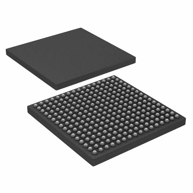


 工商网监
湘ICP备2023018690号
工商网监
湘ICP备2023018690号
