a
FEATURES RS-232 and RS-422 on One Chip Single +5 V Supply 0.1 F Capacitors Short Circuit Protection Excellent Noise Immunity Low Power BiCMOS Technology High Speed, Low Skew RS-422 Operation –40 C to +85 C Operations APPLICATIONS DTE-DCE Interface Packet Switching Local Area Networks Data Concentration Data Multiplexers Integrated Services Digital Network (ISDN) GENERAL DESCRIPTION
+5 V Powered RS-232/RS-422 Transceiver AD7306
FUNCTIONAL BLOCK DIAGRAM
V+ C1+ C1– R2 IN T1OUT T2OUT VCC R1 IN (B) R1 IN /R1 IN (A) T3OUT (B) T3OUT (A) NC 1 2 3 4 5 6 7 8 9 10 11 12 NC = NO CONNECT 24 23 22 21 20 V– C2– C2+ R2 OUT T1IN T2IN GND R1 OUT T3IN 232/422 SEL GND NC
AD7306 SOIC
TOP VIEW (Not to Scale)
19 18 17 16 15 14 13
The AD7306 line driver/receiver is a 5 V monolithic product which provides an interface between TTL signal levels and dual standard EIA RS-232/RS-422 signal levels. The part contains two RS-232 drivers, one RS-422 driver, one RS-232 receiver, and one receiver path which can be configured either as RS-232 or as RS-422. An internal charge pump voltage converter facilitates operation from a single +5 V power supply. The internal charge pump generates ± 10 V levels allowing RS-232 output levels to be developed without the need for external bipolar power supplies. A highly efficient charge pump design allows operation using non polarized, miniature 0.1 µF capacitors. This gives a considerable saving in printed circuit board space over conventional products which can use up to 10 µF capacitors. The charge pump output voltages may also be used to power external circuitry which requires dual supplies.
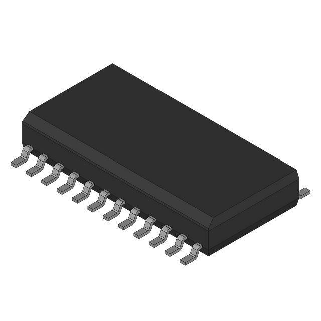
The RS-232 channels are suitable for communications rates up to 100 kHz and the RS-422 channels are suitable for high speed communications up to 5 MHz. The RS-422 transmitter complementary outputs are closely matched and feature low timing skew between the complementary outputs. This is often an essential requirement to meet tight system timing specifications. All inputs feature ESD protection, all driver outputs feature high source and sink current capability and are internally protected against short circuits on the outputs. An epitaxial layer is used to guard against latch-up. The part is available in a 24-lead SOIC and 24-pin plastic DIP package.
R EV. B
Information furnished by Analog Devices is believed to be accurate and reliable. However, no responsibility is assumed by Analog Devices for its use, nor for any infringements of patents or other rights of third parties which may result from its use. No license is granted by implication or otherwise under any patent or patent rights of Analog Devices.
One Technology Way, P.O. Box 9106, Norwood, MA 02062-9106, U.S.A. Tel: 617/329-4700 Fax: 617/326-8703
�AD7306–SPECIFICATIONS (V T
Parameter RS-232 DRIVER TTL Input Logic Low, VINL TTL Input Logic High, VINH Input Logic Current RS-232 High Level Output Voltage RS-232 Low Level Output Voltage Output Short Circuit Current Slew Rate Output Resistance (Powered Down) RS-232 RECEIVER Input Voltage Range RS-232 Input Threshold Low RS-232 Input Threshold High RS-232 Input Hysteresis RS-232 Input Resistance TTL Output Voltage Low, VOL TTL Output Voltage High, VOH RS-422 DRIVER TTL Input Logic Low, VINL TTL Input Logic High, VINH Logic Input Current Differential Output Voltage Common-Mode Output Voltage ∆|VOUT| for Complementary O/P States Output Short Circuit Current RS-422 RECEIVER Common-Mode Voltage Range Differential Input Threshold Voltage Input Voltage Hysteresis Input Resistance TTL Output Voltage Low, VOL TTL Output Voltage High, VOH 232/422 SEL Input Input Logic Low, VINL Input Logic High, VINH Logic Input Current POWER SUPPLY CURRENT ICC CHARGE PUMP VOLTAGE GENERATOR V+ Output Voltage V– Output Voltage Generator Rise Time
Specifications subject to change without notice.
CC
MAX
= +5 V 5%, C1 = C2 = C3 = C4 = 0.1 F. All specifications TMIN to unless otherwise noted.)
Typ Max 0.8 Units V V µA V V mA V/µs V/µs Ω V V V V kΩ V V V V µA V V V V mA V V mV kΩ V V V V µA mA V V µs Test Conditions/Comments
Min
2.0 5.0 –5.0 ±5 8 300 –15 0.8 0.1 3 3.5 0.1 7.3 –6.5 ± 12 20 4 10M
± 10
30
VIN = 0 V to VCC R L = 3 kΩ R L = 3 kΩ VOUT = 0 V, TA = 0°C to +70°C CL = 50 pF, RL = 3 kΩ CL = 2500 pF, RL = 3 kΩ VCC = 0 V, VOUT = ± 3 V
+15 1.3 1.7 0.4 5 0.2 4.8 2.4 1.0 7 0.4
IOUT = +4 mA IOUT = –4 mA
0.8 2.0 0.1 2 3 0.2 150 ±7 +0.2 70 5 0.2 4.8 7 0.4 ± 10 5.0
VIN = 0 V to VCC VCC = 5 V, RL Diff = ∞; Figure 3 RL Diff = 100 Ω; Figure 3 RL Diff = 100 Ω 0 V ≤ VCMR ≤ +7 V Typical RS-422 Input Voltage
很抱歉,暂时无法提供与“AD7306AR”相匹配的价格&库存,您可以联系我们找货
免费人工找货