-
-.. ANALOG
W DEVICES
CMOS10-Bit,
BufferedMultiplying
0/ A Converter
FEATURES
10-Bit Resolution
8-,9- & 10-Bit Linearity
Microprocessor Compatible
Double Buffered Inputs
Serial or Parallel Loading
DTL!TTL/CMOS Direct Interface
Nonlinearity Tempco: 2ppm of FSRfc
Gain Tempco: 10ppm of FSRfc
Very Low Power Dissipation
Very Low Feedthrough
OBS
OLE
GENERAL DESCRIPTION
FUNCTIONAL DIAGRAM
The AD7522 is a monolithic CMOS lO-bit multiplying D/A
converter, with an input buffer and a holding register, allowing
direct interface with microprocessors. Most applications require the addition of only an operational amplifier and a
reference voltage.
Vcc
DGND
The key to easy interface to a data bus is the AD7522's ability
to load the input buffer in two bytes (an 8-bit and a 2-bit byte),
and subsequently move this data to a holding register, where
the digital word is converted into an analog current or voltage
(with external operational amplifier). The input loading of
either 8 or 10 bits can be done in a parallel or serial mode.
Vou
TE
v." AGND
LDTR
RFB'
RFB2
Iou..
Iou"
The AD7522 is packaged in a 28-pin DIP, and operates with
a +15V main supply at 2mA max, and a logic supply of +5V
for TTL interface, or +10 to +15V for CMOS interface.
A thin film on high density CMOS process, using silicon
nitride passivation, ensures high reliability and excellent
stability.
ORDERING
Nonlinearity
DB' DBS
(MSB'
PIN CONFIGURATION
VDD
INFORMATION
0 to +70°C
2LSB (S-Bit)
AD7522JN
lLSB (9-Bit)
AD7522KN
1I2LSB (to-Bit) AD7522LN
DB1 DB6 DBS DB4 DB3 DB2 DB' DOO
(lOB'
Temperature Range
-25°C to +S5°C -55°C to +125°C
AD7522SD
AD7522JD
AD7522KD
AD7522TD
AD7522LD
AD7522UD
DGND
LDTR
Vcc
v."
SR'
RFB2
HBS
RFB'
LBS
IDtJT1
'DtJT2
AGND
SRD
(MSB) DM
PACKAGE IDENTIFICATION
DBS
DB1
Suffix "D": Ceramic DIP Package
Suffix UN": Plastic DIP Package
DB.
DBS
Information furnished by Analog Devices is believed to be accurate
and reliable. However, no responsibility is assumed by Analog Devices
for its use; nor for any infringements of patents or other rights of third
parties which may result from its use. No license is granted by implication or otherwise under any patent or patent rights of Analog Devices.
~~~-
-------
One Technology Way; Norwood, MA 02062-9106 U.S.A.
Tel: 617/329-4700
Twx: 710/394-6577
Telex: 174059
Cables: ANALOG NORWOODMASS
�SPECIFICATIONS
(Voo = +15V, Vcc = +5V, VREF = +10V,TA = +25°C unless otherwise noted)
TA
PARAMETER
STATIC ACCURACY
Resolution
Nonlinearity
OVER SPECIFIED
=+25°C
TEMP. RANGE
-
All
AD7522]
AD7522S
AD7522K
AD7522T
AD7522L
AD7522U
AD7522] ,K,L
Nonlinearity Tempco!
AD7522S,T,U
All
Gain Error
AD7522] ,K,L
Gain Error Tempco!
AD7522S,T,U
Output Leakage Current I All
at louTl or IOUT2
Power Supply Rejection AD7522],K,L
AC ACCURACY
All
Feedthrough Error!
Output Current
AD7522],K,L
Settling Time
10 Bits min
:t2LSB max
:t2LSB max
:tILSB max
:tILSB max
:t1/2LSB max
:tI/2LSB max
:tlppm FSR/C
High State Threshold
Input Current
LDAC Pulse Width!
HBS, LBS Pulse Width!
Serial Clock Frequency!
HBS, LBS Data Set Up2
Data Hold Time3
SC8 = "I"
10 Bits min
:t2LSB max
:tILSB max
:tI/2LSB max
typ
:to.3% Reading typ
:t5ppm of Reading/C
:t2ppm FSR/C max
:t2ppm FSR/C max
:t2.0% Reading max
:tIOppm of Reading/oC max
:tIOppm of ReadingtC max
2oonA max
typ
OBS
REFERENCE INPUT
Input Resistance
ANALOG OUTPUT
Output Capacitance
CoUTl
COUT2
COUTl
COUT2
DIGITAL INPUTS
Low State Threshold
IOUTl: DBO through DB9
IOUT2: DBO through DB9
IDD
ImV p-p typ, 10mV p-p max
500ns typ
5kU min/20kU max
AD7522],K,L
AD7522] ,K,L
AD7522] ,K,L
AD7522] ,K,L
120pF typ
40pF typ
4OpF typ
120pF typ
All
All
All
All
AD7522],K,L
All
All
All
All
All
0.8V max
1.5V max
2.4V min
13.5V min
I/lA typ
500ns min
500ns min
IMHz max
250ns min
All
All
2mA max
2mA max
(
5kU min/20kU max
TE
} All Data Input High
} All Data Inputs Low
500ns min, 200ns typ
0.8V max
1.5V max
2.4V min
13.5V min
Vee = +5V
Vee = +15V
Vee = +5V
Vee = +15V
5OOns min
5OOns min
IMHz max
250ns min
5OOnsmin
LDAC: 0 to +3V
HBS, LBS: 0 to +3V
} In Quiescent State
Notes
Specifications subject to change without notice.
I Guaranteed by design. Not tested.
. Data setup time is the minimum amount of time required for DBO DB9 to be stable prior to strobing HBS, LBS.
s Data hold time is the minimum amount of time required for DBO - DB9 to be stable after strobing HBS, LBS.
-
-2-
=1
VREF= 20V pop; 10kHz
To 0.05% of FSR for a FSR Step.
HBS and LBS Low to High
LDAC = 1
OLE
All
---
=0
5Oppm of Reading/% typ
POWER REQUIREMENTS
Ice
(
TEST CONDITIONS
--
-----
(
(
�(
ABSOLUTE MAXIMUM RATINGS
VREFtoGND
VDDtoGND
VcctoGND
VCCtoVDD"""""""""""""'"
Output Voltage (pins 6 & 7)
DAC CIRCUIT
GENERAL CIRCUIT INFORMATION
The AD7S22's DAC functional block consists of a highly
stable Silicon Chromium thin film R-2R ladder, and ten
SPOT N-channel current steering switches. Most applications require the addition of only an output operational
amplifier and a voltage or current reference.
:!:2SV
+17V
+17V
+0.4V
. . . . . . . . . . . . . -Q.3Vto
VDD
Operating Temperature
IN,KN,LNversions
Oto+70°C
"""""""""
The simplified 01 A circuit is shown in Figure 1. An inverted R-2R ladder structUre is used - that is, the binarily
weighted currents are switched between the louT1 and louT2
bus lines, thus maintaining a constant current in each ladder
leg independent of the switch state.
JD, KD,LDversions. . . . . . . . . . . . . . .-2SoC to +8SoC
SO,TD, UDversions. . . . . . . . . . . . . . -55°C to +12SoC
StorageTemperature. . . . . . . . . . . . . . . . -65°C to +lS0oC
Power Dissipation (Package)
Up to +SOoC:
Plastic(SuffixN)
.1200mW
Ceramic (Suffix D) . . . . . . . . . . . . . . . . . . .1000mW
Derate Above +SOOCby
Plastic(SuffixN)
.12mWtC
Ceramic (Suffix D) . . . . . . . . . . . . . . . . . . 10mWtC
Digital Input Voltage Range. . . . . . . . . . . . . .VDDto GND
R
OBS
(
CAUTION:
(
DESCRIPTION
R
R
2R
VREF
LDTR
2R
2R
2R
2R
5-2
IoUT2
OLE
6
6
MSB
1. Do not apply voltages higher than Vcc to SRO.
2. Do not apply voltages higher than VDD or less than GND to
any other inputloutput terminal except VREF' RFB1 or
RFBZ'
3. The digital control inputs are zener protected, however
permanent damage may occur on unconnected units
under high energy electrostatic fields. Keep unused units
in conductive foam at all times.
'OUT!
6
6
LSB
R
2"
R
2"
RFBI
RFB2
TE
Figure 1. DAC Functional Diagram
EQUIVALENT CIRCUIT
The DAC equivalent circuit is shown in Figure 2. The curren
source ILEAKAGEis composed of surface and junction leakages to the substrate, while the IREF/1024 current source
represents the 1LSB of current lost through the ladder termi
nation resistor to ground. The CuUTl and CuUTZ output
capacitances are as shown when the DAC latches feed the
DAC with all "1 's." If the DAC latches are loaded with all
4. VCCshould never exceed VDD by more than OAV,
especially during power ON or OFF sequencing.
TERMINOLOGY
"O's," CuUTl is 37pF, while CoUT2 is 120pF. In addition,
CSD is replaced by 10 ohms, and the 10 ohm RON in IOUTl
is replaced by a CSD of 10pF. When fast amplifiers are used,
it will be necessary to provide phase compensation (in the
form of feedback capacitance) to cancel the pole formed by
RFEEDBACKand CuUT if stability is to be maintained.
RESOLUTION
Value of the LSB. For example, a unipolar n-bit converter
has a resolution of (2-n) (VREF)' A bipolar n-bit converter
has a resolution of [2-(n-1)] [VREF]' Resolution in no way
im plies lineari ty .
CpARASITIC
~0.2pF
GAIN
RFEEOBACK
10K
r R~A~O;R
- - - --jI-- - - - - - - - - -
The "gain" of a converter is that analog scale factor setting
that establishes the nominal conversion relationship, e.g.,
10V full scale. It is a linear error which can be externally
adjusted (see gain adjusrment on next page).
I
VREF- ~'
INPUT
NOMINAL
10K
NOMINAL
loUT!
I
I~I
I
1024
,
I
I
I
I
OUTPUT LEAKAGE CURRENT
Current which appears on the OUT1 terminal when the DAC
register is loaded with all "O's" or on the OUT2 terminal
when the DAC register is loaded with all "1 's."
'OUT2
I
I
COD
10pF
L--H
J
CpARAsmc
~0.2pF
Figure 2. Equivalent Circuit (Shown for all Digital
Inputs High)
-
-
-
-3-
--
--
�PIN FUNCTION DESCRIPTION
PIN
1
MNEMONIC
DESCRIPTION
VDD
LDTR
+15V (nominal) Main Supply.
Reference
4
VREF
RFB2
RFEEDBACK 7 2; gives full scale equal to VREF/2.
5
RFBI
RFEEDBACK' used for normal unity gain (at full scale) D/A conversion.
6
IoUTl
DAC Current OUTI Bus. Normally terminated
7
DAC Current OUT2 Bus, terminated
8
IoUTZ
AGND
Analog Ground.
9
SRO
Serial Output.
2
3
R-2R Ladder Termination
10
DB8
Data Bit 8.
12
DB7
Data Bit 7.
13
DB6
089T
DB5
15
or terminated
at 'oUT2 for bipolar operation.
at virtUal ground of output amplifier.
at ground for unipolar operation, or virtual ground of op amp for bipolar operation.
Back gate of DAC N-channel SPOT current steering switches.
An auxiliary output
for recovering data in the input buffer.
Data Bit 9. Most significant parallel data input.
11
14
Resistor. Normally grounded for unipolar operation
Voltage Input. Since the AD7522 is a multiplying DAC, VREF may vary over the range of :!:10V.
Data Bit 6.
Data
Note 1
Data
Data
Data
Data
Bit
Bit
Bit
Bit
Bit
5.
4.
3.
2.
1.
OBS
16
DB3
17
DB2
18
DBI
19
DMl
DBO
20
SC8
Data Bit O. Least significant parallel data input.
8-Bit Short Cycle Control. When in serial mode, if scs is held to Logic "0", the two least significant input latches in the input buffer
are bypassed to provide proper serial loading of 8-bit serial words. If SC8 is held to Logic "1", the AD7522 will accept a to-bit serial
OLE
word.
-
Data bits 0 (LSB) and DBI are in a parallel load mode when SC8
from being loaded.
=0
and should be tied to a logic low state to prevent fal~ data
21
SPC
SeriallParalleI Control. If SPC is a Logic "0", the AD7522 will load parallel data appearing on DBO through DB9 into the input buffer
when the appropriate strobe inputs are exercised (see HBS and LBS).
If SPC is a Logic "1", the AD7522 will load serial data appearing on Pin 26 into the input buffers. Each serial data bit must be
"suobed" into the buffer with the HBS and LBS.
22
LDAC
23
NC
Load DAC: When LDAC is a Logic "0", the AD7522 is in the "hold" mode, and digital activity in the input buffer is locked out.
When LDAC is a Logic "I ", the AD7522 is in the "load" mode, and data in the input buffer loads the DAC register.
No Connection.
24
LBS
Low Byte Strobe. When in "parallel load" mode (SPC = 0), parallel data appearing on the DBO (LSB) through DB7 inputs will be
"clocked" into the input buffer on the positive going edge of the LBS.
When in "serial load" mode (SPC = 1), serial data bits appearing at the serial input terminal, Pin 26, will be "clocked" into the input
buffer on the positive going edge of HBS and LBS. (HBS and LBS must be clocked simultaneously when in "serial load" mode.)
25
HBS
High Byte Strobe. When in "parallel load" mode (SPC = 0), parallel data appearing on the DB9 (MSB) and DB8 data inputs will be
"clocked" into the input buffer on the positive going edge of HBS.
TE
When in "serial load" mode (SPC = I), serial data bits appearing at the serial input terminal, Pin 26, will be "clocked" into the input
buffer on the positive going edges of HBS and LBS. (HBS and LBS muSt be clocked simultaneously when in "serial load" mode.)
26
SRI
Serial Input.
27
VCC
Logic Supply. If +5V is applied, all digital inputs/outputs
are CMOS compatible.
28
DGND
Note I, Logie "I"
are TTL compatible.
If +10V to +15V is applied, digital inputs/outputs
Digital Ground
applied to a data bit steers that bit's cun-ent to the 10UTI
APPLICATIONS
(Note:
tenninaJ.
Protection Schottky CR3 in Figure 3 and Figure 4 is not required when using TRI-FET
amps such as the AD542 or AD544).
VDD
+15V
UNIPOLAR OPERATION
Figure 3 shows the analog circuit connections required for
unipolar operation. The input code/output voltage relationship is shown in Table I.
Zero Offset Adjustment
1. Adjust the op amp's offset potentiometer
the amplifier junction.
Vcc
+5V TO +15V
CAI
AI
GAIN ADJ
5OOQ
27
4-
AF82
A2 GAIN
500Q
VREF
>IOY
for < 1mV on
ADJ
5,AF81
AD7522
DAC
Gain Adjustment
1. Set Rl and R2 to oQ. Load the DAC register with all
"l's."
'OUT
1
CA3
lOUT
2
2, If analog out is greater than -VREF' increase Rl for required full scale output, If analog out is less than -VREF'
increase R2 for required full scale output.
LOTA
Figure 3. Unipolar Binary Operation
(2-Quadrant Multiplication)
-4-
ANALOG
OUTPUT
�r
f/i/-- ,;~.;:,
~'..-
DIGITAL INPUT
ANALOG
1111111111
-VREF
(1 -
2010)
1000000001
-VREF
(1/2
+ 2-10)
-
Voo
+15V
OUTPUT
1000000000
-VREF/2
0111111111
-VREF
(1/2
0000000001
-VREF
(2010)
0000000000
Vcc
+5V TO +15V
2010)
AD7522
DIA
CONVERTER
0
Table I. Unipolar Code Table
26~
211 .SPC
BIPOLAR OPERATION
Figure 4:shows the analog circuit connections required for
bipolar operation. The input code/ouput voltage relationship
is shown in Table II.
"
Vcc
+5VTO +15V
CR2
Figure 5. Single Byte Parallel Loading
n
When data is stable on the parallel inputs (DBO-DB9), it can be
transferred into the input buffer on the positive edge of the
strobe pulse.
R3
2Ok!1
27
5
VREF
t10V
I
RfBI
R2
soon
6 ,'oun
AD7522
DAC
7 .'Dun
2' LDTR
Figure 4. Bipolar Operation
~
STROBE
LOAD(1)/
HOLD(01
OBS
Voo
+15V
20'_~
R5
2Ok!1
OLE
Data is transferred from the input buffer to the DAC register
when LDAC is a Logic "1." LDAC is a level-actuated (versus
edge-triggered) function and must be held "high" at least
O.5l1sfor data transfer to occur.
MSB
With the DAC register loaded to 10 0000 0000 adjust
Rl so that ANALOG
OUTPUT
= OVo
OUTPUT
= OV.
Full-scale
Voo
+15V
Vee
+5V TO +15V
10
Alternatively,
§
Rl, R2 may be omitted and the ratios of R3, R4
varied for ANALOG
TE
TWO BYTE PARALLEL LOADING
Figures 6 and 7 show the logic connections and timing requirements for interfacing the AD75 22 to an 8-bit data bus for two
byte loading of a lO-bit word.
I
e'"
trimming
can be accomplished by adjusting the amplitude of
VREF or by varying the value of R5.
If Rl, R2 are not used, then resistors R3, R4 and R5
should be ratio matched to 0.05% to ensure gain error
performance to the data sheet specification. When
operating over a wide temperature range, it is important
that the resistors be of the same type so that their temperature coefficients match.
"'
..I..
DO
D7
DB8
DB7
D6
DB6
D5
DB5
D4
DB4
11
12
13
14
15
AD7522
DIA
CONVERTER
D
DB3
c
D2
DB2
iii
..
17
26
DI
DBI
18
21
DO
D80
LSB
19
20
I-
16
SPC
.
seD
LBS
HBS
LDAC
DIGITAL INPUT
ANALOG OUTPUT
1111111111
+VREF
1000000001
+VREF (Z-9)
0
1000000000
(1
Figure 60 Two Byte Parallel Loading
- 2-9)
0111111111
-VREF (2-9)
0000000001
-VREF (1 - 2-9)
0000000000
-VREF
DATA
BUS
LBS
HBS
Table 1/. Bipolar Code Table
SINGLE BYTE PARALLEL LOADING
Figure 5 illustrates the logic connections for loading single byte
parallel data into the input buffer. DBO should be grounded on
"K" and "T" versions, and DBO and DBI should be grounded
on ")" and "S" versions for monotonic operation of the DAC.
DB9 is always the MSB, whether 8-bit, 9-bit, or lO-bit linear
AD7522's are used.
LDAC
MOST SIGNIFICANT
DATA BYTE
LEAST SIGNIfICANT
DATA BYTE
LOAD LEAST SIGNifiCANT
BYTE INTO INPUT REGISTER
LOAO MOST SIGNifiCANT..
BYTE INTO INPUT REGISTER
UPDATE
DAC---rI
OUTPUT
=:::J
L
Figure 7. Timing Diagram
First, the least significant data byte (DBO through DB7) is
loaded into the input buffer on the positive edge of LBS. Subsequently, the data bus is used for status indication and
-5-
�2. Diode CR3 on Figure 3 and Figure 4 clamps the amplifier junction to -300mV if it attempts to swing negative
during power up or power down. The input structures
of some high-speed op amps can supply substantial
current under the transient conditions encountered during power sequencing. It is recommended that the PC
layout be able to accommodate the diodes.
instruction fetching by the CPO. When the most significant
data byte (DB8 and DB9) is available on the bus, the input
buffer is loaded on the positive edge of HBS. The DAC register
updates to the new 10-bit word when LDAC is "high." LDAC
may be exercised coincident with, or at any time after HBS
loads the second byte of data into the input buffer.
SERIAL LOADING
Figure 8 and Figure 9 show the connections and timing
diagram for serial loading.
To load a lO-bit word (SC8 = 1), HBS and LBS must be strobed
simultaneously with exactly 10 positive edges to clock the
serial data into the input buffer. For 8-bit words (SC8 = 0), only
8 positive edges are required.
Vcc
+5VTO +15V
3. Fast op amps will require phase compensation for stability
due to the pole formed by COUT1 or COUT2 and
RFEEDBACK.
LOAD
SRI
VDD
+15V
DAC
SERIAL
DATA OUT
AD7522
DAC
SERIAL DATA
(IO.BIT
MODEl
CLOCK
(8-8IT
IN
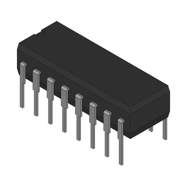
28 PIN CERAMIC DIP (SUFFIX D)
:
~
7
OLE
-.1f-
28-PIN PLASTIC DIP (SUFFIX N)
8
MODE)
LOAD
IS-BIT
IN
MODE)
DAC
DAC
MODEl
Ii
C'
C
LOGIC "0" FOR 8.81T MOOE
LOGIC "I" FOR '0.8IT MODE
SR'
LOAD
It
21
Figure 8. Serial 8- and to-Bit Loading
(Analog Outputs Not Shown for Clarity)
CLOCK
Ii
I
SPC
~
20f---
(lD-BIT
Ii
OUTLINE DIMENSIONS
Dimensionsshown in inches and (nun).
0' SRO
26
w
f'
4. During serial loading, all data inputs (DBO through BD9),
should be grounded.
OBS
SERIAL DATA
IN
CLOCK IN
(
UPDATE
TlME::::::fl
L
Figure 9. Timing Diagram for Serial 8- and to-Bit Loading
[~~:::::::~]1:
...~
I
0.14..68'
1.45136.831
1.44136.58)
..1
15.081
MAX
APPLICATION HINTS
'-~II~
~~
0'2~
1. CR1 and CR2 on Figures 3 and 4 protect the AD7522
against latch-up Vcc exceeds VDD' and may be omitted
if VDD and Vcc are driven from the same voltage.
TE
~~~~
0.045
".151
-H-0.015 10.3811
-1
~
0.095
12.421
f-~~
Ir 0.5"
"5.091
~
0.01210.3051 :--T
~017514451
~
(
~
LEAD NO. IIDE""FlEO
8Y DOT OR NOTCH
LEAOS ARE SOLDER OR TIN PLATED KOVAR OR ALLOY 42
(
L
~
;;
-6-
-
---
~
--
-
-
--
�