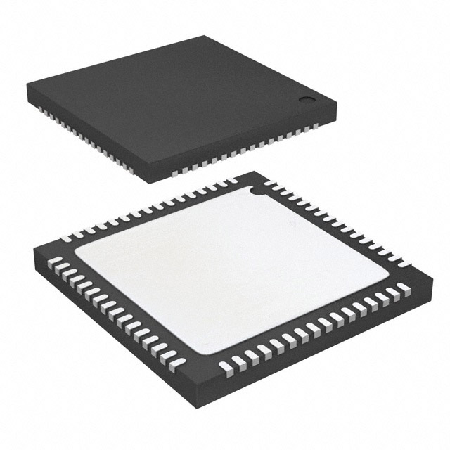
8-Channel, 24-Bit,
Simultaneous Sampling ADC
AD7771
Data Sheet
FEATURES
8-channel, 24-bit simultaneous sampling ADC
Single-ended or true differential inputs
PGA per channel (gains of 1, 2, 4, and 8)
Low dc input current
±4 nA (differential)/±8 nA (single-ended)
Up to 128 kSPS ODR per channel
Programmable ODRs and bandwidth
SRC for coherent sampling
Sampling rate resolution up to 15.2 × 10⁻⁶ SPS
Low latency sinc3 and sinc5 filter paths
Adjustable phase synchronization
Internal 2.5 V reference
Two power modes
High resolution mode
Low power mode
Optimizes power dissipation and performance
Low resolution SAR ADC for system and chip diagnostics
Power supply
Bipolar (±1.65 V) or unipolar (3.3 V) supplies
Digital I/O supply: 1.8 V to 3.6 V
Performance temperature range: −40°C to +105°C
Functional temperature range: −40°C to +125°C
Performance
Combined ac and dc performance
107 dB SNR/dynamic range at 32 kSPS in high resolution
mode (sinc5)
−109 dB THD
±8 ppm of FSR INL
±15 µV offset error
±0.1% FS gain error
±10 ppm/°C typical temperature coefficient
APPLICATIONS
Power quality and measurement applications
General-purpose data acquisition
Electroencephalography (EEG)
Industrial process control
voltage from 1 V up to 3.6 V. The analog inputs accept unipolar
(0 V to VREF) or true bipolar (±VREF/2 V) analog input signals with
3.3 V or ±1.65 V analog supply voltages, respectively. The analog
inputs can be configured to accept true differential or single-ended
signals to match different sensor output configurations.
Each channel contains an ADC modulator and a sinc3/sinc5, low
latency digital filter. A sample rate converter (SRC) is provided to
allow fine resolution control over the AD7771 output data rate
(ODR). This control can be used in applications where the ODR
resolution is required to maintain coherency with 0.01 Hz
changes in the line frequency. The SRC is programmable through
the serial port interface (SPI). The AD7771 implements two
different interfaces: a data output interface and SPI control
interface. The ADC data output interface is dedicated to transmitting the ADC conversion results from the AD7771 to the
processor. The SPI writes to and reads from the AD7771
configuration registers and for the control and reading of data
from the successive approximation register (SAR) ADC. The SPI
can also be configured to output the Σ-Δ conversion data.
The AD7771 includes a 12-bit SAR ADC. This ADC can be used
for AD7771 diagnostics without having to decommission one of
the Σ-Δ ADC channels dedicated to system measurement functions. With the use of an external multiplexer, which can be
controlled through the three general-purpose input/output pins
(GPIOs), and signal conditioning, the SAR ADC can validate
the Σ-Δ ADC measurements in applications where functional
safety is required. In addition, the AD7771 SAR ADC includes
an internal multiplexer to sense internal nodes.
The AD7771 contains a 2.5 V reference and reference buffer. The
reference has a typical temperature coefficient of ±10 ppm/°C.
The AD7771 offers two modes of operation: high resolution
mode and low power mode. High resolution mode provides a
higher dynamic range while consuming 16.6 mW per channel;
low power mode consumes only 5.25 mW per channel at a
reduced dynamic range specification.
GENERAL DESCRIPTION
The specified operating temperature range is −40°C to +105°C,
although the device is operational up to +125°C.
The AD77711 is an 8-channel, simultaneous sampling analog-todigital converter (ADC). Eight full Σ-Δ ADCs are on-chip. The
AD7771 provides an ultralow input current to allow direct sensor
connection. Each input channel has a programmable gain stage
allowing gains of 1, 2, 4, and 8 to map lower amplitude sensor
outputs into the full-scale ADC input range, maximizing the
dynamic range of the signal chain. The AD7771 accepts a VREF
Note that throughout this data sheet, certain terms are used to
refer to either the multifunction pins or a range of pins. The
multifunction pins, such as DCLK0/SDO, are referred to either
by the entire pin name or by a single function of the pin, for
example, DCLK0, when only that function is relevant. In the
case of ranges of pins, AVSSx refers to the following pins:
AVSS1A, AVSS1B, AVSS2A, AVSS2B, AVSS3, and AVSS4.
1
This product is protected by at least U.S. Patent No. 9,432,043.
Rev. A
Document Feedback
Information furnished by Analog Devices is believed to be accurate and reliable. However, no
responsibility is assumed by Analog Devices for its use, nor for any infringements of patents or other
rights of third parties that may result from its use. Specifications subject to change without notice. No
license is granted by implication or otherwise under any patent or patent rights of Analog Devices.
Trademarks and registered trademarks are the property of their respective owners.
One Technology Way, P.O. Box 9106, Norwood, MA 02062-9106, U.S.A.
Tel: 781.329.4700 ©2017–2018 Analog Devices, Inc. All rights reserved.
Technical Support
www.analog.com
�AD7771
Data Sheet
TABLE OF CONTENTS
Features .............................................................................................. 1
Σ-∆ Output Data............................................................................. 54
Applications ....................................................................................... 1
ADC Conversion Output—Header and Data ........................ 54
General Description ......................................................................... 1
Sample Rate Converter (SRC) (SPI Control Mode) .............. 55
Revision History ............................................................................... 3
Data Output Interface ................................................................ 57
Functional Block Diagram .............................................................. 4
Calculating the CRC Checksum .............................................. 61
Specifications..................................................................................... 5
Register Summary .......................................................................... 62
DOUTx Timing Characterististics ............................................. 9
Register Details ............................................................................... 66
SPI Timing Characterististics ................................................... 10
Channel 0 Configuration Register ........................................... 66
Synchronization Pins and Reset Timing Characteristics ...... 11
Channel 1 Configuration Register ........................................... 66
SAR ADC Timing Characterististics ....................................... 12
Channel 2 Configuration Register ........................................... 67
GPIO SRC Update Timing Characterististics......................... 12
Channel 3 Configuration Register ........................................... 67
Absolute Maximum Ratings .......................................................... 13
Channel 4 Configuration Register ........................................... 68
Thermal Resistance .................................................................... 13
Channel 5 Configuration Register ........................................... 68
ESD Caution ................................................................................ 13
Channel 6 Configuration Register ........................................... 69
Pin Configuration and Function Descriptions ........................... 14
Channel 7 Configuration Register ........................................... 69
Typical Performance Characteristics ........................................... 17
Disable Clocks to ADC Channel Register .............................. 70
Terminology .................................................................................... 32
Channel 0 Sync Offset Register ................................................ 70
Theory of Operation ...................................................................... 34
Channel 1 Sync Offset Register ................................................ 70
Analog Inputs .............................................................................. 34
Channel 2 Sync Offset Register ................................................ 70
Transfer Function ....................................................................... 35
Channel 3 Sync Offset Register ................................................ 71
Core Signal Chain....................................................................... 36
Channel 4 Sync Offset Register ................................................ 71
Capacitive PGA ........................................................................... 36
Channel 5 Sync Offset Register ................................................ 71
Internal Reference and Reference Buffers ............................... 36
Channel 6 Sync Offset Register ................................................ 71
Integrated LDOs ......................................................................... 37
Channel 7 Sync Offset Register ................................................ 71
Clocking and Sampling .............................................................. 37
General User Configuration 1 Register ................................... 72
Digital Reset and Synchronization Pins .................................. 37
General User Configuration 2 Register ................................... 73
Digital Filtering ........................................................................... 38
General User Configuration 3 Register ................................... 74
Shutdown Mode.......................................................................... 38
Data Output Format Register ................................................... 74
Controlling the AD7771 ............................................................ 39
Main ADC Meter and Reference Mux Control Register ...... 75
Pin Control Mode....................................................................... 39
Global Diagnostics Mux Register ............................................. 76
SPI Control .................................................................................. 42
GPIO Configuration Register ................................................... 76
Digital SPI .................................................................................... 45
GPIO Data Register.................................................................... 77
RMS Noise and Resolution............................................................ 48
Buffer Configuration 1 Register ............................................... 77
High Resolution Mode............................................................... 48
Buffer Configuration 2 Register ............................................... 77
Low Power Mode ........................................................................ 49
Channel 0 Offset Upper Byte Register..................................... 78
Diagnostics and Monitoring ......................................................... 50
Channel 0 Offset Middle Byte Register ................................... 78
Self Diagnostics Error ................................................................ 50
Channel 0 Offset Lower Byte Register..................................... 78
Monitoring Using the AD7771 SAR ADC (SPI Control
Mode) ........................................................................................... 51
Channel 0 Gain Upper Byte Register....................................... 78
Σ-Δ ADC Diagnostics (SPI Control Mode) ............................ 53
Channel 0 Gain Middle Byte Register ..................................... 78
Channel 0 Gain Lower Byte Register ....................................... 79
Rev. A | Page 2 of 99
�Data Sheet
AD7771
Channel 1 Offset Upper Byte Register .....................................79
Channel 6 Gain Lower Byte Register ....................................... 86
Channel 1 Offset Middle Byte Register ....................................79
Channel 7 Offset Upper Byte Register ..................................... 86
Channel 1 Offset Lower Byte Register .....................................79
Channel 7 Offset Middle Byte Register.................................... 86
Channel 1 Gain Upper Byte Register........................................79
Channel 7 Offset Lower Byte Register ..................................... 86
Channel 1 Gain Middle Byte Register ......................................80
Channel 7 Gain Upper Byte Register ....................................... 87
Channel 1 Gain Lower Byte Register........................................80
Channel 7 Gain Middle Byte Register ...................................... 87
Channel 2 Offset Upper Byte Register .....................................80
Channel 7 Gain Lower Byte Register ....................................... 87
Channel 2 Offset Middle Byte Register ....................................80
Channel 0 Status Register .......................................................... 87
Channel 2 Offset Lower Byte Register .....................................80
Channel 1 Status Register .......................................................... 88
Channel 2 Gain Upper Byte Register........................................81
Channel 2 Status Register .......................................................... 88
Channel 2 Gain Middle Byte Register ......................................81
Channel 3 Status Register .......................................................... 89
Channel 2 Gain Lower Byte Register........................................81
Channel 4 Status Register .......................................................... 89
Channel 3 Offset Upper Byte Register .....................................81
Channel 5 Status Register .......................................................... 90
Channel 3 Offset Middle Byte Register ....................................81
Channel 6 Status Register .......................................................... 90
Channel 3 Offset Lower Byte Register .....................................82
Channel 7 Status Register .......................................................... 91
Channel 3 Gain Upper Byte Register........................................82
Channel 0/Channel 1 DSP Errors Register.............................. 91
Channel 3 Gain Middle Byte Register ......................................82
Channel 2/Channel 3 DSP Errors Register.............................. 92
Channel 3 Gain Lower Byte Register........................................82
Channel 4/Channel 5 DSP Errors Register.............................. 92
Channel 4 Offset Upper Byte Register .....................................82
Channel 6/Channel 7 DSP Errors Register.............................. 93
Channel 4 Offset Middle Byte Register ....................................83
Channel 0 to Channel 7 Error Register Enable Register ....... 93
Channel 4 Offset Lower Byte Register .....................................83
General Errors Register 1 ........................................................... 94
Channel 4 Gain Upper Byte Register........................................83
General Errors Register 1 Enable .............................................. 94
Channel 4 Gain Middle Byte Register ......................................83
General Errors Register 2 ........................................................... 95
Channel 4 Gain Lower Byte Register........................................83
General Errors Register 2 Enable .............................................. 95
Channel 5 Offset Upper Byte Register .....................................84
Error Status Register 1 ................................................................ 96
Channel 5 Offset Middle Byte Register ....................................84
Error Status Register 2 ................................................................ 96
Channel 5 Offset Lower Byte Register .....................................84
Error Status Register 3 ................................................................ 97
Channel 5 Gain Upper Byte Register........................................84
Decimation Rate (N) MSB Register ......................................... 97
Channel 5 Gain Middle Byte Register ......................................84
Decimation Rate (N) LSB Register ........................................... 97
Channel 5 Gain Lower Byte Register........................................85
Decimation Rate (IF) MSB Register ......................................... 97
Channel 6 Offset Upper Byte Register .....................................85
Decimation Rate (IF) LSB Register .......................................... 98
Channel 6 Offset Middle Byte Register ....................................85
SRC Load Source and Load Update Register .......................... 98
Channel 6 Offset Lower Byte Register .....................................85
Outline Dimensions ........................................................................ 99
Channel 6 Gain Upper Byte Register........................................85
Ordering Guide ........................................................................... 99
Channel 6 Gain Middle Byte Register ......................................86
REVISION HISTORY
6/2018—Rev. 0 to Rev. A
Changes to IAVDD2x Parameter, Table 1 ............................................. 8
Changes to AUXAIN± Parameter, Table 7 ..................................13
Changes to Table 13 ........................................................................39
Changes to Phase Adjustment Section .........................................42
Added Table 17; Renumbered Sequentially .................................43
Added Figure 121; Renumbered Sequentially ............................. 47
Changes to Figure 132 Caption and Figure 133 Caption........... 57
Updated Outline Dimensions........................................................ 99
Changes to Ordering Guide ........................................................... 99
6/2017—Revision 0: Initial Version
Rev. A | Page 3 of 99
�AD7771
Data Sheet
FUNCTIONAL BLOCK DIAGRAM
AVDD1x
REFx+ REFx–
AVDD2x AREGxCAP
COMMONMODE
VOLTAGE
ANALOG
LDO
IOVDD
DREGCAP
DIGITAL
LDO
2.5V REF
AIN0+
AIN0–
AIN1+
AIN1–
AIN2+
AIN2–
AIN3+
AIN3–
AIN4+
AIN4–
AIN5+
AIN5–
AIN6+
AIN6–
AIN7+
AIN7–
280mV p-p
EXT_REF
INT_REF
GAIN
OFFSET
Σ-Δ ADC
SINC3/
SINC5
SRC
FILTER
GAIN
OFFSET
PGA
Σ-Δ ADC
SINC3/
SINC5
SRC
FILTER
GAIN
OFFSET
PGA
Σ-Δ ADC
SINC3/
SINC5
SRC
FILTER
GAIN
OFFSET
PGA
Σ-Δ ADC
SINC3/
SINC5
SRC
FILTER
GAIN
OFFSET
PGA
Σ-Δ ADC
SINC3/
SINC5
SRC
FILTER
GAIN
OFFSET
GAIN
OFFSET
GAIN
OFFSET
Σ-Δ ADC
PGA
REFERENCES
REFERENCES
REFERENCES
REFERENCES
REFERENCES
PGA
Σ-Δ ADC
SINC3/
SINC5
SRC
FILTER
PGA
Σ-Δ ADC
SINC3/
SINC5
SRC
FILTER
REFERENCES
REFERENCES
XTAL2/MCLK
SYNC_IN
SYNC_OUT
START
SINC3/
SINC5
SRC
FILTER
PGA
XTAL1
CLOCK
MANAGER
DCLK
DRDY
DATA OUTPUT
INTERFACE
DOUT2
DOUT1
DOUT0
REGISTER MAP
AND
LOGIC CONTROL
RESET
FORMAT1
FORMAT0
HARDWARE
MODE
CONFIGURATION
MODE3/ALERT
MODE2/GPIO2
MODE1/GPIO1
MODE0/GPIO0
ALERT/CS
SPI INTERFACE
AUXAIN+
AUXAIN–
DOUT3
DCLK2/SCLK
DCLK1/SDI
DCLK0/SDO
AD7771
SAR ADC
DIAGNOSTIC
INPUTS
AVSSx
AVDD4
CONVST_SAR
Figure 1.
Rev. A | Page 4 of 99
13802-001
VCM
REF_OUT
�Data Sheet
AD7771
SPECIFICATIONS
AVDD1x = 1.65 V, AVSSx 1 = −1.65 V (dual supply operation), AVDD1x = 3.3 V, AVSSx = analog ground (AGND) (single-supply operation),
AVDD2x − AVSSx = 2.2 V to 3.6 V; IOVDD = 1.8 V to 3.6 V; DGND = 0 V, REFx+/REFx− = 2.5 V AVSSx (internal/external), master clock
(MCLK) = 8192 kHz for high resolution mode and 4096 kHz for low power mode, ODR = 128 kSPS for high resolution mode and 32 kSPS
for low power mode; all specifications at TMIN to TMAX, unless otherwise noted.
Table 1.
Parameter
ANALOG INPUTS
Differential Input Voltage Range
Single-Ended Input Voltage Range
AINx± Common-Mode Input Range
Absolute AINx± Voltage Limits
DC Input Current
Differential
Single-Ended
Input Current Drift
AC Input Capacitance
PROGRAMMABLE GAIN AMPLIFIER (PGA)
Gain Settings (PGAGAIN)
Bandwidth
Small Signal
Large Signal
REFERENCE
Internal
Initial Accuracy
Temperature Coefficient
Reference Load Current, IL
DC Power Supply Rejection
Load Regulation, ∆VOUT/∆IL
Voltage Noise, eN p-p
Voltage Noise Density, eN
Turn On Settling Time
External
Input Voltage
Buffer Headroom
REFx− Input Voltage
Average REFx± Input Current
Test Conditions/Comments
Min
Typ
VREF = (REFx+ − REFx−)
AVSSx + 0.10
(AVDD1x +
AVSSx)/2
AVSSx + 0.10
High resolution mode
Low power mode
High resolution mode
Low power mode
Max
Unit
±VREF/PGAGAIN
0 to VREF/PGAGAIN
AVDD1x − 0.10
V
V
V
AVDD1x − 0.10
V
±4
±1
±8
±2
50
8
nA
nA
nA
nA
pA/°C
pF
1, 2, 4, or 8
High resolution mode
Low power mode
High resolution mode
Low power mode
REF_OUT, TA = 25°C
2
512
See Figure 39, Figure 40, and Figure 44
See Figure 42, Figure 43, and Figure 47
2.495
2.5
±10
−10
Line regulation
VREF = (REFx+ − REFx−)
2.505
±38
+10
V
ppm/°C
mA
dB
µV/mA
µV rms
nV/√Hz
ms
AVDD1x
AVDD1x − 0.1
AVDD1x − REFx+
V
V
V
95
100
6.8
273.5
1.5
0.1 Hz to 10 Hz
1 kHz, 2.5 V reference
100 nF
1
AVSSx + 0.1
2.5
AVSSx
Current per channel
Reference buffer disabled,
high resolution mode
Reference buffer precharge mode
(pre-Q), high resolution mode
Reference buffer disabled,
low power mode
Reference buffer pre-Q,
low power mode
Reference buffer enabled,
high resolution mode
Reference buffer enabled,
low power mode
Rev. A | Page 5 of 99
MHz
kHz
18
µA/V
600
nA/V
4.5
µA/V
100
nA/V
12
nA/V
5
nA/V
�AD7771
Parameter
TEMPERATURE RANGE
Specified Performance
Functional 2
TEMPERATURE SENSOR
Accuracy
DIGITAL FILTER RESPONSE
Group Delay
Settling Time
Pass Band
Decimation Rate
Sinc3
Sinc5
CLOCK SOURCE
Frequency
Duty Cycle
Σ-Δ ADC
Speed and Performance
Resolution
ODR
No Missing Codes
AC Accuracy
Dynamic Range
128 kSPS
32 kSPS
16 kSPS
4 kSPS
32 kSPS
8 kSPS
8 kSPS
2 kSPS
Total Harmonic Distortion (THD)
Signal-to-Noise-and-Distortion Ratio
(SINAD)
Spurious-Free Dynamic Range
(SFDR)
Intermodulation Distortion (IMD)
DC Power Supply Rejection
DC Common-Mode Rejection Ratio
Crosstalk
DC ACCURACY
Integral Nonlinearity (INL)
High Resolution
Data Sheet
Test Conditions/Comments
Min
TMIN to TMAX
TMIN to TMAX
−40
−40
Typ
Max
Unit
+105
+125
°C
°C
±2
°C
See the SRC Group Delay section
See the Settling Time section
See the SRC Bandwidth section
See the SRC Bandwidth section
−0.1 dB
−3 dB
High resolution mode
Low power mode
16
16
4095.99
2048
0.655
1.3
45:55
8.192
4.096
55:45
50:50
24
High resolution mode
Low power mode
Sinc3, up to 24 kSPS
Sinc5
128
32
24
24
Shorted inputs, PGAGAIN = 1
High resolution mode (sinc5)
High resolution mode (sinc5)
High resolution mode (sinc3)
High resolution mode (sinc3)
Low power mode (sinc5)
Low power mode (sinc5)
Low power mode (sinc3)
Low power mode (sinc3)
−0.5 dBFS, high resolution mode
−0.5 dBFS, low power mode
fIN = 60 Hz
High resolution mode, 16 kSPS,
PGAGAIN = 1
fA = 50 Hz, fB = 51 Hz,
high resolution mode
fA = 50 Hz, fB = 51 Hz,
low power mode
AVDD1x = 3.3 V
Bits
kSPS
kSPS
Bits
Bits
95
107
105.9
116
94.5
106.5
95.8
111.8
−109
−105
106
dB
dB
dB
dB
dB
dB
dB
dB
dB
dB
dB
132
dB
−125
dB
−105
dB
−90
dB
dB
dB
80
−120
Endpoint method
PGAGAIN = 1
±8
±15
Other PGA gains
±4
±15
Rev. A | Page 6 of 99
MHz
MHz
%
ppm of
FSR
ppm of
FSR
�Data Sheet
Parameter
Low Power
AD7771
Test Conditions/Comments
PGAGAIN = 1
Min
Typ
±9
Max
±17
Other PGA gains
±6
±15
±90
Over time
±15
0.25
−2
Offset Error
Offset Error Drift
Offset Matching
Gain Error
Gain Error Drift vs. Temperature
Gain Matching
SAR ADC
Speed and Performance
Resolution
Analog Input Range
Analog Input Common-Mode Range
Analog Input Current
Throughput
DC Accuracy
INL
Differential Nonlinearity (DNL)
Offset
Gain
AC Performance
Signal-to-Noise Ratio (SNR)
THD
VCM PIN
Output (VCM)
Load Current, IL
Load Regulation, ∆VOUT/∆IL
Short-Circuit Current
LOGIC INPUTS
Input Voltage
High, VIH
Low, VIL
Hysteresis
Input Currents
LOGIC OUTPUTS 3
Output Voltage
High, VOH
Low, VOL
Leakage Current
Output Capacitance
Σ-Δ ADC Data Output Coding
SAR ADC Data Output Coding
25
±0.1
±0.75
±0.1
PGAGAIN = 1
12
AVSS4 + 0.1
AVSS4 + 0.1
(AVDD4 +
AVSS4)/2
±100
Unit
ppm of
FSR
ppm of
FSR
µV
µV/°C
µV/1000
hours
µV
% FS
ppm/°C
%
AVDD4 − 0.1
AVDD4 − 0.1
Bits
V
V
256
nA
kSPS
Differential mode
±1.5
No missing codes (12-bit)
±1
12
LSB
LSB
LSB
LSB
66
−81
dB
dB
(AVDD1x +
AVSSx)/2
1
12
5
V
−0.99
1 kHz
1 kHz
1
mA
mV/mA
mA
0.7 × IOVDD
0.4
0.1
−10
IOVDD ≥ 3 V, ISOURCE = 1 mA
2.3 V ≤ IOVDD < 3 V,
ISOURCE = 500 µA
IOVDD < 2.3 V, ISOURCE = 200 µA
IOVDD ≥ 3 V, ISINK = 2 mA
2.3 V ≤ IOVDD < 3 V, ISINK = 1 mA
IOVDD < 2.3 V, ISINK = 100 µA
Floating state
Floating state
+10
0.8 × IOVDD
0.8 × IOVDD
V
V
0.8 × IOVDD
0.4
0.4
0.4
+10
−10
Rev. A | Page 7 of 99
V
V
V
µA
10
Twos complement
Binary
V
V
V
V
µA
pF
�AD7771
Parameter
POWER SUPPLIES
AVDD1x − AVSSx
IAVDD1x 4, 5
AVDD2x − AVSSx
IAVDD2x
AVDD4 − AVSSx
IAVDD4
AVSSx − DGND
IOVDD − DGND
IIOVDD
Power Dissipation 6
High Resolution Mode
Low Power Mode
Power-Down
Data Sheet
Test Conditions/Comments
All Σ-Δ channels enabled
Min
Typ
Max
Unit
3.6
V
18.3
5
23.7
6.4
mA
mA
20.5
5.5
26.7
7.1
mA
mA
14.3
3.9
18.8
5.1
3.6
9.45
3.7
3.6
2
10
0
3.6
17
5.5
14.2
4.9
mA
mA
V
mA
mA
V
mA
µA
V
V
mA
mA
mA
mA
153
48.5
mW
mW
µW
3.0
Reference buffer pre-Q, VCM
enabled, internal reference
enabled
High resolution mode
Low power mode
Reference buffer enabled, VCM
enabled, internal reference
enabled
High resolution mode
Low power mode
Reference buffer disabled, VCM
disabled, internal reference
disabled
High resolution mode
Low power mode
2.2
High resolution mode
Low power mode
9
3.5
3
SAR enabled
SAR disabled
1.7
1
−1.8
1.8
High resolution mode (sinc5)
Low power mode (sinc5)
High resolution mode (sinc3)
Low power mode (sinc3)
Internal buffers bypassed, internal
reference disabled, internal
oscillator disabled, SAR disabled
128 kSPS
32 kSPS
All ADCs disabled
14.3
4.6
12.2
2.2
133
42
530
AVSSx refers to the following pins: AVSS1A, AVSS1B, AVSS2A, AVSS2B, AVDD3, and AVSS4. This term is used throughout the data sheet.
At temperatures higher than 105°C, the device can be operated normally, though slight degradation on the maximum/minimum specifications is expected because
these specifications are only guaranteed up to 105°C. See the Typical Performance Characteristics section for plots showing the typical performance of the device at
high temperatures.
3
The SDO pin and the DOUTx pin are configured in the default mode of strength.
4
AVDD1x = 3.3 V, AVSSx = GND = ground, IOVDD = 1.8 V, CMOS clock.
5
Disabling either the VCM pin or the internal reference results in a 40 µA typical current consumption reduction.
6
Power dissipation is calculated using the maximum supply voltage, 3.6 V.
1
2
Rev. A | Page 8 of 99
�Data Sheet
AD7771
DOUTx TIMING CHARACTERISTISTICS
AVDD1x = 1.65 V, AVSSx 1 = −1.65 V (dual supply operation), AVDD1x = 3.3 V, AVSSx = AGND (single-supply operation), AVDD2 −
AVSSx = 2.2 V to 3.6 V; IOVDD = 1.8 V to 3.6 V; DGND = 0 V, REFx+/REFx− = 2.5 V internal/external, MCLK = 8192 kHz; all
specifications at TMIN to TMAX, unless otherwise noted.
Table 2.
Parameter
t1
t2
t3
t4
t5
t6
t7
t8
t9
t10
t11
2
Test Conditions/Comments
50:50
MCLK/2
MCLK/2
Min
0.655
60
60
121
121
Typ
2
1
20
20
AVSSx refers to the following pins: AVSS1A, AVSS1B, AVSS2A, AVSS2B, AVSS3, and AVSS4. This term is used throughout the data sheet.
All input signals are specified with tR = tF = 1 ns/V (10% to 90% of IOVDD) and timed from a voltage level of (VIL + VIH)/2.
t1
t2
t3
MCLK
DCLK
t4
t6
t5
t8
t7
t9
DRDY
DOUTx
LSB
MSB
Max
8.192
45
45
MSB – 1
t10
t11
Figure 2. Data Interface Timing Diagram
Rev. A | Page 9 of 99
LSB + 1
LSB
13802-002
1
Description 2
MCLK frequency
MCLK low time
MCLK high time
DCLK high time
DCLK low time
MCLK falling edge to DCLK rising edge
MCLK falling edge to DCLK falling edge
DCLK rising edge to DRDY rising edge
DCLK rising edge to DRDY falling edge
DOUTx setup time
DOUTx hold time
Unit
MHz
ns
ns
ns
ns
ns
ns
ns
ns
ns
ns
�AD7771
Data Sheet
SPI TIMING CHARACTERISTISTICS
AVDD1x = 1.65 V, AVSSx 1 = −1.65 V (dual supply operation), AVDD1x = 3.3 V, AVSSx = AGND, AVDD2 − AVSSx = 2.2 V to 3.6 V;
IOVDD = 1.8 V to 3.6 V; DGND = 0 V, REFx+/REFx− = 2.5 V (internal/external), MCLK = 8192 kHz; all specifications at TMIN to TMAX,
unless otherwise noted.
Table 3.
Parameter
t12
t13
t14
t15
t16
t17
t18
t19
t20
t21
t22A
t22B
t23
t24
t25
2
Test Conditions/Comments
50:50
Min
7
7
10
10
10
10
10
5
5
30
49
10
10
30
AVSSx refers to the following pins: AVSS1A, AVSS1B, AVSS2A, AVSS2B, AVSS3, and AVSS4. This term is used throughout the data sheet.
All input signals are specified with tR = tF = 1 ns/V (10% to 90% of IOVDD) and timed from a voltage level of (VIL + VIH)/2.
t19
CS
t15
t16
t17
t13
t14
t18
SCLK
t20
SDI
MSB
t22A
SDO
MSB – 1
t12
LSB + 1
LSB
t21
MSB
t22B
MSB – 1
LSB + 1
t24
t23
Figure 3. SPI Control Interface Timing Diagram
Rev. A | Page 10 of 99
LSB
t25
13802-003
1
Description 2
SCLK period
SCLK low time
SCLK high time
SCLK rising edge to CS falling edge
CS falling edge to SCLK rising edge
SCLK rising edge to CS rising edge
CS rising edge to SCLK rising edge
Minimum CS high time
SDI setup time
SDI hold time
CS falling edge to SDO enable (SPI = Mode 0)
SCLK falling edge to SDO enable (SPI = Mode 3)
SDO setup time
SDO hold time
CS rising edge to SDO disable
Typ
Max
30
Unit
MHz
ns
ns
ns
ns
ns
ns
ns
ns
ns
ns
ns
ns
ns
ns
�Data Sheet
AD7771
SYNCHRONIZATION PINS AND RESET TIMING CHARACTERISTICS
AVDD1x = 1.65 V, AVSSx 1 = −1.65 V (dual supply operation), AVDD1x = 3.3 V, AVSSx = AGND, AVDD2 − AVSSx = 2.2 V to 3.6 V;
IOVDD = 1.8 V to 3.6 V; DGND = 0 V, REFx+/REFx− = 2.5 V (internal/external), MCLK = 8192 kHz; all specifications at TMIN to TMAX,
unless otherwise noted.
Table 4.
Parameter
t26
t27
t28
t29
t30
tINIT_SYNC_IN
tINIT_RESET
t31
tPOWER_UP
2
Test Conditions/Comments
16 kSPS, high resolution mode
16 kSPS, high resolution mode
Min
10
MCLK
MCLK
10
MCLK
145
225
2 × MCLK
tPOWER_UP is not shown in Figure 4
AVSSx refers to the following pins: AVSS1A, AVSS1B, AVSS2A, AVSS2B, AVSS3, and AVSS4. This term is used throughout the data sheet.
All input signals are specified with tR = tF = 1 ns/V (10% to 90% of IOVDD) and timed from a voltage level of (VIL + VIH)/2.
MCLK
START
t26
t27
SYNC_OUT
t28
SYNC_IN
t29
t30
DRDY
tINIT_SYNC_IN
RESET
t31
tINIT_RESET
Figure 4. Synchronization Pins and Reset Control Interface Timing Diagram
Rev. A | Page 11 of 99
Typ
2
13802-004
1
Description 2
START setup time
START hold time
MCLK falling edge to SYNC_OUT falling edge
SYNC_IN setup time
SYNC_IN hold time
SYNC_IN rising edge to first DRDY
RESET rising edge to first DRDY
RESET hold time
Start time
Max
Unit
ns
ns
ns
ns
ns
µs
µs
ns
ms
�AD7771
Data Sheet
SAR ADC TIMING CHARACTERISTISTICS
AVDD1x = 1.65 V, AVSSx 1 = −1.65 V (dual supply operation), AVDD1x = 3.3 V, AVSSx = AGND, AVDD2 − AVSSx = 2.2 V to 3.6 V;
IOVDD = 1.8 V to 3.6 V; DGND = 0 V, REFx+/REFx− = 2.5 V (internal/external), MCLK = 8192 kHz; all specifications at TMIN to TMAX,
unless otherwise noted.
Table 5.
Parameter
t32
t33
t34
t35
Description 2
Conversion time
Acquisition time 3
Delay time
Throughput data rate
Min
1
500
50
Typ
Max
3.4
Unit
µs
ns
ns
kSPS
256
AVSSx refers to the following pins: AVSS1A, AVSS1B, AVSS2A, AVSS2B, AVSS3 and AVSS4. This term is used throughout the data sheet.
All input signals are specified with tR = tF = 1 ns/V (10% to 90% of IOVDD) and timed from a voltage level of (VIL + VIH)/2.
3
Direct mode enabled. If deglitch mode is enabled, add 1.5/MCLK as described in Table 30.
1
2
CS
t32
t33
t34
13802-005
CONVST_SAR
t35
Figure 5. SAR ADC Timing Diagram
GPIO SRC UPDATE TIMING CHARACTERISTISTICS
AVDD1x = 1.65 V, AVSSx 1 = −1.65 V (dual supply operation), AVDD1x = 3.3 V, AVSSx = AGND, AVDD2 − AVSSx = 2.2 V to 3.6 V;
IOVDD = 1.8 V to 3.6 V; DGND = 0 V, REFx+/REFx− = 2.5 V (internal/external), MCLK = 8192 kHz; all specifications TMIN to TMAX,
unless otherwise noted.
Table 6.
Parameter
t36
t37
t38
t39
t40
2
Min
10
MCLK
2 × MCLK
20
5
MCLK
Typ
AVSSx refers to the following pins: AVSS1A, AVSS1B, AVSS2A, AVSS2B, AVSS3 and AVSS4. This term is used throughout the data sheet.
All input signals are specified with tR = tF = 1 ns/V (10% to 90% of IOVDD) and timed from a voltage level of (VIL + VIH)/2.
MCLK
GPIO2
t36
t37
GPIO1
t38
GPIO0
t39
t40
Figure 6. GPIOs for SRC Update Timing Diagram
Rev. A | Page 12 of 99
13802-006
1
Description 2
GPIO2 setup time
GPIO2 hold time—high resolution mode
GPIO2 hold time—low power mode
MCLK rising edge to GPIO1 rising edge time
GPIO0 setup time
GPIO0 hold time
Max
Unit
ns
ns
ns
ns
ns
ns
�Data Sheet
AD7771
ABSOLUTE MAXIMUM RATINGS
Table 7.
Parameter
Any Supply Pin to AVSSx
AVSSx to DGND
AREGxCAP to AVSSx
DREGCAP to DGND
IOVDD to DGND
IOVDD to AVSSx
AVDD4 to AVSSx
Analog Input Voltage
REFx± Input Voltage
AUXAIN±
Digital Input Voltage to
DGND
Digital Output Voltage to
DGND
XTAL1 to DGND
AINx±, AUXAIN±, and
Digital Input Current
Operating Temperature
Range
Junction Temperature,
TJ Maximum
Storage Temperature Range
Reflow Soldering
ESD
Field Induced Charged
Device Model (FICDM)
Rating
−0.3 V to +3.96 V
−1.98 V to +0.3 V
−0.3 V to +1.98 V
−0.3 V to +1.98 V
−0.3 V to +3.96 V
−0.3 V to +5.94 V
−0.3 V to +3.96 V
AVSSx − 0.3 V to AVDD1x + 0.3 V or
3.96 V (whichever is less)
AVSSx − 0.3 V to AVDD1x + 0.3 V or
3.96 V (whichever is less)
AVSSx − 0.3 V to AVDD4 + 0.3 V or
3.96 V (whichever is less)
DGND − 0.3 V to IOVDD + 0.3 V or
3.96 V (whichever is less)
DGND − 0.3 V to IOVDD + 0.3 V or
3.96 V (whichever is less)
DGND − 0.3 V to DREGCAP + 0.3 V
or 1.98 V (whichever is less)
±10 mA
Stresses at or above those listed under Absolute Maximum
Ratings may cause permanent damage to the product. This is a
stress rating only; functional operation of the product at these
or any other conditions above those indicated in the operational
section of this specification is not implied. Operation beyond
the maximum operating conditions for extended periods may
affect product reliability.
THERMAL RESISTANCE
Thermal performance is directly linked to printed circuit board
(PCB) design and operating environment. Close attention to
PCB thermal design is required.
Table 8. Thermal Resistance
Package Type
CP-64-151
No Thermal Vias
49 Thermal Vias
θJA
θJB
ΨJT
ΨJB
Unit
30.43
22.62
N/A2
3.17
0.13
0.09
6.59
3.19
°C/W
°C/W
Thermal impedance simulated values are based on a JEDEC 2S2P thermal
test board. See JEDEC JESD51.
2
N/A means not applicable.
1
ESD CAUTION
−40°C to +125°C
150°C
−65°C to +150°C
260°C
2 kV
500 V
Rev. A | Page 13 of 99
�AD7771
Data Sheet
64
63
62
61
60
59
58
57
56
55
54
53
52
51
50
49
AUXAIN–
AUXAIN+
AVDD4
AVSS4
AVSS2A
AREG1CAP
AVDD2A
VCM
CLK_SEL
FORMAT0
FORMAT1
AVSS3
AVDD2B
AREG2CAP
AVSS2B
REF_OUT
PIN CONFIGURATION AND FUNCTION DESCRIPTIONS
1
2
3
4
5
6
7
8
9
10
11
12
13
14
15
16
AD7771
TOP VIEW
(Not to Scale)
48
47
46
45
44
43
42
41
40
39
38
37
36
35
34
33
AIN4–
AIN4+
AIN5–
AIN5+
AVSS1B
AVDD1B
REF2–
REF2+
AIN6–
AIN6+
AIN7–
AIN7+
RESET
SYNC_IN
SYNC_OUT
START
NOTES
1. EXPOSED PAD. CONNECT THE EXPOSED PAD TO AVSSx.
13802-007
CONVST_SAR
ALERT/CS
DCLK2/SCLK
DCLK1/SDI
DCLK0/SDO
DGND
DREGCAP
IOVDD
DOUT3
DOUT2
DOUT1
DOUT0
DCLK
DRDY
XTAL1
XTAL2/MCLK
17
18
19
20
21
22
23
24
25
26
27
28
29
30
31
32
AIN0–
AIN0+
AIN1–
AIN1+
AVSS1A
AVDD1A
REF1–
REF1+
AIN2–
AIN2+
AIN3–
AIN3+
MODE0/GPIO0
MODE1/GPIO1
MODE2/GPIO2
MODE3/ALERT
Figure 7. Pin Configuration
Table 9. Pin Function Descriptions
Pin No.
1
2
3
4
5
Mnemonic
AIN0−
AIN0+
AIN1−
AIN1+
AVSS1A
Type
Analog input
Analog input
Analog input
Analog input
Supply
Direction
Input
Input
Input
Input
Supply
6
AVDD1A
Supply
Supply
7
REF1−
Reference
Input
8
9
10
11
12
13
REF1+
AIN2−
AIN2+
AIN3−
AIN3+
MODE0/GPIO0
Reference
Analog input
Analog input
Analog input
Analog input
Digital I/O
Input
Input
Input
Input
Input
I/O
14
MODE1/GPIO1
Digital I/O
I/O
15
MODE2/GPIO2
Digital I/O
I/O
16
MODE3/ALERT
Digital I/O
I/O
Description
Analog Input Channel 0, Negative.
Analog Input Channel 0, Positive.
Analog Input Channel 1, Negative.
Analog Input Channel 1, Positive.
Negative Front-End Analog Supply for Channel 0 to Channel 3, Typical at −1.65 V
(Dual Supply) and AGND (Single Supply). Connect all the AVSSx pins to the
same potential.
Positive Front-End Analog Supply for Channel 0 to Channel 3, Typical at
AVSSx + 3.3 V. Connect this pin to AVDD1B.
Negative Reference Input 1 for Channel 0 to Channel 3, Typical at AVSSx.
Connect all the REFx− pins to the same potential.
Positive Reference Input 1 for Channel 0 to Channel 3, Typical at REF1− + 2.5 V.
Analog Input Channel 2, Negative.
Analog Input Channel 2, Positive.
Analog Input Channel 3, Negative.
Analog Input Channel 3, Positive.
Mode 0 Input in Pin Control Mode (MODE0). See Table 14 for more details.
Configurable General-Purpose Input/Output 0 in SPI Control Mode (GPIO0).
If not in use, connect this pin to DGND or IOVDD.
Mode 1 Input in Pin Control Mode (MODE1). See Table 14 for more details.
Configurable General-Purpose Input/Output 1 in SPI Control Mode (GPIO1).
If not in use, connect this pin to DGND or IOVDD.
Mode 2 Input in Pin Control Mode (MODE2). See Table 14 for more details.
Configurable General-Purpose Input/Output 2 in SPI Control Mode (GPIO2).
If not in use, connect this pin to DGND or IOVDD.
Mode 3 Input in Pin Control Mode (MODE3). See Table 14 for more details.
Alert Output in SPI Control Mode (ALERT).
Rev. A | Page 14 of 99
�Data Sheet
AD7771
Pin No.
17
Mnemonic
CONVST_SAR
Type
Digital input
Direction
Input
18
ALERT/CS
Digital input
Input
19
DCLK2/SCLK
Digital input
Input
20
DCLK1/SDI
Digital input
Input
21
DCLK0/SDO
Digital output
Output
22
23
DGND
DREGCAP
Supply
Supply
Supply
Output
24
IOVDD
Supply
Supply
25
DOUT3
Digital output
I/O
26
DOUT2
Digital output
I/O
27
28
29
30
31
DOUT1
DOUT0
DCLK
DRDY
XTAL1
Digital output
Digital output
Digital output
Digital output
Clock
Output
Output
Output
Output
Input
32
XTAL2/MCLK
Clock
Input
33
START
Digital input
Input
34
SYNC_OUT
Digital output
Input
35
SYNC_IN
Digital input
Input
36
RESET
Digital input
Input
37
38
39
40
41
42
AIN7+
AIN7−
AIN6+
AIN6−
REF2+
REF2−
Analog input
Analog input
Analog input
Analog input
Reference
Reference
Input
Input
Input
Input
Input
Input
43
AVDD1B
Supply
Supply
Description
Σ-Δ Output Interface Selection Pin in Pin Control Mode. See Table 13 for more
details. This pin also functions as the start for the SAR conversion in SPI control
mode.
Alert Output in Pin Control Mode (ALERT).
Chip Select in SPI Control Mode (CS).
Data Clock Frequency Selection Pin 2 in Pin Control Mode (DCLK2). See Table 15
for more details.
SPI Clock in SPI Control Mode (SCLK).
Data Clock Frequency Selection Pin 1 in Pin Control Mode (DCLK1). See Table 15
for more details.
SPI Data Input in SPI Control Mode (SDI). Connect this pin to DGND if the
device is configured in pin control mode with the SPI as the data output interface.
Data Clock Frequency Selection Pin 0 in Pin Control Mode (DCLK0). See Table 15
for more details.
SPI Data Output in SPI Control Mode (SDO).
Digital Ground.
Digital Low Dropout (LDO) Output. Decouple this pin to DGND with a 1 µF
capacitor.
Digital Levels Input/Output and Digital LDO (DLDO) Supply from 1.8 V to 3.6 V.
IOVDD must not be lower than DREGCAP.
Data Output Pin 3. If the device is configured in daisy-chain mode, this pin
acts as an input pin. See the Daisy-Chain Mode section for more details.
Data Output Pin 2. If the device is configured in daisy-chain mode, this pin
acts as an input pin. See the Daisy-Chain Mode section for more details.
Data Output Pin 1.
Data Output Pin 0.
Data Output Clock.
Data Output Ready Pin.
Crystal 1 Input Connection. If CMOS is used as a clock source, tie this pin to
DGND. See Table 12 for more details.
Crystal 2 Input Connection (XTAL2). See Table 12 for more details.
CMOS Clock (MCLK). See Table 12 for more details.
Synchronization Pulse. This pin internally synchronizes an external START
asynchronous pulse with MCLK. The synchronize signal is shifted out by the
SYNC_OUT pin. If not in use, tie this pin to DGND. See the Phase Adjustment
section and the Digital Reset and Synchronization Pins section for more details.
Synchronization Signal. This pin generates a synchronous pulse generated
and driven by hardware (via the START pin) or by software (GENERAL_USER_
CONFIG_2, Bit 0). If this pin is in use, it must be wired to the SYNC_IN pin.
See the Phase Adjustment section and the Digital Reset and Synchronization
Pins section for more details.
Reset for the Internal Digital Block and Synchronize for Multiple Devices. See
the Digital Reset and Synchronization Pins section for more details.
Asynchronous Reset Pin. This pin resets all registers to their default value. It is
recommended to generate a pulse on this pin after the device is powered up
because a slow slew rate in the supplies may generate an incorrect initialization
in the digital block.
Analog Input Channel 7, Positive.
Analog Input Channel 7, Negative.
Analog Input Channel 6, Positive.
Analog Input Channel 6, Negative.
Positive Reference Input 2 for Channel 4 to Channel 7, Typical at REF2− + 2.5 V.
Negative Reference Input 2 for Channel 4 to Channel 7, Typical at AVSSx.
Connect all the REFx− pins to the same potential.
Positive Front-End Analog Supply for Channel 4 to Channel 7. Connect this pin
to AVDD1A.
Rev. A | Page 15 of 99
�AD7771
Data Sheet
Pin No.
44
Mnemonic
AVSS1B
Type
Supply
Direction
Supply
45
46
47
48
49
AIN5+
AIN5−
AIN4+
AIN4−
REF_OUT
Analog input
Analog input
Analog input
Analog input
Reference
Input
Input
Input
Input
Output
50
51
52
53
54
55
56
57
58
AVSS2B
AREG2CAP
AVDD2B
AVSS3
FORMAT1
FORMAT0
CLK_SEL
VCM
AVDD2A
Supply
Supply
Supply
Supply
Digital input
Digital input
Digital input
Analog output
Supply
Supply
Output
Supply
Supply
Input
Input
Input
Output
Input
59
60
61
AREG1CAP
AVSS2A
AVSS4
Supply
Supply
Supply
Output
Input
Supply
62
63
64
AVDD4
AUXAIN+
AUXAIN−
EPAD
Supply
Analog input
Analog input
Supply
Supply
Input
Input
Input
Description
Negative Front-End Analog Supply for Channel 4 to Channel 7, Typical at
−1.65 V (Dual Supply) or AGND (Single Supply). Connect all the AVSSx pins to
the same potential.
Analog Input Channel 5, Positive.
Analog Input Channel 5, Negative.
Analog Input Channel 4, Positive.
Analog Input Channel 4, Negative.
2.5 V Reference Output. Connect a 100 nF capacitor on this pin if using the
internal reference.
Negative Analog Supply. Connect all the AVSSx pins together.
Analog LDO Output 2. Decouple this pin to AVSS2B with a 1 µF capacitor.
Positive Analog Supply. Connect this pin to AVDD2A.
Negative Analog Ground. Connect all the AVSSx to the same potential.
Output Data Frame 1. See Table 13 for more details.
Output Data Frame 0. See Table 13 for more details.
Select Clock Source. See Table 12 for more details.
Common-Mode Voltage Output, Typical at (AVDD1x + AVSSx)/2.
Analog Supply from 2.2 V to 3.6 V. AVSS2x must not be lower than AREGxCAP.
Connect this pin to AVDD2B.
Analog LDO Output 1. Decouple this pin to AVSSx with a 1 µF capacitor.
Negative Analog supply. Connect all the AVSSx pins to the same potential.
Negative SAR Analog Supply and Reference. Connect all AVSSx pins to the same
potential.
Positive SAR Analog Supply and Reference Source.
Positive SAR Analog Input Channel.
Negative SAR Analog Input Channel.
Exposed Pad. Connect the exposed pad to AVSSx.
Rev. A | Page 16 of 99
�Data Sheet
AD7771
TYPICAL PERFORMANCE CHARACTERISTICS
5
INPUT VOLTAGE (V)
6
10
1.77
1.41
1.06
0.70
0
0.35
–0.35
–0.70
GAIN = 1
GAIN = 2
GAIN = 4
GAIN = 8
8
6
4
4
2
2
INL (ppm)
0
–2
–4
0
–2
–4
6
TA
TA
TA
TA
=
=
=
=
13802-012
2.48
2.12
1.77
1.41
1.06
0.70
0.35
0
–0.35
–0.70
INPUT VOLTAGE (V)
Figure 9. INL vs. Input Voltage and PGA Gain at 64 kSPS,
High Resolution Mode
8
–1.06
–10
–2.48
2.48
–8
INPUT VOLTAGE (V)
10
TA = 25°C
DIFFERENTIAL VIN × GAIN
VREF = 2.5V
VCM = (AVDD1x + AVSSx) ÷ 2
–6
13802-009
2.12
1.77
1.41
1.06
0.70
0.35
–0.35
–0.70
–1.06
–1.41
–1.77
–2.48
–2.12
–8
–10
0
TA = 25°C
DIFFERENTIAL VIN × GAIN
VREF = 2.5V
VCM = (AVDD1x + AVSSx) ÷ 2
–6
–1.41
INL (ppm)
Figure 11. INL vs. Input Voltage and Channel at 16 kSPS,
Low Power Mode
GAIN = 1
GAIN = 2
GAIN = 4
GAIN = 8
8
–1.06
INPUT VOLTAGE (V)
Figure 8. INL vs. Input Voltage and Channel at 64 kSPS,
High Resolution Mode
10
–1.77
–15
–1.41
–10
2.48
1.77
1.06
1.41
0.35
0.70
0
–0.35
–1.06
–0.70
–1.41
–2.12
–2.48
–10
–1.77
–8
13802-008
–6
CH 0
CH 1
CH 2
CH 3
CH 4
CH 5
CH 6
CH 7
–5
13802-011
CH 0
CH 1
CH 2
CH 3
CH 4
CH 5
CH 6
CH 7
–4
–2.12
–2
0
2.12
0
2.48
INL (ppm)
2
2.12
INL (ppm)
4
10
TA = 25°C
GAIN = 1
DIFFERENTIAL INPUT SIGNAL
VREF = 2.5V
VCM = (AVDD1x + AVSSx) ÷ 2
–1.77
6
–2.48
8
15
TA = 25°C
GAIN = 1
DIFFERENTIAL INPUT SIGNAL
VREF = 2.5V
VCM = (AVDD1x + AVSSx) ÷ 2
–2.12
10
Figure 12. INL vs. Input Voltage and PGA Gain at 16 kSPS,
Low Power Mode
10
–40°C
+25°C
+105°C
+125°C
5
TA =
TA =
TA =
TA =
–40°C
+25°C
+105°C
+125°C
INL (ppm)
2
0
–2
0
–5
–4
–8
–10
–3
–2
–1
0
1
2
INPUT VOLTAGE (V)
GAIN = 1
DIFFERENTIAL INPUT SIGNAL
VREF = 2.5V
VCM = (AVDD1x + AVSSx) ÷ 2
–10
3
–15
–3
–2
–1
0
1
2
INPUT VOLTAGE (V)
Figure 10. INL vs. Input Voltage and Temperature at 64 kSPS,
High Resolution Mode
Figure 13. INL vs. Input Voltage and Temperature at 16 kSPS,
Low Power Mode
Rev. A | Page 17 of 99
3
13802-013
GAIN = 1
DIFFERENTIAL INPUT SIGNAL
VREF = 2.5V
VCM = (AVDD1x + AVSSx) ÷ 2
–6
13802-010
INL (ppm)
4
�AD7771
20
VREF
VREF
VREF
VREF
VREF
VREF
15
10
15
= 1.0V
= 1.5V
= 2.0V
= 2.5V
= 3.0V
= 3.3V
5
INL (ppm)
5
0
–5
0
–20
–4
–2
–3
0
–1
2
1
3
TA = 25°C
GAIN = 1
DIFFERENTIAL INPUT SIGNAL
VCM = (AVDD1x + AVSSx) ÷ 2
VREF = 2.5V
–10
4
INPUT VOLTAGE (V)
–15
–4
–3
–2
–1
0
1
2
4
3
INPUT VOLTAGE (V)
Figure 14. INL vs. Input Voltage and Reference Voltage (VREF)
at 64 kSPS, High Resolution Mode
Figure 17. INL vs. Input Voltage and Reference Voltage (VREF)
at 16 kSPS, Low Power Mode
10
15
VCM = 1.95V
VCM = 1.65V
VCM = 1.35V
8
6
VCM = 1.95V
VCM = 1.65V
VCM = 1.35V
10
4
13802-017
TA = 25°C
GAIN = 1
DIFFERENTIAL INPUT SIGNAL
VCM = (AVDD1x + AVSSx) ÷ 2
–15
5
INL (ppm)
2
0
–2
0
–5
800
2.48
13802-018
2.12
1.77
1.41
1.06
–0.35
–0.70
0.70
Figure 16. Noise Histogram at 16 kSPS, High Resolution Mode,
Sinc3 Filter Enabled
Figure 19. Noise Histogram at 4 kSPS, Low Power Mode,
Sinc3 Filter Enabled
Rev. A | Page 18 of 99
13802-019
8388588
ADC CODE
8388604
8388572
8388556
8388540
8388524
8388508
13802-016
8388492
0
8388476
0
8388460
100
8388444
200
100
8388428
200
8388300
300
8388412
400
300
8388326
8388340
8388354
8388368
8388382
8388396
8388410
8388424
8388438
8388452
8388466
8388480
8388494
8388508
8388522
8388536
8388550
8388564
8388578
8388592
8388606
–1.06
500
8388396
400
600
8388380
500
ADC CODE
–1.41
GAIN = 1
GAIN = 2
GAIN = 4
GAIN = 8
700
8388364
GAIN = 1
GAIN = 2
GAIN = 4
GAIN = 8
VREF = 2.5V
VCM = (AVDD1x + AVSSx) ÷ 2
TA = 25°C
8388348
600
900
8388332
700
1000
VREF = 2.5V
VCM = (AVDD1x + AVSSx) ÷ 2
TA = 25°C
8388316
800
Figure 18. INL vs. Input Voltage and VCM at 16 kSPS,
Low Power Mode
SAMPLE COUNT
900
–1.77
INPUT VOLTAGE (V)
Figure 15. INL vs. Input Voltage and VCM at 64 kSPS,
High Resolution Mode
1000
–2.12
–2.48
2.48
INPUT VOLTAGE (V)
–15
0
TA = 25°C
GAIN = 1
DIFFERENTIAL INPUT SIGNAL
VREF = 2.5V
–10
13802-015
2.12
1.41
1.77
1.06
0.70
0
–0.35
–0.70
–1.41
–1.06
–1.77
–2.48
–2.12
–8
–10
0.35
TA = 25°C
GAIN = 1
DIFFERENTIAL VIN × GAIN
VREF = 2.5V
–6
0.35
–4
SAMPLE COUNT
= 1.0V
= 1.5V
= 2.0V
= 2.5V
= 3.0V
= 3.3V
–5
–10
INL (ppm)
VREF
VREF
VREF
VREF
VREF
VREF
10
13802-014
INL (ppm)
Data Sheet
�Data Sheet
12
VREF = 2.5V
VCM = (AVDD1x + AVSSx) ÷ 2
GAIN = 1
GAIN = 2
GAIN = 4
GAIN = 8
4
105
125
20
18
8389138
13802-023
8388962
8388874
8388786
8388698
8388610
8388522
8388434
8389050
125
VREF = 2.5V
VCM = (AVDD1x + AVSSx) ÷ 2
16
14
NOISE (µV rms)
10
8
6
12
10
8
6
4
4
VREF = 2.5V
VCM = (AVDD1x + AVSSx) ÷ 2
105
TEMPERATURE (°C)
125
0
–40
13802-022
25
2
GAIN = 1
GAIN = 2
GAIN = 4
GAIN = 8
25
105
125
TEMPERATURE (°C)
Figure 22. Noise vs. Temperature at 64 kSPS, High Resolution Mode,
Sinc5 Filter Enabled
Figure 25. Noise vs. Temperature at 16 kSPS, Low Power Mode,
Sinc5 Filter Enabled
Rev. A | Page 19 of 99
13802-025
NOISE (µV rms)
105
Figure 24. Noise vs. Temperature at 4 kSPS, Low Power Mode,
Sinc3 Filter Enabled
GAIN = 1
GAIN = 2
GAIN = 4
GAIN = 8
12
0
–40
25
TEMPERATURE (°C)
Figure 21. Noise vs. Temperature at 16 kSPS, High Resolution Mode,
Sinc3 Filter Enabled
2
4
0
–40
13802-021
25
TEMPERATURE (°C)
14
6
GAIN = 1
GAIN = 2
GAIN = 4
GAIN = 8
2
0
–40
16
8
13802-024
2
18
VREF = 2.5V
VCM = (AVDD1x + AVSSx) ÷ 2
10
NOISE (µV rms)
NOISE (µV rms)
6
8388346
Figure 23. Noise Histogram at 16 kSPS, Low Power Mode,
Sinc5 Filter Enabled
10
8
8388258
ADC CODE
Figure 20. Noise Histogram at 64 kSPS, High Resolution Mode,
Sinc5 Filter Enabled
12
8388170
13802-020
ADC CODE
8388082
0
8387994
0
8387906
50
8387466
50
8387818
100
8387730
100
150
8387642
150
GAIN = 1
GAIN = 2
GAIN = 4
GAIN = 8
200
8387554
200
VREF = 2.5V
VCM = (AVDD1x + AVSSx) ÷ 2
TA = 25°C
250
GAIN = 1
GAIN = 2
GAIN = 4
GAIN = 8
8387690
8387760
8387830
8387900
8387970
8388040
8388110
8388180
8388250
8388320
8388390
8388460
8388530
8388600
8388670
8388740
8388810
8388880
8388950
8389020
8389090
8389160
8389230
SAMPLE COUNT
250
300
VREF = 2.5V
VCM = (AVDD1x + AVSSx) ÷ 2
TA = 25°C
SAMPLE COUNT
300
AD7771
�Data Sheet
1.80
1.60
700
600
NOISE (nV/√Hz)
8000
16000
ODR (SPS)
0
13802-029
467200
225280
709120
991360
1233280
1475200
1757440
1999360
2241280
2523520
2765440
3007360
3249280
500
2000
4000
8000
ODR (SPS)
Figure 27. Noise vs. ODR, High Resolution Mode, Sinc3 Filter Enabled
13802-030
4000
13802-027
1000
Figure 30. Noise vs. ODR, Low Power Mode, Sinc3 Filter Enabled
400
GAIN = 1
GAIN = 2
GAIN = 4
GAIN = 8
350
GAIN = 1
GAIN = 2
GAIN = 4
GAIN = 8
300
NOISE (nV/√Hz)
120
100
80
60
250
200
150
100
40
50
20
32000
64000
ODR (SPS)
128000
0
13802-028
8000
1000
8000
16000
32000
ODR (SPS)
Figure 28. Noise vs. ODR, High Resolution Mode, Sinc5 Filter Enabled
Figure 31. Noise vs. ODR, Low Power Mode, Sinc5 Filter Enabled
Rev. A | Page 20 of 99
13802-031
NOISE (nV/√Hz)
300
100
20
NOISE (nV/√Hz)
400
200
40
0
GAIN = 1
GAIN = 2
GAIN = 4
GAIN = 8
500
60
140
4015360
4096000
454400
938000
1421600
1905200
2388800
2872400
3356000
3839600
4323200
4806800
5290400
5774000
6257600
6741200
7224800
13802-026
CLOCK FREQUENCY (Hz)
GAIN = 1
GAIN = 2
GAIN = 4
GAIN = 8
80
160
GAIN = 1
GAIN = 2
GAIN = 4
GAIN = 8
Figure 29. Noise vs. Clock Frequency, Low Power Mode
100
180
VREF = 2.5V
VCM = (AVDD1x + AVSSx) ÷ 2
TA = 25°C
DECIMATION = 256
0
120
0
6.00
2.00
Figure 26. Noise vs. Clock Frequency, High Resolution Mode
140
8.00
4.00
GAIN = 1
GAIN = 2
GAIN = 4
GAIN = 8
CLOCK FREQUENCY (Hz)
160
1.00
3531520
VREF = 2.5V
VCM = (AVDD1x + AVSSx) ÷ 2
TA = 25°C
DECIMATION = 256
1.20
3773440
NOISE (µV rms)
1.40
7708400
1.6
1.5
1.4
1.3
1.2
1.1
1.0
9.0
8.0
7.0
6.0
5.0
4.0
3.0
2.0
1.0
0
8192000
NOISE (µV rms)
AD7771
�0
68.36
136.72
205.08
273.44
341.80
410.16
478.52
546.88
615.23
683.59
751.95
820.31
888.67
957.03
1025.39
1093.75
1162.11
1230.47
1298.83
1367.19
1435.55
1503.91
1572.27
1640.63
1708.98
1777.34
1845.70
1914.06
1982.42
FREQUENCY (Hz)
13802-033
10
0
–10
–20
–30
–40
–50
–60
–70
–80
–90
–100
–110
–120
–130
–140
–150
–160
–170
–180
GAIN = 1
GAIN = 2
GAIN = 4
GAIN = 8
TA = 25°C
VREF = 2.5V
VCM = (AVDD1x + AVSSx) ÷ 2
INPUT FREQUENCY = 1kHz
13802-034
0
74.22
148.44
222.66
296.88
371.09
445.31
519.53
593.75
667.97
742.19
816.41
890.63
964.84
1039.06
1113.28
1187.50
1261.72
1335.94
1410.16
1484.38
1558.59
1632.81
1707.03
1781.25
1855.47
1929.69
AMPLITUDE (dB)
TA = 25°C
VREF = 2.5V
VCM = (AVDD1x + AVSSx) ÷ 2
INPUT FREQUENCY = 1kHz
0
341.80
683.59
1025.39
1367.19
1708.98
2050.78
2392.58
2734.38
3076.17
3417.97
3759.77
4101.56
4443.36
4785.16
5126.95
5468.75
5810.55
6152.34
6494.14
6835.94
7177.73
7519.53
7861.33
AMPLITUDE (dB)
Figure 36. FFT Plot, Low Power Mode at 32 kSPS,
Input Frequency (fIN) = 50 Hz, Sinc5 Filter Enabled
GAIN = 1
GAIN = 2
GAIN = 4
GAIN = 8
FREQUENCY (Hz)
TA = 25°C
VREF = 2.5V
VCM = (AVDD1x + AVSSx) ÷ 2
ODR = 32kSPS
INPUT FREQUENCY = 50Hz
FREQUENCY (Hz)
Figure 33. FFT Plot, High Resolution Mode at 128 kSPS,
Input Frequency (fIN) = 50 Hz, Sinc5 Filter Enabled
10
0
–10
–20
–30
–40
–50
–60
–70
–80
–90
–100
–110
–120
–130
–140
–150
–160
–170
–180
GAIN = 1
GAIN = 2
GAIN = 4
GAIN = 8
13802-036
10
0
–10
–20
–30
–40
–50
–60
–70
–80
–90
–100
–110
–120
–130
–140
–150
–160
–170
–180
0
562.5
1125.0
1687.5
2250.0
2812.5
3375.0
3937.5
4500.0
5062.5
5625.0
6187.5
6750.0
7312.5
7875.0
8437.5
9000.0
9562.5
10125.0
10687.5
11250.0
11812.5
12375.0
12937.5
13500.0
14062.5
14625.0
15187.5
15750.0
AMPLITUDE (dB)
TA = 25°C
VREF = 2.5V
VCM = (AVDD1x + AVSSx) ÷ 2
ODR = 128kSPS
INPUT FREQUENCY = 50Hz
0
2250
4500
6750
9000
11250
13500
15750
18000
20250
22500
24750
27000
29250
31500
33750
36000
38250
40500
42750
45000
47250
49500
51750
54000
56250
58500
60750
63000
AMPLITUDE (dB)
GAIN = 1
GAIN = 2
GAIN = 4
GAIN = 8
FREQUENCY (Hz)
TA = 25°C
VREF = 2.5V
VCM = (AVDD1x + AVSSx) ÷ 2
INPUT FREQUENCY = 50Hz
Figure 35. FFT Plot, Low Power Mode at 4 kSPS,
Input Frequency (fIN) = 50 Hz, Sinc3 Filter Enabled
Figure 32. FFT Plot, High Resolution Mode at 16 kSPS,
Input Frequency (fIN) = 50 Hz, Sinc3 Filter Enabled
10
0
–10
–20
–30
–40
–50
–60
–70
–80
–90
–100
–110
–120
–130
–140
–150
–160
–170
–180
GAIN = 1
GAIN = 2
GAIN = 4
GAIN = 8
FREQUENCY (Hz)
Figure 37. FFT Plot, Low Power Mode at 4 kSPS,
Input Frequency (fIN) = 1 kHz, Sinc3 Filter Enabled
Figure 34. FFT Plot, High Resolution Mode at 16 kSPS,
Input Frequency (fIN) = 1 kHz, Sinc3 Filter Enabled
Rev. A | Page 21 of 99
13802-037
FREQUENCY (Hz)
AMPLITUDE (dB)
TA = 25°C
VREF = 2.5V
VCM = (AVDD1x + AVSSx) ÷ 2
INPUT FREQUENCY = 50Hz
10
0
–10
–20
–30
–40
–50
–60
–70
–80
–90
–100
–110
–120
–130
–140
–150
–160
–170
–180
13802-035
GAIN = 1
GAIN = 2
GAIN = 4
GAIN = 8
13802-032
10
0
–10
–20
–30
–40
–50
–60
–70
–80
–90
–100
–110
–120
–130
–140
–150
–160
–170
–180
AD7771
0
278.320
555.664
846.680
1125.977
1393.555
1673.828
1954.102
2234.375
2501.953
2769.531
3037.109
3304.687
3572.266
3839.844
4107.422
4388.672
4664.063
4938.477
5211.914
5485.352
5759.766
6033.203
6307.617
6580.078
6851.563
7125.977
7399.414
7672.852
7947.266
AMPLITUDE (dB)
Data Sheet
�10
0
–10
–20
–30
–40
–50
–60
–70
–80
–90
–100
–110
–120
–130
–140
–150
–160
–170
–180
FREQUENCY (Hz)
TA = 25°C
VREF = 2.5V
VCM = (AVDD1x + AVSSx) ÷ 2
ODR = 32kSPS
INPUT FREQUENCY = 1kHz
0
593.75
1187.50
1781.25
2375.00
2968.75
3562.50
4156.25
4750.00
5343.75
5937.50
6531.25
7125.00
7718.75
8312.50
8906.25
9500.00
10093.75
10687.50
11281.25
11875.00
12468.75
13062.50
13656.25
14250.00
14843.75
15437.50
AMPLITUDE (dB)
TA = 25°C
VREF = 2.5V
VCM = (AVDD1x + AVSSx) ÷ 2
ODR = 128kSPS
INPUT FREQUENCY = 1kHz
GAIN = 1
GAIN = 2
GAIN = 4
GAIN = 8
FREQUENCY (Hz)
Figure 41. FFT Plot, Low Power Mode at 32 kSPS,
Input Frequency (fIN) = 1 kHz, Sinc5 Filter Enabled
Figure 38. FFT Plot, High Resolution Mode at 128 kSPS,
Input Frequency (fIN) = 1 kHz, Sinc5 Filter Enabled
–100
–100
GAIN = 1
GAIN = 2
GAIN = 4
GAIN = 8
–105
GAIN = 1
GAIN = 2
GAIN = 4
GAIN = 8
–105
–110
–110
THD (dB)
THD (dB)
13802-041
GAIN = 1
GAIN = 2
GAIN = 4
GAIN = 8
13802-038
10
0
–10
–20
–30
–40
–50
–60
–70
–80
–90
–100
–110
–120
–130
–140
–150
–160
–170
–180
Data Sheet
0
2421.88
4843.75
7265.63
9687.50
12109.38
14531.25
16953.13
19375.00
21796.88
24218.75
26640.63
29062.50
31484.38
33906.25
36328.13
38750.00
41171.88
43593.75
46015.63
48437.50
50859.38
53281.25
55703.13
58125.00
60546.88
62968.75
AMPLITUDE (dB)
AD7771
–115
–115
–120
–120
INPUT FREQUENCY (Hz)
Figure 39. THD vs. Input Frequency at 64 kSPS, High Resolution Mode,
Sinc5 Filter Enabled
Figure 42. THD vs. Input Frequency at 16 kSPS, Low Power Mode,
Sinc5 Filter Enabled
GAIN = 1
GAIN = 2
GAIN = 4
GAIN = 8
–105
GAIN = 1
GAIN = 2
GAIN = 4
GAIN = 8
–105
TA = 25°C
VREF = 2.5V
VIN = –0.5dBFS
–110
THD (dB)
TA = 25°C
VREF = 2.5V
VIN = –0.5dBFS
–110
–115
–120
13802-042
10.0
89.2
168.4
247.6
326.8
406.0
514.9
604.0
703.0
792.1
881.2
960.4
1280.0
1840.0
2400.0
2960.0
3520.0
4080.0
4710.0
5270.0
5830.0
6460.0
7020.0
7580.0
INPUT FREQUENCY (Hz)
–100
–100
–115
–120
–125
–125
–130
–130
–135
INPUT FREQUENCY (Hz)
10.0
49.6
89.2
128.8
168.4
208.0
247.6
287.2
326.8
366.4
406.0
455.5
514.9
554.5
604.0
643.6
703.0
742.6
792.1
841.6
881.2
920.8
960.4
13802-040
10.0
89.2
168.4
247.6
326.8
406.0
485.2
564.4
643.6
722.8
802.0
881.2
970.3
1180.0
1450.0
1720.0
2050.0
2350.0
2590.0
2890.0
3130.0
3400.0
3670.0
3910.0
–135
INPUT FREQUENCY (Hz)
Figure 43. THD vs. Input Frequency at 4 kSPS, Low Power Mode,
Sinc3 Filter Enabled
Figure 40. THD vs. Input Frequency at 16 kSPS, High Resolution Mode,
Sinc3 Filter Enabled
Rev. A | Page 22 of 99
13802-043
THD (dB)
TA = 25°C
VREF = 2.5V
VIN = –0.5dBFS
–125
10.0
89.2
168.4
247.6
326.8
406.0
485.2
564.4
643.6
722.8
802.0
881.2
970.3
2860.0
5340.0
7820.0
10300.0
13090.0
15570.0
18050.0
20530.0
23010.0
25490.0
27970.0
30450.0
–130
TA = 25°C
GAIN = 1
VREF = 2.5V
VCM = (AVDD1x + AVSSx) ÷ 2
VIN = –0.5dBFS
13802-039
–125
�Data Sheet
–105
–110
–110
–115
–115
THD (dB)
–120
–120
–125
–125
–130
–130
TA = 25°C
VREF = 2.5V
INPUT FREQUENCY = 50Hz
–135
–140
INPUT VOLTAGE (V)
0.172
0.344
0.516
0.688
0.860
1.032
1.204
1.376
1.548
1.720
1.892
2.064
2.236
2.408
2.580
2.752
2.924
3.096
3.268
3.440
3.612
3.784
3.956
4.128
4.300
4.472
4.644
13802-044
0.172
0.344
0.516
0.688
0.860
1.032
1.204
1.376
1.548
1.720
1.892
2.064
2.236
2.408
2.580
2.752
2.924
3.096
3.268
3.440
3.612
3.784
3.956
4.128
4.300
4.472
4.644
–140
INPUT VOLTAGE (V)
Figure 47. THD vs. Input Voltage at 16 kSPS, Low Power Mode
Figure 44. THD vs. Input Voltage at 64 kSPS, High Resolution Mode
–90
–90
GAIN = 1
GAIN = 2
GAIN = 4
GAIN = 8
–95
–100
–100
–105
–105
THD (dB)
THD (dB)
–95
–110
TA = 25°C
±VREF
INPUT FREQUENCY = 50Hz
–120
1.0
1.1
1.2
1.3
1.4
1.5
1.6
1.7
1.8
1.9
2.0
2.1
2.2
2.3
2.4
2.5
2.6
2.7
2.8
2.9
3.0
3.1
3.2
3.3
13802-045
1.0
1.1
1.2
1.3
1.4
1.5
1.6
1.7
1.8
1.9
2.0
2.1
2.2
2.3
2.4
2.5
2.6
2.7
2.8
2.9
3.0
3.1
3.2
3.3
REFERENCE VOLTAGE (V)
–125
REFERENCE VOLTAGE (V)
Figure 48. THD vs. Reference Voltage at 16 kSPS, Low Power Mode
Figure 45. THD vs. Reference Voltage at 64 kSPS, High Resolution Mode
–102
–104
GAIN = 1
GAIN = 2
GAIN = 4
GAIN = 8
–100
TA = 25°C
VREF = 2.5V
INPUT FREQUENCY = 50Hz
–105
THD (dB)
–106
–108
–110
–110
–115
–112
–114
–120
–116
–125
13802-046
MCLK FREQUENCY (Hz)
GAIN = 1
GAIN = 2
GAIN = 4
GAIN = 8
TA = 25°C
VREF = 2.5V
INPUT FREQUENCY = 50Hz
104320
265600
426880
588160
749440
910720
1072000
1233280
1394560
1555840
1717120
1878400
2039680
2200960
2362240
2523520
2684800
2846080
3007360
3168640
3329920
3491200
3652480
3813760
3975040
–118
212600
535000
857400
1179800
1502200
1824600
2147000
2469400
2791800
3114200
3436600
3759000
4081400
4403800
4726200
5048600
5371000
5693400
6015800
6338200
6660600
6983000
7305400
7627800
7950200
THD (dB)
TA = 25°C
±VREF
INPUT FREQUENCY = 50Hz
–115
–125
–100
GAIN = 1
GAIN = 2
GAIN = 4
GAIN = 8
–110
–115
–120
TA = 25°C
VREF = 2.5V
INPUT FREQUENCY = 50Hz
13802-047
–135
GAIN = 1
GAIN = 2
GAIN = 4
GAIN = 8
MCLK FREQUENCY (Hz)
Figure 49. THD vs. Master Clock Frequency, Low Power Mode
Figure 46. THD vs. Master Clock Frequency, High Resolution Mode
Rev. A | Page 23 of 99
13802-049
THD (dB)
–105
–100
GAIN = 1
GAIN = 2
GAIN = 4
GAIN = 8
13802-048
–100
AD7771
�AD7771
Data Sheet
125
120
120
115
115
110
105
SNR (dB)
105
100
100
95
95
90
80
1000
TA = 25°C
VREF = 2.5V
VIN = 0dBFS
4000
8000
85
16000
ODR (SPS)
80
500
8000
GAIN = 1
GAIN = 2
GAIN = 4
GAIN = 8
115
110
TA = 25°C
VREF = 2.5V
VIN = 0dBFS
105
100
SNR (dB)
95
100
95
90
90
80
8000
85
32000
128000
64000
ODR (SPS)
80
1000
13802-051
85
GAIN = 1
GAIN = 2
GAIN = 4
GAIN = 8
32000
Figure 54. SNR vs. ODR at 16 kSPS, Low Power Mode
(AVDDx = 3.6 V, IOVDD = 3.6 V)
108
TA = 25°C
ODR = 16kSPS
TA = 25°C
ODR = 4kSPS
106
DYNAMIC RANGE (dB)
106
104
102
100
104
102
100
98
98
1
2
4
8
PGA GAIN
94
13802-052
96
16000
ODR (SPS)
Figure 51. SNR vs. ODR at 64 kSPS, High Resolution Mode
(AVDDx = 3.6 V, IOVDD = 3.6 V)
108
8000
1
2
4
8
PGA GAIN
Figure 55. Dynamic Range vs. PGA Gain at 4 kSPS,
Low Power Mode
Figure 52. Dynamic Range vs. PGA Gain at 16 kSPS,
High Resolution Mode
Rev. A | Page 24 of 99
13802-054
SNR (dB)
4000
120
105
DYNAMIC RANGE (dB)
2000
Figure 53. SNR vs. ODR at 4 kSPS, Low Power Mode
(AVDDx = 3.6 V, IOVDD = 3.6 V)
TA = 25°C
VREF = 2.5V
VIN = 0dBFS
110
TA = 25°C
VREF = 2.5V
VIN = 0dBFS
ODR (SPS)
Figure 50. SNR vs. ODR at 16 kSPS, High Resolution Mode
(AVDDx = 3.6 V, IOVDD = 3.6 V)
115
GAIN = 1
GAIN = 2
GAIN = 4
GAIN = 8
13802-053
85
GAIN = 1
GAIN = 2
GAIN = 4
GAIN = 8
13802-050
90
13802-055
SNR (dB)
110
�Data Sheet
AD7771
104
105
TA = 25°C
ODR = 64kSPS
102
100
98
DYNAMIC RANGE (dB)
DYNAMIC RANGE (dB)
100
TA = 25°C
ODR = 16kSPS
96
94
92
90
88
95
90
85
86
8
80
PGA GAIN
0
–20
CH 0
CH 1
CH 2
CH 3
CH 4
CH 5
CH 6
CH 7
–35
–40
1
2
–15
–20
CH 0
CH 1
CH 2
CH 3
CH 4
CH 5
CH 6
CH 7
–25
–30
8
4
10
PGA GAIN
–35
1
–5
OFFSET ERROR (µV)
–5
–10
–15
3.3
AVDD1x SUPPLY
–10
–15
–20
TA = 25°C
VREF = 2.5V
VIN = 0V
3.6
–25
3.0
13802-058
OFFSET ERROR (µV)
0
–25
3.0
8
Figure 60. Offset Error vs. PGA Gain at 16 kSPS,
Low Power Mode
0
GAIN = 1
GAIN = 2
GAIN = 4
GAIN = 8
4
PGA GAIN
Figure 57. Offset Error vs. PGA Gain at 64 kSPS,
High Resolution Mode
–20
2
13802-060
OFFSET ERROR (µV)
–15
13802-057
OFFSET ERROR (µV)
–10
–30
8
TA = 25°C
VREF = 2.5V
VIN = 0V
SUPPLY = AVDD1x = 3.3V
–5
–25
4
Figure 59. Dynamic Range vs. PGA Gain at 16 kSPS,
Low Power Mode
TA = 25°C
VREF = 2.5V
VIN = 0V
SUPPLY = AVDD1x = 3.3V
–5
2
PGA GAIN
Figure 56. Dynamic Range vs. PGA Gain at 64 kSPS,
High Resolution Mode
0
1
GAIN = 1
GAIN = 2
GAIN = 4
GAIN = 8
TA = 25°C
VREF = 2.5V
VIN = 0V
3.3
AVDD1x SUPPLY
Figure 58. Offset Error vs. AVDD1x Supply,
High Resolution Mode
Figure 61. Offset Error vs. AVDD1x Supply,
Low Power Mode
Rev. A | Page 25 of 99
3.6
13802-061
4
2
13802-056
1
13802-059
84
82
�AD7771
40
Data Sheet
45
AVDD1x = 3.3V
40
30
35
GAIN ERROR DRIFT (ppm)
10
0
–10
CH 0
CH 1
CH 2
CH 3
CH 4
CH 5
CH 6
CH 7
–30
–40
–50
–40
–20
0
20
40
60
80
100
30
25
20
15
10
5
0
–5
–10
–15
120
TEMPERATURE (°C)
–20
0
168
0.008
0.008
0
–0.008
–0.017
–0.026
–0.008
–0.017
3.6
3.3
–0.043
3.0
Figure 66. Gain Error vs. AVDD1x Supply, Low Power Mode
Figure 63. Gain Error vs. AVDD1x Supply, High Resolution Mode
0
0.005
–0.005
–0.011
–0.017
0
–0.005
–0.011
–0.017
–0.023
–0.023
–0.029
–0.029
–0.035
–0.035
–0.400
–40
25
105
TEMPERATURE (°C)
125
13802-064
GAIN ERROR (%)
0.005
CH 0
CH 1
CH 2
CH 3
CH 4
CH 5
CH 6
CH 7
AVDD1x = 3.3V
VREF = 2.5V
VIN = 0dBFS
0.011
GAIN ERROR (%)
0.011
0.017
CH 0
CH 1
CH 2
CH 3
CH 4
CH 5
CH 6
CH 7
AVDD1x = 3.3V
VREF = 2.5V
VIN = 0dBFS
3.6
3.3
AVDD1x SUPPLY (V)
13802-066
3.0
13802-063
–0.035
AVDD1x SUPPLY (V)
0.017
TEMPERATURE = 25°C
GAIN = 1
VREF = 2.5V
VIN = 0dBFS
–0.026
–0.035
–0.043
CH 0
CH 1
CH 2
CH 3
CH 4
CH 5
CH 6
CH 7
–0.400
–40
25
105
TEMPERATURE (°C)
Figure 67. Gain Error vs. Temperature, Low Power Mode
Figure 64. Gain Error vs. Temperature, High Resolution Mode
Rev. A | Page 26 of 99
125
13802-067
GAIN ERROR (%)
0
0.017
TEMPERATURE = 25°C
GAIN = 1
VREF = 2.5V
VIN = 0dBFS
GAIN ERROR (%)
CH 0
CH 1
CH 2
CH 3
CH 4
CH 5
CH 6
CH 7
1000
Figure 65. Gain Error Drift vs. Time
Figure 62. Offset Drift vs. Temperature
0.017
500
TIME (Hours)
13802-065
–20
13802-062
OFFSET DRIFT (µV)
20
�Data Sheet
0.09
4
TEMPERATURE = 25°C
AVDD1x = 3.3V
VREF = 2.5V
VIN = 0dBFS
0.07
3
REFERENCE VOLTAGE DRIFT (mV)
0.08
0.06
HIGH RESOLUTION
LOW POWER
0.05
0.04
0.03
0.02
0.01
1
0
–1
–2
–3
–4
4
8
PGA GAIN
–6
–40
0.006
0.004
TUE AS % OF INPUT
0.002
0
–0.002
–0.004
–0.010
–40 –30 –20 –10 0
CH 4
CH 5
CH 6
CH 7
CH 0
CH 1
CH 2
CH 3
–0.008
0.002
0
–0.002
–0.004
10 20 30 40 50 60 70 80 90 100 110 125
TEMPERATURE (°C)
–0.008
–40 –30 –20 –10 0
1.0
AINx+, VCM = 1.95V
AINx–, VCM = 1.95V
AINx+; VCM = 1.35V
AINx–, VCM = 1.35V
0.8
0.6
INPUT CURRENT (nA)
1
0
–1
–2
–3
0.4
0.2
0
–0.2
–0.4
–4
–0.6
VREF = 2.5V
SUPPLY = AVDD1x = 3.3V
–5
–2.5
–2.0
–1.5
–1.0
–0.5
0
0.5
1.0
1.5
2.0
DIFFERENTIAL INPUT VOLTAGE ((AINx+) – (AINx–))
2.5
VREF = 2.5V
SUPPLY = AVDD1x = 3.3V
–0.8
–2.5
13802-070
INPUT CURRENT (nA)
10 20 30 40 50 60 70 80 90 100 110 125
Figure 72. Total Unadjusted Error (TUE) (as Percent of Input) vs.
Temperature, Low Power Mode
AINx+, VCM = 1.95V
AINx–, VCM = 1.95V
AINx+; VCM = 1.35V
AINx–, VCM = 1.35V
2
CH 4
CH 5
CH 6
CH 7
TEMPERATURE (°C)
Figure 69. Total Unadjusted Error (TUE) (as Percent of Input) vs. Temperature,
High Resolution Mode
3
CH 0
CH 1
CH 2
CH 3
VREF = 2.5V
VIN = –0.5dBFS
SUPPLY = AVDD1x = 3.3V
–0.006
13802-069
TUE AS % OF INPUT
0.004
–0.006
125
Figure 71. Internal Reference Voltage Drift
VREF = 2.5V
VIN = –0.5dBFS
SUPPLY = AVDD1x = 3.3V
0.006
105
TEMPERATURE (°C)
Figure 68. Channel Gain Mismatch
0.008
25
13802-072
2
1
13802-071
–5
13802-068
0
2
–2.0
–1.5
–1.0
–0.5
0
0.5
1.0
1.5
2.0
DIFFERENTIAL INPUT VOLTAGE ((AINx+) – (AINx–))
Figure 73. Input Current vs. Differential Input Voltage,
Low Power Mode
Figure 70. Input Current vs. Differential Input Voltage,
High Resolution Mode
Rev. A | Page 27 of 99
2.5
13802-073
GAIN ERROR (%)
AD7771
�AD7771
6
–10
–15
–60
VREF = 2.5V
VIN = 2.5V
SUPPLY = AVDD1x = 3.3V
–40
–20
0
20
40
60
80
100
120
140
TEMPERATURE (°C)
–1
–2
VREF = 2.5V
SUPPLY = AVDD1x = 3.3V
–1.0
–0.5
0
0.5
1.0
1.5
2.0
2.5
DIFFERENTIAL INPUT VOLTAGE ((AINx+) – (AINx–))
4
2
0
20
120
140
AINx+ – AINx–, V CM = 1.95V
AINx+ – AINx–, V CM = 1.35V
0.4
0.2
0
–0.2
–0.4
–0.6
–0.8
VREF = 2.5V
SUPPLY = AVDD1x = 3.3V
–2.0
–1.5
–1.0
–0.5
0
0.5
1.0
1.5
2.0
2.5
DIFFERENTIAL INPUT VOLTAGE ((AINx+) – (AINx–))
DIFFERENTIAL INPUT CURRENT (nA)
6
–20
100
0.6
40
60
80
100
120
TEMPERATURE (°C)
140
VREF = 2.5V
VIN = 2.5V
SUPPLY = AVDD1x = 3.3V
10
8
6
4
2
0
–40
13802-076
DIFFERENTIAL INPUT CURRENT (nA)
8
–40
80
12
10
0
–60
60
Figure 78. Differential Input Current vs. Differential Input Voltage,
Low Power Mode
VREF = 2.5V
VIN = 2.5V
SUPPLY = AVDD1x = 3.3V
12
40
20
0.8
–1.0
–2.5
Figure 75. Differential Input Current vs. Differential Input Voltage,
High Resolution Mode
14
0
Figure 77. Absolute Input Current vs. Temperature, Low Power Mode
DIFFERENTIAL INPUT CURRENT (nA)
0
–1.5
–20
TEMPERATURE (°C)
13802-075
DIFFERENTIAL INPUT CURRENT (nA)
1
–2.0
–40
1.0
2
–4
–2.5
VREF = 2.5V
VIN = 2.5V
SUPPLY = AVDD1x = 3.3V
–6
AINx+ – AINx–, V CM = 1.95V
AINx+ – AINx–, V CM = 1.35V
3
–3
–4
–8
–60
Figure 74. Absolute Input Current vs. Temperature, High Resolution Mode
4
–2
13802-077
–5
0
13802-078
0
2
–20
0
20
40
60
80
100
120
TEMPERATURE (°C)
Figure 76. Differential Input Current vs. Temperature,
High Resolution Mode
Figure 79. Differential Input Current vs. Temperature,
Low Power Mode
Rev. A | Page 28 of 99
140
13802-079
5
AIN0+
AIN0–
AIN2+
AIN2–
4
ABSOLUTE INPUT CURRENT (nA)
AIN0+
AIN0–
AIN2+
AIN2–
13802-074
ABSOLUTE INPUT CURRENT (nA)
10
Data Sheet
�Data Sheet
0
AD7771
0
GAIN = 1
GAIN = 2
GAIN = 4
GAIN = 8
–20
VCM = 1.65V + 100mV p-p
SUPPLY = AVDD1x = 3.3V + 100mV p-p
CMRR (dB)
10
–10
–20
195889.595
13802-083
185139.306
174389.017
163638.727
152572.253
141821.964
130913.582
120163.292
98346.529
109096.818
87438.147
76371.673
65463.291
TA = 25°C
SUPPLY = AVDD1x = 3.3V + 100mV p-p
INPUT FREQUENCY(Hz)
Figure 84. AC PSRR vs. Input Frequency at 32 kSPS, Low Power Mode
0
GAIN = 1
GAIN = 2
GAIN = 4
GAIN = 8
0
GAIN = 1
GAIN = 2
GAIN = 4
GAIN = 8
13802-084
INPUT FREQUENCY(Hz)
0
–10
–20
–30
–40
–50
–60
–70
–80
–90
–100
–110
–120
–130
–140
–150
–160
15.0
400014.4
800013.8
1260013.0
1680012.0
2200012.0
2660011.0
3140010.0
3600010.0
4060009.0
4520008.0
4980008.0
5420007.0
5880006.0
6340005.0
6800005.0
7260004.0
7720003.0
8180003.0
8620002.0
9080001.0
9540001.0
AC PSR (dB)
TA = 25°C
SUPPLY = AVDD1x = 3.3V+100mVpp
Figure 81. AC PSRR vs. Input Frequency at 128 kSPS, High Resolution
Mode
43804.62
INPUT FREQUENCY (Hz)
Figure 83. CMRR vs. Input Frequency at 32 kSPS, Low Power Mode
13802-081
GAIN = 1
GAIN = 2
GAIN = 4
GAIN = 8
–10
–20
–30
ATTENUATION (dB)
–30
–40
–50
–60
–70
–80
–40
–50
–60
–70
–80
–100
–110
–110
–120
–120
13802-082
FREQUENCY (Hz)
25
1304
2583
3862
5141
6420
7699
8978
10257
11536
12815
14094
15373
16652
17931
19210
20489
21768
23047
24326
25605
26884
28163
29442
30721
–90
–100
25
5144
10263
15382
20501
25620
30739
35858
40977
46096
51215
56334
61453
66572
71691
76810
81929
87048
92167
97286
102405
107524
112643
117762
122881
–90
FREQUENCY (Hz)
Figure 82. Filter Profiles at 64 kSPS, High Resolution Mode
Figure 85. Filter Profiles at 16 kSPS, Low Power Mode
Rev. A | Page 29 of 99
13802-085
GAIN = 1
GAIN = 2
GAIN = 4
GAIN = 8
20014.97
460014.31
880013.68
1340013.00
1740012.00
2220012.00
2640011.00
3040010.00
3480010.00
3900009.00
4520008.00
4920008.00
5360007.00
5780006.00
6200006.00
6620005.00
7020004.00
7440004.00
7860003.00
8360002.00
8780002.00
9200001.00
9620001.00
0
–10
–20
–30
–40
–50
–60
–70
–80
–90
–100
–110
–120
–130
–140
–150
–160
54554.909
171.09249
196752.686
INPUT FREQUENCY (Hz)
13802-080
185585.095
174813.518
152874.35
164041.941
142102.773
131331.196
120163.606
98620.451
109392.029
87294.455
76522.878
65751.301
–140
43732.93
–140
54504.507
–120
32961.353
–120
21793.762
–100
11022.185
–100
32738.145
–80
21829.764
–80
–60
10921.382
–60
Figure 80. CMRR vs. Input Frequency at 128 kSPS, High Resolution Mode
AC PSR (dB)
VCM = 1.65V + 100mV p-p
SUPPLY = AVDD1x = 3.3V + 100mV p-p
–40
250.608317
CMRR (dB)
–40
ATTENUATION (dB)
GAIN = 1
GAIN = 2
GAIN = 4
GAIN = 8
–20
�AD7771
18
SUPPLY CURRENT (mA)
16
6
AVDD1x
AVDD2x
AVDD4
IOVDD
5
SUPPLY CURRENT (mA)
20
Data Sheet
14
12
10
8
6
AVDD1x
AVDD2x
AVDD4
IOVDD
4
3
2
4
1
2.2
2.4
2.6
2.8
3.0
3.2
3.4
3.6
SUPPLY VOLTAGE (V)
0
2.0
13802-086
7
AVDD1x
AVDD2x
AVDD4
IOVDD
6
20
15
10
3.4
3.6
AVDD1x
AVDD2x
AVDD4
IOVDD
3
2
20
40
60
80
100
120
0
–40
–20
0
20
40
60
80
100
120
TEMPERATURE (°C)
13802-090
0
13802-087
–20
Figure 90. Supply Current vs. Temperature Low Power Mode
300
REF1–
REF1+
REF2–
REF2+
200
REFERENCE INPUT CURRENT (nA)
400
200
0
–200
–400
–600
100
0
–100
–200
–300
–400
–500
–800
TEMPERATURE (°C)
13802-088
–35.263
–29.594
–22.185
–15.223
–7.366
–0.405
7.006
14.429
22.067
29.170
36.646
44.122
52.009
58.557
66.064
74.427
81.446
89.252
96.238
105.348
112.092
119.542
123.075
–600
Figure 88. Reference Input Current vs. Temperature, High Resolution Mode
REF1–
REF1+
REF2–
REF2+
–35.263
–29.594
–22.185
–15.223
–7.366
–0.405
7.006
14.429
22.067
29.170
36.646
44.122
52.009
58.557
66.064
74.427
81.446
89.252
96.238
105.348
112.092
119.542
123.075
REFERENCE INPUT CURRENT (nA)
3.2
4
Figure 87. Supply Current vs. Temperature High Resolution Mode
600
3.0
1
TEMPERATURE (°C)
800
2.8
5
5
0
–40
2.6
Figure 89. Supply Current vs. Supply Voltage, Low Power Mode
SUPPLY CURRENT (mA)
SUPPLY CURRENT (mA)
25
2.4
SUPPLY VOLTAGE (V)
Figure 86. Supply Current vs. Supply Voltage, High Resolution Mode
30
2.2
TEMPERATURE (°C)
13802-091
0
2.0
13802-089
2
Figure 91. Reference Input Current vs. Temperature, Low Power Mode
Rev. A | Page 30 of 99
�Data Sheet
AD7771
500
AVDD1x
AVDD2x
AVDD4
IOVDD
450
SHUTDOWN SUPPLY CURRENT (µA)
70
60
50
40
30
20
0
1.8
AVDD1x
AVDD2x
AVDD4
IOVDD
2.0
400
350
300
250
200
150
100
50
2.2
2.4
2.6
2.8
3.0
3.2
3.4
3.6
SUPPLY VOLTAGE (V)
0
–60
0
20
40
60
80
100
120
140
Figure 95. Shutdown Supply Current vs. Temperature
20
AVDD1x
AVDD2x
AVDD4
IOVDD
18
POWER CONSUMPTION (mW)
POWER CONSUMPTION (mW)
50
–20
TEMPERATURE (°C)
Figure 92. Shutdown Supply Current vs. Supply Voltage
60
–40
13802-095
10
13802-092
SHUTDOWN SUPPLY CURRENT (µA)
80
40
30
20
10
16
AVDD1x
AVDD2x
AVDD4
IOVDD
14
12
10
8
6
4
2.2
2.4
2.6
2.8
3.0
3.2
3.4
3.6
SUPPLY VOLTAGE (V)
0
2.0
13802-093
0
2.0
70
2.6
2.8
3.0
3.2
3.4
3.6
Figure 96. Power Consumption per Channel vs. Supply Voltage,
Low Power Mode
25
AVDD1x
AVDD2x
AVDD4
IOVDD
POWER DISSIPATION (mW)
POWER DISSIPATION (mW)
80
2.4
SUPPLY VOLTAGE (V)
Figure 93. Power Consumption per Channel vs. Supply Voltage,
High Resolution Mode
90
2.2
13802-096
2
60
50
40
30
20
20
AVDD1x
AVDD2x
AVDD4
IOVDD
15
10
5
–20
0
20
40
60
TEMPERATURE (°C)
80
100
120
0
–40
13802-094
0
–40
–20
0
20
40
60
80
100
120
TEMPERATURE (°C)
Figure 97. Power Dissipation vs. Temperature, Low Power Mode
Figure 94. Power Dissipation vs. Temperature, High Resolution Mode
Rev. A | Page 31 of 99
13802-097
10
�AD7771
Data Sheet
TERMINOLOGY
Common-Mode Rejection Ratio (CMRR)
CMRR is the ratio of the power in the ADC output at full-scale
frequency, f, to the power of a 100 mV p-p sine wave applied to
the common-mode voltage of AINx+ and AINx− at frequency, fS.
CMRR (dB) = 10 log(Pf/PfS)
where:
Pf is the power at frequency, f, in the ADC output.
PfS is the power at frequency, fS, in the ADC output.
Differential Nonlinearity (DNL) Error
In an ideal ADC, code transitions are 1 LSB apart. Differential
nonlinearity is the maximum deviation from this ideal value.
DNL error is often specified in terms of resolution for which no
missing codes are guaranteed.
Integral Nonlinearity (INL) Error
Integral nonlinearity error refers to the deviation of each individual
code from a line drawn from negative full scale through positive
full scale. The point used as negative full scale occurs ½ LSB before
the first code transition. Positive full scale is a level 1½ LSB beyond
the last code transition. The deviation is measured from the middle
of each code to the true straight line.
Dynamic Range
Dynamic range is the ratio of the rms value of the full-scale
input signal to the rms noise measured for an input. The value
for dynamic range is expressed in decibels.
Channel to Channel Isolation
Channel to channel isolation is a measure of the level of
crosstalk between channels. It is measured by applying a full-scale
frequency sweep sine wave signal to all seven unselected input
channels and determining how much that signal is attenuated in
the selected channel. The value is given for worst case scenarios
across all eight channels of the AD7771.
Intermodulation Distortion
With inputs consisting of sine waves at two frequencies, fA and
fB, any active device with nonlinearities creates distortion
products at the sum and difference frequencies of mfA and nfB,
where m, n = 0,1, 2, 3, and so on. Intermodulation distortion
terms are those for which neither m nor n are equal to 0. For
example, the second-order terms include (fA + fB) and (fA − fB and
the third-order terms include (2fA + fB), (2fA − fB), (fA + 2fB), and
(fA − 2fB). The AD7771 is tested using the CCIF standard, where
two input frequencies near the top end of the input bandwidth
are used. In this case, the second-order terms are usually distanced
in frequency from the original sine waves, and the third-order terms
are usually at a frequency close to the input frequencies. As a result,
the second-order and third-order terms are specified separately.
The calculation of the intermodulation distortion is per the THD
specification, where it is the ratio of the rms sum of the individual
distortion products to the rms amplitude of the sum of the
fundamentals, expressed in decibels.
Gain Error
The first transition (from 100 … 000 to 100 … 001) occurs at a
level ½ LSB above nominal negative full scale (−2.49999 V for the
±2.5 V range). The last transition (from 011 … 110 to 011 …
111) occurs for an analog voltage 1½ LSB below the nominal
full scale (2.49999 V for the ±2.5 V range). The gain error is the
deviation of the difference between the actual level of the last
transition and the actual level of the first transition from the
difference between the ideal levels.
Gain Error Drift
Gain error drift is the ratio of the gain error change due to a
temperature change of 1°C and the full-scale range (2N). It is
expressed in ppm/°C.
Least Significant Bit (LSB)
The least significant bit, or LSB, is the smallest increment that
can be represented by a converter. For a fully differential input
ADC with N bits of resolution, the LSB expressed in volts is
LSB (V) =
2 × VREF
2N
The LSB referred to the input is
2 × VREF
PGAGAIN
LSB (VIN) =
2N
Power Supply Rejection Ratio (PSRR)
Variations in power supply affect the full-scale transition but not
the linearity of the converter. PSRR is the maximum change in the
full-scale transition point due to a change in the power supply
voltage from the nominal value.
Signal-to-Noise Ratio (SNR)
SNR is the ratio of the rms value of the actual input signal to
the rms sum of all other spectral components below the Nyquist
frequency, excluding harmonics and dc. The value for SNR is
expressed in decibels.
Signal-to-(Noise + Distortion) Ratio (SINAD)
SINAD is the ratio of the rms value of the actual input signal to
the rms sum of all other spectral components below the Nyquist
frequency, including harmonics but excluding dc. The value for
SINAD is expressed in decibels.
Spurious-Free Dynamic Range (SFDR)
SFDR is the difference, in decibels, between the rms amplitude of
the input signal and the peak spurious signal including harmonics.
Total Harmonic Distortion (THD)
THD is the ratio of the rms sum of the first five harmonic
components to the rms value of a full-scale input signal and
is expressed in decibels.
Rev. A | Page 32 of 99
�Data Sheet
AD7771
Offset Error
Offset error is the difference between the ideal midscale input
voltage (0 V) and the actual voltage producing the midscale
output code.
Offset Error Drift
Offset error drift is the ratio of the offset error change due to a
temperature change of 1°C and the full-scale code range (2N). It
is expressed in µV/°C.
Rev. A | Page 33 of 99
�AD7771
Data Sheet
THEORY OF OPERATION
The AD7771 is an 8-channel, simultaneously sampling, low
noise, 24-bit Σ-Δ ADC with integrated digital filtering per
channel and SRC.
BAND OF INTEREST
Figure 98. Σ-Δ ADC Operation, Reduction of Noise Energy Contained in the
Band of Interest (Linear Scale X-Axis)
The AD7771 employs a Σ-Δ conversion technique to convert
the analog input signal into an equivalent digital word. The
overview of the Σ-Δ technique is that the modulator samples
the input waveform and outputs an equivalent digital word at
the input clock frequency, fCLKIN.
Due to the high oversampling rate, this technique spreads the
quantization noise from 0 Hz to fCLKIN/2 (in the case of the AD7771,
fCLKIN relates to the external clock); therefore, the noise energy
contained in the band of interest is reduced (see Figure 98). To
further reduce the quantization noise, a high order modulator is
employed to shape the noise spectrum so that most of the noise
energy is shifted out of the band of interest (see Figure 99). The
digital filter that follows the modulator removes the large out of
band quantization noise (see Figure 100).
For more information on basic and advanced concepts of Σ-Δ
ADCs, see the MT-022 Tutorial and MT-023 Tutorial.
Digital filtering has certain advantages over analog filtering.
Because digital filtering occurs after the analog-to-digital
conversion process, it can remove noise injected during the
conversion. Analog filtering cannot remove noise injected
during conversion.
fCLKIN/2
BAND OF INTEREST
fCLKIN/2
13802-099
NOISE SHAPING
Figure 99. Σ-Δ ADC Operation, Majority of Noise Energy Shifted Out of the
Band of Interest (Linear Scale X-Axis)
DIGITAL FILTER CUTOFF FREQUENCY
BAND OF INTEREST
fCLKIN/2
13802-100
The AD7771 offers two operation modes: high resolution mode,
which offers up to 128 kSPS, and low power mode, which offers
up to 32 kSPS.
13802-098
QUANTIZATION NOISE
Figure 100. Σ-Δ ADC Operation, Removal of Noise Energy from the Band of
Interest (Linear Scale X-Axis)
The Σ-Δ ADC starts the conversions of the input signal after the
supplies generated by the internal LDO regulators become stable.
An external signal is not required to generate the conversions.
ANALOG INPUTS
The AD7771 can be operated in bipolar or unipolar modes and
accepts true differential, pseudo differential, and single-ended
input signals, as shown in Figure 101 through Figure 104.
Table 10 summarizes the maximum differential input signal and
dynamic range for the different input modes.
Table 10. Input Signal Modes
Input Signal Mode
True differential
Pseudo differential
Single-ended
PGA Gain
All gains
All gains
All gains
Maximum Differential Signal
±(VREF/PGAGAIN)
±(VREF/PGAGAIN)
VREF/PGAGAIN
Rev. A | Page 34 of 99
Maximum Peak-to-Peak Signal
2 × VREF/PGAGAIN
2 × VREF/PGAGAIN
VREF/PGAGAIN
�Data Sheet
AD7771
1.6500
TRUE DIFFERENTIAL
AVDD1x – 0.1V
AVSSx + 0.1V
Figure 101. Σ-Δ ADC Input Signal Configuration, True Differential
–0.4125
–0.8250
VREF = 2.5V
AVDD1x = 1.65V
AVSSx = –1.65V
–1.6500
1
2
4
PGA GAIN
–1.2375
8
The AD7771 provides a common-mode voltage pin (AVDD1x +
AVSSx)/2), VCM, for the single-supply, pseudo differential, or true
differential input configurations.
AVDD1x – 0.1V
VREF /PGAGAIN
TRANSFER FUNCTION
AINx+
AINx+
13802-102
PSEUDO DIFFERENTIAL
0.4125
(AVDD1x + AVSSx)/2
Figure 105. Maximum Common-Mode Voltage Range for a Maximum
Differential Input Signal
BIPOLAR OR UNIPOLAR
VCM
TRUE DIFFERENTIAL
PSEUDO DIFFERENTIAL
0.8250
13802-101
AINx+
VCM
AINx+
VREF /PGAGAIN
1.2375
13802-105
COMMON-MODE VOLTAGE (V)
BIPOLAR OR UNIPOLAR
AVSSx + 0.1V
Figure 102. Σ-Δ ADC Input Signal Configuration, Pseudo Differential
BIPOLAR
The AD7771 can operate with up to a 3.6 V reference, typical
at 2.5 V, and converts the differential voltage between the analog
inputs (AINx+ and AINx−) into a digital output. The ADC
converts the voltage difference between the analog input pins
(AINx+ − AINx−) into a digital code on the output. The 24-bit
conversion result is in MSB first, twos complement format, as
shown in Table 11 and Figure 106.
SINGLE-ENDED
Table 11. Output Codes and Ideal Input Voltages for PGA = 1×
VREF /PGAGAIN
AINx+
AINx+
13802-103
AVSSx + 0.1V
Figure 103. Σ-Δ ADC Input Signal Configuration, Single-Ended Bipolar
Condition
FS − 1 LSB
Midscale + 1 LSB
Midscale
Midscale − 1 LSB
−FS + 1 LSB
−FS
Analog Input
((AINx+) − (AINx−)),
VREF = 2.5 V
+2.499999702 V
+298 nV
0V
−298 nV
−2.499999702 V
−2.5 V
Digital Output Code,
Twos Complement
(Hexadecimal)
0x7FFFFF
0x000001
0x000000
0xFFFFFF
0x800001
0x800000
+ 0.1V
Figure 104. Σ-Δ ADC Input Signal Configuration, Single-Ended Unipolar
The common mode input signal is not limited, but keep the
absolute input signal voltage on any AINx± pin between
AVSSx + 100 mV and AVDD1x − 100 mV; otherwise, the input
signal linearity degrades and, if the signal voltage exceeds the
absolute maximum signal rating, damages the device.
Figure 105 shows the maximum and minimum voltage commonmode range at different PGA gains for a maximum differential
input voltage.
Rev. A | Page 35 of 99
011 ... 111
011 ... 110
011 ... 101
100 ... 010
100 ... 001
100 ... 000
–FSR
–FSR + 1LSB
–FSR + 0.5LSB
+FSR – 1LSB
+FSR – 1.5LSB
ANALOG INPUT
Figure 106. Transfer Function
13802-106
AINx+
AINx+
ADC CODE (TWOS COMPLEMENT)
VREF /PGAGAIN
13802-104
SINGLE-ENDED
UNIPOLAR
�AD7771
Data Sheet
MCLK
PGA
GAIN 1, 2, 4, 8
AINx+
Σ-Δ
MODULATOR
AINx–
START
SYNC_OUT
DIGITAL
FILTER
SINC3/
SINC5
SRC
ESD
PROTECTION
SYNC_IN
RESET
GAIN
SCALING
AND
OFFSET
CORRECTION
CONVERSION
DATA INTERFACE
DRDY
DOUTx
DCLK
SIGNAL CHAIN FOR CHANNEL x
CONTROL BLOCK
FORMAT0
AND
FORMAT1
CONTROL
OPTION
PIN OR SPI
MODE0 TO MODE3
SPI CONTROL
13802-107
PIN CONTROL
CS SCLK SDO SDI
Figure 107. Top Level Core Signal Chain
CORE SIGNAL CHAIN
Each Σ-Δ ADC channel on the AD7771 has an identical signal path
from the analog input pins to the digital output pins. Figure 107
shows a top level implementation of this signal chain. Prior to
each Σ-Δ ADC, a PGA maps sensor outputs into the ADC inputs,
providing low input current in dc (±8 nA, input current, and
±2 nA differential input current for high resolution mode), an
8 pF input capacitance in ac, and configurable gains of 1, 2, 4,
and 8. See the AN-1392 Application Note for more information.
Each ADC channel has its own Σ-Δ modulator, which oversamples
the analog input and passes the digital representation to the
digital filter block. The data is filtered, scaled for gain and
offset, and is then output on the data interface.
To minimize power consumption, the channels can be
individually disabled.
for the maximum common-mode voltage at maximum
differential input signals.
INTERNAL REFERENCE AND REFERENCE BUFFERS
The AD7771 integrates a 2.5 V, ±10 ppm/°C (typical), voltage
reference that is disabled at power-up. The buffered reference is
available at Pin 49 and offers up to 10 mA of continuous current.
A 100 nF capacitor is required if the reference is enabled.
In applications where a low noise reference is required, it is
recommended to add a low-pass filter (LPF) with a cutoff
frequency (fCUTOFF) below 10 Hz to the REF_OUT pin. Connect
the output of this filter to REFx+, and connect AVSSx to REFx−.
In this scenario, configure the Σ-Δ reference as external. An
example of performance with and without the output filter is
shown in Figure 108.
115
CAPACITIVE PGA
The AD7771 uses chopping of the PGA to minimize offset and
offset drift in the input amplifier, reducing the 1/f noise as well.
For the AD7771, the chopping frequency is set to 128 kHz for
high resolution mode, and 32 kHz for low power mode (see the
AN-1392 Application Note for more information). The chopping
tone is rejected by the sinc3 or sinc5 filters.
To minimize intermodulation effects that may cause an image
in the band of interest, it is recommended to limit the input
signal bandwidth to 2/3 of the chop frequency.
The capacitive PGA common-mode voltage does not depend on
the gain, and can be any value as long as the input signal voltage is
within AVSSx + 100 mV to AVDD1x − 100 mV. See Figure 105
95
85
75
0.05
0.50
1.00
2.00
DIFFERENTIAL INPUT VOLTAGE (V)
2.50
13802-108
The PGA maximizes the signal chain dynamic range for small
sensor output signals.
105
SNR (dB)
Each Σ-Δ ADC has a dedicated PGA, offering gain ranges of 1,
2, 4, and 8. This PGA reduces the need for an external input buffer
and allows the user to amplify small sensor signals to use the
full dynamic range of the AD7771.
VREF = INTERNAL REFERENCE
fCUTOFF = 10Hz
Figure 108. SNR Adding External LPF with VREF = Internal Reference and
fCUTOFF = 10 Hz
The AD7771 can be used with an external reference connected
between the REFx+ and REFx− pins. Recommended reference
voltage sources for the AD7771 include the ADR441 and ADR4525
family of low noise, high accuracy voltage references.
Rev. A | Page 36 of 99
�Data Sheet
AD7771
DCLK DIVIDER
1, 2, 4, 8, 16, 32, 64, 128
MCLK DIVIDER
HIGH RESOLUTION MODE: MCLK/4
LOW POWER MODE: MCLK/8
MOD_MCLK
AINx+
PGA
AINx–
ADC
MODULATOR
SINC
FILTER
DATA
INTERFACE
CONTROL
DEC RATES = ×16, ×32, ×64, ×128, ×256, ×512, ×1024, ×2048, ×4095.99
DCLKx
DRDY
DOUT3
TO
DOUT0
13802-109
MCLK
Figure 109. Clock Generation on the AD7771
The reference buffers can be operated in three different modes:
buffer enabled mode, buffer bypassed mode, and buffer
precharged mode.
In buffer enabled mode, the buffer is fully enabled, minimizing
the current requirements from the external references. Note that
the buffer output voltage headroom is ±100 mV from the rails.
In buffer bypassed mode, the external reference is directly
connected to the ADC reference capacitors; the reference must
provide enough current to correctly charge the internal ADC
reference capacitors. In this mode of operation, a degradation in
crosstalk is expected because the ADC channels are not isolated
from each other.
Buffer precharged (pre-Q) mode is the default operation mode.
It is a hybrid mode where the internal reference buffers are
connected during the initial acquisition time to precharge the
internal ADC reference capacitors. During the final phase of the
acquisition, the reference is connected directly to the ADC
capacitors. This mode has some benefits compared to the buffer
enabled and buffer bypassed modes. In buffer pre-Q mode, the
reference current requirements are minimized compared to
buffer bypassed mode and the noise contribution from the
internal reference buffers is removed (compared to buffer
enabled mode).
In buffer pre-Q mode, the headroom/footroom of the buffer
reference is not applicable because the reference sets the final
voltage in the ADC reference capacitors.
INTEGRATED LDOs
The AD7771 has three internal LDOs to regulate the internal
supplies: two LDOs for the analog block and one LDO for the
digital core. The internal LDOs requires an external 1 µF
decoupling capacitor on the DREGCAP, AREG1CAP, and
the AREG2CAP pins. The LDO slew rate may be low because
it depends on the main supply slew rate; therefore, a hardware
reset generated by pulsing the RESET pin at power-up is required
to guarantee that the digital block initializes correctly.
CLOCKING AND SAMPLING
The AD7771 includes eight Σ-Δ ADC cores. Each ADC receives
the same master clock signal. The AD7771 requires a maximum
external MCLK frequency of 8192 kHz for high resolution mode
and 4096 kHz for low power mode. The MCLK is internally
divided by 4 in high performance mode and by 8 in low power
mode to produce the modulator MCLK (MOD_MCLK) signal
used as the modulator sampling clock for the ADCs. The MCLK
can be decreased to accommodate lower ODRs if the minimum
ODR selected by the sinc3 filter is not low enough. If the external
clock is lower than 250 kHz, set the CLK_QUAL_DIS bit (in
SPI control mode only).
The AD7771 integrates an internal oscillator clock that initializes
the internal registers at power-up. The CLK_SEL pin defines the
external clock used after initialization (see Table 12).
Table 12. Clock Sources
CLK_SEL State
0
Clock Source
CMOS
1
Crystal
Connection
Input to XTAL2/MCLK, IOVDD
logic level. XTAL1 must be
tied to DGND.
Connected between XTAL1
and XTAL2/MCLK.
The MCLK signal generates the DCLK output signal, which in
turn clocks the Σ-Δ conversion data from the AD7771, as
shown in Figure 109.
DIGITAL RESET AND SYNCHRONIZATION PINS
An external pulse in the SYNC_IN pin generates the internal
reset of the digital block; this pulse does not affect the data
programmed in the internal registers. A pulse in this pin is
required in two cases as follows:
•
•
After updating one or more registers directly related to the
sinc filter (power mode, offset, gain, phase compensation,
and sinc filter).
To synchronize multiple devices.
The pulse in the SYNC_IN pin must be synchronous with MCLK.
Rev. A | Page 37 of 99
�AD7771
Data Sheet
There are two different ways to achieve a synchronous pulse if
the controller/processor cannot generate it as follows:
•
Applying an asynchronous pulse on the START pin, which
is then internally synchronized with the external MCLK
clock, and the resulting synchronous signal is output on
the SYNC_OUT pin.
Triggering the SYNC_OUT internally. When the AD7771
is configured in SPI control mode, toggling Bit 0 in the
GENERAL_USER_CONFIG_2 register generates a
synchronous pulse that is output on the SYNC_OUT pin.
The SYNC_IN and SYNC_OUT pins must be externally
connected if internal synchronization is used.
Figure 111 and Figure 112 show the typical filter transfer
function for the high resolution and low power modes using a
decimation rate of 32 samples for the sinc3 and sinc5 filters.
0
If multiple AD7771 devices must be synchronized, the
SYNC_OUT pin of one device can be connected to multiple
devices. This synchronization method requires the use of a
common MCLK signal for all the AD7771 devices connected,
as shown in Figure 110.
If the START pin is not used, tie it to DGND.
SINC3
SINC5
–10
–20
–30
GAIN (dB)
•
The digital sinc3 filter implements three main notches, one at
the maximum ODR (128 kHz or 32 kHz, depending on the
power mode) and another two at the ODR frequency selected to
stop noise aliasing into the pass band. The sinc5 filter implements
five notches, one at the maximum ODR (128 kHz or 32 kHz,
depending on the power mode) and another four at the ODR
frequency selected to stop noise aliasing into the pass band.
It is recommended to select the sinc5 digital filter for output
data rates higher than 24 kSPS.
–40
–50
–60
–70
ASYNCHRONOUS
PULSE
–80
AD7771
SYNCHRONIZATION
LOGIC
–100
SYNC_OUT
0
32
64
96
128
160
192
224
256
FREQUENCY (MHz)
DIGITAL FILTER
Figure 111. Sinc3/Sinc5 Frequency Response in High Resoltuion Mode
0
SYNC_IN
SINC3
SINC5
–10
–20
IOVDD
–30
SYNCHRONIZATION
LOGIC
SYNC_OUT
NC
DIGITAL FILTER
–50
–60
–70
SYNC_IN
–80
–90
IOVDD
–100
AD7771
MCLK
–40
START
SYNCHRONIZATION
LOGIC
SYNC_OUT
0
8
16
24
32
40
48
56
64
FREQUENCY (MHz)
NC
Figure 112. Sinc3/Sinc5 Frequency Response in Low Power Mode
The sample rate converter feature allows fine tuning of the
decimation rate, even for noninteger multiples of the decimation
rate. See the Sample Rate Converter (SRC) section for more
information on filter profiles for noninteger decimation rates.
13802-110
DIGITAL FILTER
SYNC_IN
13802-112
START
MCLK
GAIN (dB)
AD7771
MCLK
13802-111
–90
START
MCLK
Figure 110. Multiple AD7771 Devices Synchronization
DIGITAL FILTERING
SHUTDOWN MODE
The AD7771 offers low latency sinc3 and sinc5 filters. Most
precision Σ-Δ ADCs use sinc filters because the sinc filters offer
a low latency path for applications requiring low bandwidth
signals, for example, in control loops or where application
specific postprocessing is required. The digital filter adds notches
at multiples of the sampling frequency.
The AD7771 can be placed in shutdown mode by pulling
AVDD2x to ground and connecting 1 MΩ resistance, pulled
low, to XTAL2/MCLK. In this mode, the average current
consumption is reduced to 1 mA, as shown in Figure 113.
Rev. A | Page 38 of 99
�Data Sheet
PIN CONTROL MODE
IAVDD1x
IAVDD2x
IAVDD4
IIOVDD
In pin control mode, the AD7771 is configured at power-up
based on the level of the mode pins, MODE0, MODE1, MODE2,
and MODE3. These four pins set the following functions on the
AD7771: the mode of operation, the decimation rate/ODR, the
PGA gain, and the reference source, as shown in Table 14.
AVDDx = 3.3V
IOVDD = 3.3V
0.5
0
–0.5
–40
60
10
125
TEMPERATURE (°C)
13802-113
SUPPLY CURRENT (mA)
1.0
AD7771
Figure 113. Shutdown Current
CONTROLLING THE AD7771
The AD7771 can be controlled using either pin control mode or
SPI control mode.
Pin control mode allows the AD7771 to be hardwired to predefined
settings that offer a subset of the overall functionality of the
AD7771. In this mode, the SRC and diagnostic features or
extended errors source are not available.
Controlling the AD7771 over the SPI allows the user access to
the full monitoring, diagnostic, and Σ-Δ control functionality.
SPI control offers additional functionality such as offset, gain,
and phase correction per channel, in addition to access to the
flexible SRC to achieve a coherent sampling.
See Table 13 for more details about these different configurations.
Due to the limited number of mode pins and the number of
options available, the PGA gain control is grouped into blocks
of 4, and the ODR is selected for the maximum value defined by
the decimation rate; ODR (kHz) = 2048/decimation for high
resolution mode, and ODR (kHz) = 512/decimation for low
power mode.
Depending on the mode selected, the device is configured to
use an external or an internal reference.
The conversion data can be read back using the SPI or the data
output interface, as shown in Table 13. If the data output interface is
used to read back the data from the conversions, the number of
DOUTx lines enabled and the number of clocks required for
the Σ-Δ data transfer are determined by the logic level of the
CONVST_SAR, FORMAT0, and FORMAT1 pins. In this case,
the DCLK2, DCLK1, and DCLK0 pins select the Σ-Δ output
interface and control the DCLKx divide function, which is a
submultiple of MCLK, as shown in Table 15. The DCLKx divide
function sets the frequency of the data output interface DCLKx
signal. The DCLK minimum frequency depends on the
decimation rate and operation mode. See the Data Output
Interface section for more details about the minimum DCLKx
frequency.
All the pins that define the AD7771 configuration mode are
reevaluated each time the SYNC_IN pin is pulsed. The typical
connection diagram for pin control mode is shown in Figure 114.
Table 13. Format of the Data Interface
CONVST_SAR State
1
0
FORMAT1
0
0
1
1
0
FORMAT0
0
1
0
1
0
Control Mode
Pin
Pin
Pin
SPI
Pin
0
1
Pin
1
1
0
1
Pin
SPI
Rev. A | Page 39 of 99
Data Output Mode
SPI output
SPI output
SPI output
Defined in Register 0x013 and/or Register 0x014
DOUT0, Channel 0 and Channel 1
DOUT1, Channel 2 and Channel 3
DOUT2, Channel 4 and Channel 5
DOUT3, Channel 6 and Channel 7
DOUT0, Channel 0 to Channel 3
DOUT1, Channel 4 to Channel 7
DOUT0, Channel 0 to Channel 7
Defined in Register 0x013 and/or Register 0x014
�AD7771
Data Sheet
Table 14. Pin Control Mode Options
Pin State
MODE3
0
0
0
0
0
0
0
0
1
1
1
1
1
1
1
1
MODE2
0
0
0
0
1
1
1
1
0
0
0
0
1
1
1
1
MODE1
0
0
1
1
0
0
1
1
0
0
1
1
0
0
1
1
MODE0
0
1
0
1
0
1
0
1
0
1
0
1
0
1
0
1
Decimation
Rate
16
16
32
32
64
64
128
128
256
16
32
64
16
32
64
32
Power Mode
High resolution
High resolution
High resolution
High resolution
High resolution
High resolution
High resolution
High resolution
High resolution
High resolution
High resolution
High resolution
Low power
Low power
Low power
Low power
PGA Gain Channel
Channel 0 to Channel 4 to
Channel 3
Channel 7
1
1
1
4
1
1
1
4
1
1
1
4
1
1
1
4
1
1
1
1
1
1
1
1
1
1
1
1
1
1
1
1
Reference
Source
External
External
External
External
External
External
External
External
External
Internal
Internal
Internal
External
External
External
External
Table 15. DCLKx Selection for Pin Control Mode State
DCLK2/SCLK
0
0
0
0
1
1
1
1
DCLK1/SDI
0
0
1
1
0
0
1
1
DCLK0/SDO
0
1
0
1
0
1
0
1
Rev. A | Page 40 of 99
MCLK Divider
1
2
4
8
16
32
64
128
Filter
Sinc5
Sinc5
Sinc5
Sinc5
Sinc5
Sinc5
Sinc5
Sinc5
Sinc5
Sinc5
Sinc5
Sinc5
Sinc5
Sinc5
Sinc3
Sinc3
�Data Sheet
AD7771
EXTERNAL
REFERENCE
AVDD 3.3V
AVDD3.3V
AVSSx
AVDD1x
REFx+
VCM
VCM
IOVDD 2V TO 3.6V
AVSSx
AVSSx
AVSSx
REFx–
AVDD4
REF_OUT AVDD2x AREGxCAP
BUFFER
AVSSx
AVSSx
IOVDD
AD7771
BUFFER
AIN0+
AVDD3.3V
DRDY
PGA
AIN7–
24-BIT
Σ-Δ
ADC
PGA
DCLK
DOUT0
DOUT1
DOUT2
DOUT3
ADC
DATA
SERIAL
INTERFACE
AIN0–
AIN7+
DREGCAP SYNC_IN
SYNC_OUT
START
RESET
SINC3/SINC5
SRC
CS
SCLK
SDO
SPI
CONTROL
INTERFACE
SDI
SPI/SPORT
SLAVE
INTERFACE
FPGA
OR
DSP
SPI
MASTER
INTERFACE
CLK_SEL
XTAL1
XTAL2
MODE3
TO
MODE0
CONVST_SAR
DCLK2
TO
DCLK0
FORMAT1
AND
FORMAT0
13802-114
AVSSx
CLOCK
SOURCE
Figure 114. Pin Control Mode Connection Diagram with External Reference
AVDD 3.3V
AVDD3.3V
AVSSx
AVDD1x
REFx+
VCM
VCM
AVSSx
AVSSx
REFx–
REF_OUT
BUFFER
BUFFER
AVSSx
AVSSx
AVDD2x AREGxCAP
AD7771
AIN7–
DREGCAP SYNC_IN
SYNC_OUT
START
RESET
DRDY
PGA
ADC
DATA
SERIAL
INTERFACE
AIN0–
AIN7+
IOVDD
24-BIT
Σ-Δ
ADC
PGA
SINC3/SINC5
SRC
SPI
CONTROL
INTERFACE
DIAGNOSTIC
INPUTS
FULL BUFFER
AUXAIN+
12-BIT
SAR ADC
MUX
AUXAIN–
AVSSx
GPIO2
TO
GPIO0
CONVST_SAR
XTAL1
DCLK
DOUT0
DOUT1
DOUT2
DOUT3
CS
SCLK
SDO
SDI
SPI/SPORT
SLAVE
INTERFACE
FPGA
OR
DSP
SPI
MASTER
INTERFACE
CLK_SEL
XTAL2
FORMAT1
IOVDD
FORMAT0
IOVDD
CLOCK
SOURCE
Figure 115. SPI Control Mode Connection Diagram with Internal Reference
Rev. A | Page 41 of 99
13802-115
AIN0+
AVDD4
IOVDD 2V TO 3.6V
�AD7771
Data Sheet
SPI CONTROL
The second option for control and monitoring the AD7771 is
via the SPI. This option allows access to the full functionality
on the AD7771, including access to the SAR converter, phase
synchronization, offset and gain adjustment, diagnostics, and
the SRC. To use the SPI control, set the FORMAT0 and
FORMAT1 pins to logic high.
In this mode, the SPI can also read the Σ-Δ conversation data by
setting the SPI_SLAVE_MODE_EN bit.
The typical connection diagram for SPI control mode is shown
in Figure 115.
Functionality Available in SPI Control Mode
SPI control of the AD7771 offers the super set of the functions and
diagnostics. The SPI Control Functionality section describes the
functionality and diagnostics offered when in SPI control mode.
Offset and Gain Correction
Offset and gain registers are available for system calibration.
The gain register is preprogrammed during final production for
a PGA gain of 1, but can be overwritten with a new value if
required.
The gain register is 24 bits long and is split across three registers,
CHx_GAIN_UPPER_BYTE, CHx_GAIN_MID_BYTE, and
CHx_GAIN_LOWER_BYTE, which set the gain on a per
channel basis.
The gain value is relative to 0x555555, which represents a gain of 1.
The offset register is 24 bits long and is spread across three byte
registers, CHx_OFFSET_UPPER_BYTE, CHx_OFFSET_MID_
BYTE, and CHx_OFFSET_LOWER_BYTE. The default value is
0x000000 at power-up. Program the offset as a twos complement,
signed 24-bit number. If the channel gain is set to its nominal
value of 0x555555, an LSB of offset register adjustment changes
the digital output by −4/3 LSBs.
As an example of calibration, the offset measured is −200 LSB
(with both AINx± pins connected to the same potential).
An offset adjustment of −150 LSB changes the digital output by
−150 × (−4/3) = 200 LSBs (gain value = 0x555555), representing
this number as two complement, 0xFFFFFF − 0x96 + 1 =
0xFFFF70. Program the offset register as follows:
•
•
•
CHx_OFFSET_UPPER_BYTE = 0xFF
CHx_OFFSET_MID_BYTE = 0xFF
CHx_OFFSET_LOWER_BYTE = 0x70
•
•
•
CHx_GAIN_UPPER_BYTE = 0x40
CHx_GAIN_MID_BYTE = 0x00
CHx_GAIN_LOWER_BYTE = 0x00
SPI Control Functionality
Global Control Functions
The following list details the global control functions of the
AD7771:
•
•
•
•
•
•
•
•
•
•
•
•
•
•
•
•
•
High resolution and low power modes of operation
ODR: SRC
Sinc3 and sinc5 filters
VCM buffer power-down
Internal/external reference selection
Enable, pre-Q, or bypassed reference buffer modes
Internal reference power-down
SAR diagnostic mux
SAR power-down
GPIO write/read
SPI SAR conversion readback
SPI slave mode—read Σ-Δ results
SDO and DOUTx drive strength
DOUTx mode
DCLK division
Internal LDO bypassed
Cyclic redundancy check (CRC) protection: enabled or
disabled
Per Channel Functions
The following list details the per channel functions of the
AD7771:
•
•
•
•
•
•
•
•
PGA gain.
Σ-Δ channel power-down.
Phase delay: synchronization phase offset per channel.
Calibration of offset.
Calibration of gain.
Σ-Δ input signal mux.
Channel error register.
PGA gain.
Phase Adjustment
Note that the offset compensation is performed before the gain
compensation. The gain is programmed during final testing for
PGAGAIN = 1. The gain register values can be overwritten; however,
after a reset or power cycle, the gain register values revert to the
hard coded programmed factory setting.
If the gain required is 0.75 of the nominal value (0x555555), the
value that must be programmed is
0x555555 × 0.75 = 0x400000
Then, an LSB of the offset register adjustment changes the digital
output by −4/3 × 0.75 = 1 LSB. Program the gain register as follows:
The AD7771 phase delay can be adjusted to compensate for
phase mismatches between channels due to sensors or signal
channel phase errors connected to the AD7771. Achieve phase
adjustment by programming the CHx_SYNC_OFFSET register.
This programming delays the synchronization signal by a
certain number of modulator clocks (MOD_MCLK) to
individually initiate the digital filter for each Σ-Δ ADC. In other
words, programming the channel with higher phase delay as
CHx_SYNC_OFFSET= 0, any other channel with lower phase,
can be delayed to compensate for the phase mismatch.
Rev. A | Page 42 of 99
�Data Sheet
AD7771
The phase adjustment register is read after a pulse on the
SYNC_IN pin; consequently, any further changes on the register
have no effect unless a pulse is generated (see the Digital Reset
and Synchronization Pins section for more information on how
to generate a pulse in the pin).
The phase offset register is multiplied internally by a factor (n)
that depends on the decimation rate, as shown in Table 16.
Table 16. Phase Adjustment vs. Decimation Rate
Phase Adjustment Compensation (n)
×1
×2
×4
×8
×16
Decimation Rate
≤255
≤511
≤1023
≤2047
≤4095
The PGA gain can be selected individually by appropriately selecting Bits[7:6] in the CHx_CONFIG register, as shown in Table 18.
Table 18. PGA Gain Settings via CHx_CONFIG
CHx_CONFIG, Bits[7:6] Setting
00
01
10
11
PGA Gain Setting
×1
×2
×4
×8
If the Σ-Δ reference is updated, it is recommended to apply a
pulse on the SYNC_IN pin to remove invalid samples during
the transition of the reference.
Decimation
The maximum phase delay cannot be equal to or greater than
the decimation rate. If this is the case, the value changes
internally to the decimation rate value minus 1.
When the CHx_SYNC_OFFSET register is written, it automatically
overwrites itself multiplied by the corresponding factor (n), as
defined in Table 16. Because CHx_SYNC_OFFSET is only 8 bits
long, the resulting value is scaled down to fit 8 bits. To determine
whether phase adjustment was clipped or not, see Table 17.
Table 17. Phase Adjustment Clipping
CHx_SYNC_OFFSET × n
≤255
≤511
≤1023
≤2047
≤4095
PGA Gain
The decimation defines the sampling frequency as follows:
•
•
In high resolution mode, the sampling frequency = MCLK/
(4 × decimation)
In low power mode, the sampling frequency = MCLK/
(8 × decimation)
Refer to the Sample Rate Converter (SRC) section for more
information.
GPIOx Pins
If the AD7771 operates in SPI control mode, the mode pins
operate as GPIOx pins, as shown in Figure 116. The GPIOx pins
can be configured as inputs or outputs in any order.
CHx_SYNC_OFFSET Overwrite
CHx_SYNC_OFFSET × n
CHx_SYNC_OFFSET × n/2
CHx_SYNC_OFFSET × n/4
CHx_SYNC_OFFSET × n/8
CHx_SYNC_OFFSET × n/16
GPIO0
GPIO1
As an example, the phase mismatch between Channel 0 and
Channel 1 is 5°, and the ODR is 5 kSPS in high resolution mode. In
this case, the decimation rate is 2048 kHz/5 kHz = 409.6, which
means that the offset register value is multiplied internally by 2.
GPIO2
13802-116
Assuming an input signal of 50 Hz, the number of MOD_
MCLK pulses required to sample a full period is 2048 kHz/
50 Hz = 40960 > 360°/40960 = 0.00878°.
REGISTER
MAP
Figure 116. GPIOx Pin Functionality
If a 5° delay is required, the number of MOD_MCLK delays
must be 569 (5°/0.00878°) because the offset register is multiplied
by 2; the final offset register value is 409.6/2 − 569/2, which
gives a negative value. In this case, if the offset value programmed
to the register is higher than 204 (for example, 210 × 2 = 420),
the value is internally changed to 408, resulting in a phase
compensation of 408 × 0.00878° = 3.58°.
Configuration control and readback of the GPIOx pins are set
via Bits[2:0] in the GPIO_CONFIG register (0 = input, 1 = output)
and the GPIO_DATA register. Among other uses, the GPIOs
can control an external mux connected to the auxiliary inputs of
the SAR ADC. Use this mux to verify the results on the Σ-Δ ADCs.
In addition, the GPIOx pins can be used to externally trigger a
new decimation rate. Refer to the Sample Rate Converter (SRC)
section for more information about this functionality.
Rev. A | Page 43 of 99
�AD7771
Data Sheet
Σ-Δ Reference Configuration
The AD7771 can operate with internal or external references. In
addition, for diagnostic purposes, the analog supply can be used
as a reference, as shown in Table 19. REFx−/REFx+ allow the
selection of a voltage reference where the REFx+ voltage is
lower than the voltage on the REFx− pin.
Table 19. Σ-Δ References
Setting for
ADC_MUX_CONFIG,
Bits[7:6]
00
01
10
11
Channel 0 to
Channel 3
REF1+/REF1−
Internal reference
AVDD1A/AVSS1A
REF1−/REF1+
Channel 4 to
Channel 7
REF2+/REF2−
Internal reference
AVDD1B/AVSS1B
REF2−/REF2+
Reference buffer operation is described in Table 21. The selected
reference and buffer operation mode affect all channels.
If the Σ-Δ reference is updated, it is recommended to apply a
pulse on the SYNC_IN pin to remove invalid samples during
the transition of the reference.
Power Modes
The AD7771 offers different power modes to improve the power
efficiency, high resolution and low power mode, which can be
controlled via GENERAL_USER_CONFIG_1, Bit 6. To further
reduce the power, additional blocks can be disabled independently,
as described in Table 22.
If the power mode changes, a pulse on the SYNC_IN pin is
required.
Sinc3 and Sinc5 Filters
The AD7771 implements sinc3 and sinc5 digital filters. By
default, the device powers up with the sinc3 filter, but it can be
changed by setting GENERAL_USER_CONFIG_2, Bit 6. If the
sinc filter is changed, a pulse in the SYNC_IN pin is required.
LDO Bypassing
The internal LDOs can be individually bypassed and an external
supply can be applied directly to the AREG1CAP, AREG2CAP,
or DREGCAP pin. Table 20 shows the absolute minimum and
maximum supplies for these pins, as well as the associated
register used to bypass the regulator.
Table 20. LDO Bypassing
LDO
AREG1CAP
AREG2CAP
DREGCAP
1
BUFFER_CONFIG_2,
Bits[2:0]1
1XX
X1X
XX1
Max (V)
1.9
1.9
1.9
Supply
Min (V)
1.85
1.85
1.65
X means don’t care.
Table 21. Reference Buffer Operation Modes
Reference Buffer
Operation Mode
Enabled
Precharged
Disabled
REFx+
BUFFER_CONFIG_1, Bit 4 = 1; BUFFER_CONFIG_2, Bit 7 = 0
BUFFER_CONFIG_1, Bit 4 = 1; BUFFER_CONFIG_2, Bit 7 = 1
BUFFER_CONFIG_1, Bit 4 = 0
REFx−
BUFFER_CONFIG_1, Bit 3 = 1; BUFFER_CONFIG_2, Bit 6 = 0
BUFFER_CONFIG_1, Bit 3 = 1; BUFFER_CONFIG_2, Bit 6 = 1
BUFFER_CONFIG_1, Bit 3 = 0
Table 22. Additional Disable Power-Down Blocks
Block
VCM
Reference Buffer
Internal Reference Buffer
Σ-Δ Channel
SAR
Internal Oscillator
Register
GENERAL_USER_CONFIG_1, Bit 5
BUFFER_CONFIG_1, Bits[4:3]
GENERAL_USER_CONFIG_1, Bit 4
CH_DISABLE, Bits[7:0]
GENERAL_USER_CONFIG_1, Bit 3
GENERAL_USER_CONFIG_1, Bit 2
Rev. A | Page 44 of 99
Notes
Enabled by default
Precharge mode by default
Disabled by default
All channels enabled
Disabled by default
Enabled by default
�Data Sheet
AD7771
DIGITAL SPI
The SPI serial interface on the AD7771 consists of four signals:
CS, SDI, SCLK, and SDO. A typical connection diagram of the
SPI is shown in Figure 117.
AD7771
DSP/FPGA
CS
SCLK
SDI
SDO
13802-117
SPI CRC—Checksum Protection (SPI Control Mode)
Figure 117. SPI Control Interface—AD7771 is the SPI Slave, Digital Signal
Processor (DSP)/Field Programmable Gate Array (FPGA) is the Master
The SPIs operates in Mode 0 and Mode 3, CPOL = 0, CPHA = 0
(Mode 0) or CPOL = 1, CPHA = 1 (Mode 3).
In pin control mode, the SDI can read back the Σ-Δ results,
depending on the level of the CONVST_SAR pin, as described in
Table 13.
In SPI control mode, the SPI transfers data into the on-chip
registers while the SDO pin reads back data from the on-chip
registers or reads the SAR or the Σ-Δ conversions results,
depending on the selected operation mode.
1
Mode
Internal register
Σ-Δ data conversion
SAR conversion
X means don’t care.
In SPI control mode, there are four different levels of input/
output (I/O) strength on the SDO pin that can be selected in
GENERAL_USER_CONFIG_2, Bits[4:3], as described in Table 24.
Table 24. SDO Strength
GENERAL_USER_CONFIG_2, Bits[4:3] Setting
00
01
10
11
Enabling the SPI_CRC_TEST_EN bit results in a CRC checksum
being performed on all the R/W operations. When SPI_CRC_
TEST_EN is enabled, an 8-bit CRC word is appended to every
SPI transaction for SAR and register map operations. For more
information on Σ-Δ readback operations, see the CRC Header
section.
For CRC checksum calculations, the following polynomial is
always used: x8 + x2 + x + 1. See the SPI Control Mode Checksum
section for more information.
Table 23. SPI Operation Mode in SPI Control Mode
GENERAL_USER_
CONFIG_3, Bit 4
Setting1
0
1
X
The AD7771 has a checksum mode that improves SPI
robustness in SPI control mode. Using the checksum ensures
that only valid data is written to a register and allows data read
from the device to be validated. The SPI CRC can be enabled by
setting the SPI_CRC_TEST_EN bit. If an error occurs during a
register write, the SPI_CRC_ERR is set in the error register.
To ensure that the register write is successful, it is recommended to
read back the register and verify the checksum.
The SDO data source in SPI control mode is defined by the
GENERAL_USER_CONFIG_2 and GENERAL_USER_
CONFIG_3 registers, as described in Table 23.
GENERAL_USER_
CONFIG_2, Bit 5
Setting
0
0
1
The SPI can operate in multiples of eight bits. For example, in
SPI control mode, if the SDO pin is used to read back the data
from the internal register or the SAR ADC, the data frame is
16 bits wide (CRC disabled), as shown in Figure 118, or 24 bits
wide (CRC enabled), as shown in Figure 119. In this case, the
controller can generate one frame of 16 bits or 24 bits (with and
without the CRC enabled), or two or three frames of 8 bits (with
and without the CRC enabled). When the SDO pin reads back
the data from the Σ-Δ channels, 64 bits must be read back from
the controller (in this case, the controller can generate a frame
of 64 bits—either 2 × 32 bits, 4 × 16 bits, or 8 × 8 bits).
Mode
Nominal
Strong
Weak
Extra strong
SCLK is the serial clock input for the device. All data transfers
(on either SDO or SDI) occur with respect to this SCLK signal.
SPI Read/Write Register Mode (SPI Control Mode)
The AD7771 has on-board registers to configure and control
the device.
The registers have 7-bit addresses—the 7-bit register address on
the SDI line selects the register for the read/write function. The
7-bit register address follows the R/W bit in the SDI data. The
8 bits on the SDI line following the 7-bit register address are the
data to be written to the selected register if the SPI is a write
transfer. Data on the SDI line is clocked into the AD7771 on
the rising edge of SCLK, as shown in Figure 3.
The data on the SDO line during the SPI transfer contains the
8-bit 0010 0000 header: 8 bits of register data in the case of a read
(R) operation, or 8 zeros in the case of a write (W) operation.
With the CRC disabled, the basic data frame on the SDI line
during the transfer is 16 bits long, as shown in Figure 118.
When the CRC is enabled, a minimum frame length of 24 SCLK
periods are required on SPI transfers. The 24 bits of data on the
SDO line consist of an 8-bit header (0010 0000), 8 bits of data, and
an 8-bit CRC (see Figure 119).
Rev. A | Page 45 of 99
�AD7771
Data Sheet
CS
SDI
R/W
A6
A5
A4
A3
A2
A1
A0
D7
D6
D5
D4
D3
D2
D1
D0
SDO
0
0
1
0
0
0
0
0
R7
R6
R5
R4
R3
R2
R1
R0
13802-118
SCLK
Figure 118. 16-Bit SPI Transfer—CRC Disabled
CS
SDI
R/W
A6
A5
A4
A3
A2
A1
A0
D7
D6
D5
D4
D3
D2
D1
D0
ICRC7 ICRC6 ICRC5 ICRC4 ICRC3 ICRC2 ICRC1 ICRC0
SDO
0
0
1
0
0
0
0
0
R7
R6
R5
R4
R3
R2
R1
R0
ICRC7 ICRC6 ICRC5 ICRC4 ICRC3 ICRC2 ICRC1 ICRC0
13802-119
SCLK
Figure 119. 24-Bit SPI Transfer—CRC Enabled
SPI SAR Diagnostic Mode (SPI Control Mode)
to the device, which is ignored because the SDO pin shifts out
the content of the SAR ADC.
Setting Bit 5 in the GENERAL_USER_CONFIG_2 register
configures the SDO line to shift out data from the SAR ADC
conversions, as described in Table 23.
If consecutive conversions are performed in the SAR ADC, read
back the result from the previous conversion before a new
conversion is generated. Otherwise, the results are corrupted.
In SAR mode, the AD7771 internal registers can be written to,
but any readback command is ignored because the SDO data
frame is dedicated to shift out the conversion results from the
SAR ADC.
Σ-Δ Data, ADC Mode
To exit this mode of operation, reset Bit 5 in the GENERAL_
USER_CONFIG_2 register.
The data on the SDO line during the SPI transfer contains a
4-bit 0010 header and the 12-bit SAR conversion result if the
CRC is disabled.
When the CRC is enabled, a minimum frame length of 24 SCLK
periods is required on SPI transfers. The 24 bits of data on the
SDO line consist of a 4-bit header (0010), the 12-bit data, and
an 8-bit CRC, as shown in Figure 120.
Per the SPI read/write register mode (see the SPI Read/Write
Register Mode section), the SDI line contains the R/W bit, a 7-bit
register address, the 8-bit data, and an 8-bit CRC (if enabled).
To avoid unwanted writes to the internal register while the SAR
conversions are read back through the SDO line, it is recommended to send a readback command, for example, 0x8000,
In pin control mode, the SPI can be used to read back the Σ-Δ
conversions as described in Table 13. In SPI control mode, the
SPI reads back the Σ-Δ conversions by setting GENERAL_USER_
CONFIG_3, Bit 4, as described in Table 23; in this mode, the
AD7771 internal register can be written to, but any readback
command is ignored because the SDO data frame is dedicated to
shifting out the conversion results from the Σ-Δ ADCs. To
avoid unwanted writes to the internal register, it is recommended
to send a readback command, for example, 0x8000, to the device,
which is ignored because the SDO pin shifts out the content of
the Σ-Δ ADC.
The SDO pin data can be read back in any multiple of 8 bits, for
example, as 64 bits, 2 × 32 bits, 4 × 16 bits, or 8 × 8 bits.
SPI Software Reset
Keeping the SDI pin high during 64 consecutives clocks
generates a software reset.
Rev. A | Page 46 of 99
�Data Sheet
AD7771
CS
SCLK
R/W
A6
A5
A4
SDO
0
0
1
0
A3
A2
A1
A0
D7
D6
D5
D4
D3
D2
D1
D0
ICRC7 ICRC6 ICRC5 ICRC4 ICRC3 ICRC2 ICRC1 ICRC0
SAR SAR SAR SAR SAR SAR SAR SAR SAR SAR SAR SAR I
CRC7 ICRC6 ICRC5 ICRC4 ICRC3 ICRC2 ICRC1 ICRC0
11
10
9
8
7
6
5
4
3
2
1
0
13802-120
SDI
Figure 120. SAR ADC/Diagnostic Mode—CRC Enabled
DRDY
CS
SCLK
SDO
0x800000
HEADER CH0
0x800000
D23CH0 TO D8CH0
D7CH0 TO D0CH0
HEADER CH1
Figure 121. SPI Used to Read Back the Σ-Δ ADC Data, in 24-Bit Frames
Rev. A | Page 47 of 99
D23CH1 TO D16CH1
13802-200
SDI
�AD7771
Data Sheet
RMS NOISE AND RESOLUTION
Table 25 through Table 28 show the dynamic range (DR), rms
noise (RTI), effective number of bits (ENOB), and effective
resolution (ER) of the AD7771 for various output data rates and
gain settings. The numbers given are for the bipolar input range
with an external 2.5 V reference. These numbers are typical and
are generated with a differential input voltage of 0 V when the
ADC is continuously converting on a single channel.
It is important to note that the effective resolution is calculated
using the rms noise; 16,384 consecutives samples were used to
calculate the rms noise.
Effective Resolution = log2(Input Range/RMS Noise)
ENOB = (DR − 1.78)/6
HIGH RESOLUTION MODE
Table 25. DR and RTI for High Resolution Mode
Sinc
Filter
Sinc5
Sinc3
Decimation
Rate
16
32
64
256
128
256
512
1024
Output Data
Rate (SPS)
128,000
64,000
32,000
8,000
16,000
8,000
4,000
1,000
f−3 dB
(Hz)
26542.34
13403.14
6833.54
1906.34
4878.83
2756.43
1695.23
899.33
DR
(dB)
95.1
101.8
107.1
114.4
105.7
112.1
115.8
122.0
Gain = 1
RTI
(µV rms)
31.32
14.31
7.90
3.34
9.01
4.32
2.86
1.39
DR
(dB)
91.7
98.5
105.3
113.8
105.2
111.5
115.6
121.6
Gain = 2
RTI
(µV rms)
22.68
10.30
4.85
1.84
4.88
2.31
1.51
0.73
DR
(dB)
87.1
94.4
101.5
111.6
103.2
109.3
113.5
119.6
Gain = 4
RTI
(µV rms)
19.39
8.41
3.65
1.16
2.99
1.52
0.96
0.47
DR
(dB)
82.0
89.7
96.9
107.9
99.6
105.5
109.5
115.7
Gain = 8
RTI
(µV rms)
17.11
7.37
3.14
0.91
2.26
1.19
0.75
0.36
Table 26. ENOB and ER for High Resolution Mode
Sinc
Filter
Sinc5
Sinc3
Decimation
Rate
16
32
64
256
128
256
512
1024
Output Data
Rate (SPS)
128,000
64,000
32,000
8,000
16,000
8,000
4,000
1,000
f−3 dB
(Hz)
26542.34
13403.14
6833.54
1906.34
4878.83
2756.43
1695.23
899.33
Gain = 1
ENOB
ER
(Bits)
(Bits)
15.5
17.3
16.6
18.4
17.5
19.3
18.7
20.5
17.3
19.1
18.3
20.1
18.9
20.7
20.0
21.8
Rev. A | Page 48 of 99
Gain = 2
ENOB
ER
(Bits)
(Bits)
14.9
17.8
16.1
18.9
17.2
20.0
18.6
21.4
17.2
20.0
18.2
21.0
18.9
21.7
19.9
22.7
Gain = 4
ENOB
ER
(Bits)
(Bits)
14.2
18.0
15.4
19.2
16.6
20.4
18.2
22.0
16.9
20.7
17.9
21.6
18.6
22.3
19.6
23.3
Gain = 8
ENOB
ER
(Bits)
(Bits)
13.3
18.2
14.6
19.4
15.8
20.6
17.6
22.4
16.3
21.1
17.2
22.0
17.9
22.7
18.9
23.7
�Data Sheet
AD7771
LOW POWER MODE
Table 27. DR and RTI for Low Power Mode
Sinc
Filter
Sinc5
Sinc3
Decimation
Rate
16
32
64
512
64
128
256
1024
Output Data
Rate (SPS)
32,000
16,000
8,000
1,000
8,000
4,000
2,000
500
f−3 dB
(Hz)
6833.54
3548.74
1906.34
469.24
2756.43
1695.23
1164.63
766.68
DR
(dB)
94.3
100.9
106.7
117.1
95.5
105.4
111.7
118.6
Gain = 1
RTI
(µV rms)
34.2
15.7
83.3
25.2
29.86
9.47
4.62
2.1
DR
(dB)
90.9
97.8
104.6
116.8
95.0
105.1
111.2
118.2
Gain = 2
RTI
(µV rms)
25.04
11.22
5.18
1.29
15.26
4.95
2.41
1.07
DR
(dB)
86.5
93.6
100.6
114.4
93.7
102.7
108.9
116.2
Gain = 4
RTI
(µV rms)
20.5
9.0
4.03
8.41
8.9
3.21
1.57
0.7
DR
(dB)
81.3
87.9
96.1
110.7
90.8
98.7
104.8
112.5
Gain = 8
RTI
(µV rms)
19.43
8.39
3.46
0.67
6.11
2.51
1.27
0.54
Table 28. ENOB and ER for Low Power Mode
Sinc
Filter
Sinc5
Sinc3
Decimation
Rate
16
32
64
512
64
128
256
1024
Output Data
Rate (SPS)
32,000
16,000
8000
1000
8,000
4,000
2,000
500
f−3 dB
(Hz)
6833.54
3548.74
1906.34
469.24
2756.43
1695.23
1164.63
766.68
Gain = 1
ENOB
ER
(Bits)
(Bits)
15.4
17.2
16.5
18.3
17.4
15.9
19.2
17.6
15.6
17.4
17.2
19.0
18.3
20.0
19.4
21.2
Rev. A | Page 49 of 99
Gain = 2
ENOB
ER
(Bits)
(Bits)
14.8
17.6
16.0
18.8
17.1
19.9
19.1
21.9
15.5
18.3
17.2
19.9
18.2
21.0
19.3
22.2
Gain = 4
ENOB
ER
(Bits)
(Bits)
14.1
17.9
15.3
19.1
16.4
20.2
18.7
19.2
15.3
19.1
16.8
20.6
17.8
21.6
19.0
22.8
Gain = 8
ENOB
ER
(Bits)
(Bits
13.2
18.0
14.3
19.2
15.7
20.5
18.1
22.8
14.8
19.6
16.1
20.9
17.1
21.9
18.4
23.1
�AD7771
Data Sheet
DIAGNOSTICS AND MONITORING
SELF DIAGNOSTICS ERROR
The AD7771 includes self diagnostic features to guarantee the
correct operation. If an error is detected, the ALERT pin (Pin 18
when using pin control mode or Pin 16 when using SPI control
mode) is pulled high to generate an external interruption to the
controller. In addition, the header of the Σ-Δ output data
contains an alert bit that informs the controller of a chip error
(see the ADC Conversion Output—Header and Data section).
Both the ALERT pin and bit (status header) are automatically
cleared if the error is no longer present. The errors related to the
SPI do not recover automatically; read back the appropriate
register to clear the error. The ALERT pin and bit reset in the
next SPI access after the bit is read back.
If an error detector is manually disabled, it does not generate an
internal error and, consequently, the register map or the
ALERT pin and bit are not triggered.
There are different sources of errors, as described in Table 29. In
pin control code, it is not possible to check the error source, and
some sources of error are not enabled. In SPI control mode, check
the source of an error by reading the appropriate register bit.
The STATUS_REG_x register bits identify the register that
generates an error, as summarized in Table 29.
Table 29. Register Error Source
Bit Name
ERR_LOC_GEN2
ERR_LOC_GEN1
ERR_LOC_CH7
ERR_LOC_CH6
ERR_LOC_CH5
ERR_LOC_CH4
ERR_LOC_CH3
ERR_LOC_CH2
ERR_LOC_CH1
ERR_LOC_CH0
ERR_LOC_SAT_CH6_7
ERR_LOC_SAT_CH4_5
ERR_LOC_SAT_CH2_3
ERR_LOC_SAT_CH0_1
the CMOS clock. In SPI control mode, if an error occurs in the
handover, the EXT_MCLK_SWITCH_ERR bit is set in the
general error register, GEN_ERR_REG_2.
If EXT_MCLK_SWITCH_ERR is set, this means that the device
is operating using the internal oscillator.
To use a slow external clock (