a
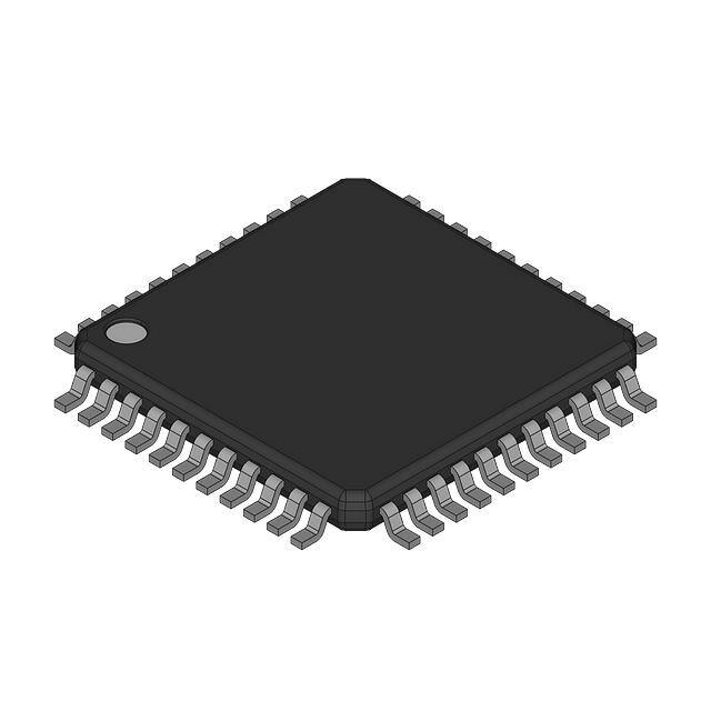
FEATURES Specified for V DD of 3 V to 5.5 V AD7859–200 kSPS; AD7859L–100 kSPS System and Self-Calibration Low Power Normal Operation AD7859: 15 mW (VDD = 3 V) AD7859L: 5.5 mW (V DD = 3 V) Using Automatic Power-Down After Conversion (25 W) AD7859: 1.3 mW (VDD = 3 V 10 kSPS) AD7859L: 650 W (VDD = 3 V 10 kSPS) Flexible Parallel Interface: 16-Bit Parallel/8-Bit Parallel 44-Pin PQFP and PLCC Packages APPLICATIONS Battery-Powered Systems (Personal Digital Assistants, Medical Instruments, Mobile Communications) Pen Computers Instrumentation and Control Systems High Speed Modems GENERAL DESCRIPTION
3 V to 5 V Single Supply, 200 kSPS 8-Channel, 12-Bit Sampling ADCs AD7859/AD7859L*
FUNCTIONAL BLOCK DIAGRAM
AVDD AGND AIN1 I/P MUX AIN8 2.5V REFERENCE COMP REFIN/ REFOUT BUF DGND T/H DVDD
AD7859/AD7859L
CREF1
CHARGE REDISTRIBUTION DAC CLKIN
CREF2 CALIBRATION MEMORY AND CONTROLLER CAL
SAR + ADC CONTROL
CONVST BUSY SLEEP
PARALLEL INTERFACE/CONTROL REGISTER
The AD7859/AD7859L are high speed, low power, 8-channel, 12-bit ADCs which operate from a single 3 V or 5 V power supply, the AD7859 being optimized for speed and the AD7859L for low power. The ADC contains self-calibration and system calibration options to ensure accurate operation over time and temperature and have a number of power-down options for low power applications. The AD7859 is capable of 200 kHz throughput rate while the AD7859L is capable of 100 kHz throughput rate. The input track-and-hold acquires a signal in 500 ns and features a pseudodifferential sampling scheme. The AD7859 and AD7859L input voltage range is 0 to VREF (unipolar) and –VREF/2 to +VREF/2 about VREF/2 (bipolar) with both straight binary and 2s complement output coding respectively. Input signal range is to the supply and the part is capable of converting full-power signals to 100 kHz. CMOS construction ensures low power dissipation of typically 5.4 mW for normal operation and 3.6 µW in power-down mode. The part is available in 44-pin, plastic quad flatpack package (PQFP) and plastic lead chip carrier (PLCC).
*Patent pending. See page 28 for data sheet index.
DB15 – DB0
RD
CS
WR
W/B
PRODUCT HIGHLIGHTS
1. Operation with either 3 V or 5 V power supplies. 2. Flexible power management options including automatic power-down after conversion. 3. By using the power management options a superior power performance at slower throughput rates can be achieved. AD7859: 1 mW typ @ 10 kSPS AD7859L: 1 mW typ @ 20 kSPS 4. Operates with reference voltages from 1.2 V to the supply. 5. Analog input ranges from 0 V to VDD. 6. Self and system calibration. 7. Versatile parallel I/O port. 8. Lower power version AD7859L.
REV. A
Information furnished by Analog Devices is believed to be accurate and reliable. However, no responsibility is assumed by Analog Devices for its use, nor for any infringements of patents or other rights of third parties which may result from its use. No license is granted by implication or otherwise under any patent or patent rights of Analog Devices. © Analog Devices, Inc., 1996 One Technology Way, P.O. Box 9106, Norwood, MA 02062-9106, U.S.A. Tel: 617/329-4700 Fax: 617/326-8703
�( = .5 AD7859/AD7859L–SPECIFICATIONS1,12MHzAV(–40= CDVto +85+3.0 Vf to +5.5 2V,00REF /REF = 2100VkHz External Reference, f = 4 MHz (for L Version: 1.8 MHz (0 C to +70 C) and C)); = kHz (AD7859)
DD DD IN OUT CLKIN SAMPLE
(AD7859L); SLEEP = Logic High; TA = TMIN to TMAX, unless otherwise noted.) Specifications in () apply to the AD7859L.
Parameter DYNAMIC PERFORMANCE Signal to Noise + Distortion Ratio3 (SNR) Total Harmonic Distortion (THD) Peak Harmonic or Spurious Noise Intermodulation Distortion (IMD) Second Order Terms Third Order Terms Channel-to-Channel Isolation DC ACCURACY Resolution Integral Nonlinearity Differential Nonlinearity Unipolar Offset Error Unipolar Offset Error Match Positive Full-Scale Error Negative Full-Scale Error Full-Scale Error Match Bipolar Zero Error Bipolar Zero Error Match ANALOG INPUT Input Voltage Ranges A Version1 B Version1 Units Test Conditions/Comments
70
71
dB min
–78 –78
–78 –78
dB max dB max
Typically SNR is 72 dB VIN = 10 kHz Sine Wave, fSAMPLE = 200 kHz (for L Version: fSAMPLE = 100 kHz @ fCLKIN = 2 MHz) VIN = 10 kHz Sine Wave, fSAMPLE = 200 kHz (for L Version: fSAMPLE = 100 kHz @ fCLKIN = 2 MHz) VIN = 10 kHz Sine Wave, fSAMPLE = 200 kHz (for L Version: fSAMPLE = 100 kHz @ fCLKIN = 2 MHz) fa = 9.983 kHz, fb = 10.05 kHz, fSAMPLE = 200 kHz (for L Version: fSAMPLE = 100 kHz @ fCLKIN = 2 MHz) fa = 9.983 kHz, fb = 10.05 kHz, fSAMPLE = 200 kHz (for L Version: fSAMPLE = 100 kHz @ fCLKIN = 2 MHz) VIN = 25 kHz
–78 –78 –80
–78 –78 –80
dB typ dB typ dB typ
12 ±1 ±1 ±5 ±2 2(3) ±5 ±2 ±2 1 ±1 2
12 ± 0.5 ±1 ±5 ±2 2 ±5 ±2 ±2 1 ±1 2
Bits LSB max LSB max LSB max LSB typ LSB max LSB max LSB typ LSB max LSB max LSB typ LSB typ
5 V Reference VDD = 5 V Guaranteed No Missed Codes to 12 Bits
0 to VREF ± VREF/2 ±1 20
0 to VREF ± VREF/2 ±1 20
Volts Volts
i.e., AIN(+) – AIN(–) = 0 to VREF, AIN(–) Can Be Biased Up But AIN(+) Cannot Go Below AIN(–) i.e., AIN(+) – AIN(–) = –VREF/2 to +VREF/2, AIN(–) Should Be Biased to +VREF/2 and AIN(+) Can Go Below AIN(–) But Cannot Go Below 0 V
Leakage Current Input Capacitance REFERENCE INPUT/OUTPUT REFIN Input Voltage Range Input Impedance REFOUT Output Voltage REFOUT Tempco LOGIC INPUTS Input High Voltage, VINH CAL Pin Input Low Voltage, VINL Input Current, IIN Input Capacitance, CIN4 LOGIC OUTPUTS Output High Voltage, VOH Output Low Voltage, VOL Floating State Leakage Current Floating-State Output Capacitance4 Output Coding
µA max pF typ
2.3/VDD 150 2.3/2.7 20
2.3/VDD 150 2.3/2.7 20
V min/max kΩ typ V min/max ppm/°C typ V min V min V min V min V max V max µA max pF max
Functional from 1.2 V
2.4 2.1 3 2.4 0.8 0.6 ± 10 10
2.4 2.1 3 2.4 0.8 0.6 ± 10 10
AVDD = DVDD = 4.5 V to 5.5 V AVDD = DVDD = 3.0 V to 3.6 V AVDD = DVDD = 4.5 V to 5.5 V AVDD = DVDD = 3.0 V to 3.6 V AVDD = DVDD = 4.5 V to 5.5 V AVDD = DVDD = 3.0 V to 3.6 V Typically 10 nA, VIN = 0 V or VDD
4 2.4 0.4 ± 10 10
4 V min 2.4 V min 0.4 V max ± 10 µA max 10 pF max Straight (Natural) Binary 2s Complement
AVDD = DVDD = 4.5 V to 5.5 V AVDD = DVDD = 3.0 V to 3.6 V ISINK = 1.6 mA
Unipolar Input Range Bipolar Input Range
–2–
REV. A
�AD7859/AD7859L
Parameter CONVERSION RATE Conversion Time Track/Hold Acquisition Time A Version1 B Version1 Units µs max µs min Test Conditions/Comments tCLKIN × 18 (L Versions Only, 0°C to +70°C, 1.8 MHz CLKIN) (L Versions Only, –40°C to +85°C, 1.8 MHz CLKIN) 4.5 (10) 0.5 (1) 4.5 0.5
POWER REQUIREMENTS AVDD, DVDD IDD Normal Mode5 Sleep Mode6 With External Clock On
+3.0/+5.5 5.5 (1.95) 5.5 (1.95) 10 400
+3.0/+5.5 5.5 5.5 10 400 5 200 30 (10) 20 (6.5) 55 36 27.5 18
V min/max mA max mA max µA typ µA typ µA max µA typ mW max mW max µW typ µW typ µW max µW max AVDD = DVDD = 4.5 V to 5.5 V. Typically 4.5 mA AVDD = DVDD = 3.0 V to 3.6 V. Typically 4.0 mA Full Power-Down. Power Management Bits in Control Register Set as PMGT1 = 1, PMGT0 = 0. Partial Power-Down. Power Management Bits in Control Register Set as PMGT1 = 1, PMGT0 = 1. Typically 1 µA. Full Power-Down. Power Management Bits in Control Register Set as PMGT1 = 1, PMGT0 = 0. Partial Power-Down. Power Management Bits in Control Register Set as PMGT1 = 1, PMGT0 = 1. VDD = 5.5 V: Typically 25 mW (8); SLEEP = VDD VDD = 3.6 V: Typically 15 mW (5.4); SLEEP = VDD VDD = 5.5 V; SLEEP = 0 V VDD = 3.6 V; SLEEP = 0 V VDD = 5.5 V: Typically 5.5 µW; SLEEP = 0 V VDD = 3.6 V: Typically 3.6 µW; SLEEP = 0 V Allowable Offset Voltage Span for Calibration Allowable Full-Scale Voltage Span for Calibration
With External Clock Off
5 200
Normal Mode Power Dissipation Sleep Mode Power Dissipation With External Clock On With External Clock Off
30 (10) 20 (6.5) 55 36 27.5 18
SYSTEM CALIBRATION Offset Calibration Span7 Gain Calibration Span7
+0.05 × VREF/–0.05 × VREF V max/min +1.025 × VREF/–0.975 × VREF V max/min
NOTES 1 Temperature range as follows: A, B Versions, –40°C to +85°C. 2 Specifications apply after calibration. 3 SNR calculation includes distortion and noise components. 4 Not production tested, guaranteed by characterization at initial product release. 5 All digital inputs @ DGND except for CONVST , SLEEP, CAL, and SYNC @ DVDD. No load on the digital outputs. Analog inputs @ AGND. 6 CLKIN @ DGND when external clock off. All digital inputs @ DGND except for CONVST, SLEEP, CAL, and SYNC @ DVDD. No load on the digital outputs. Analog inputs @ AGND. 7 The offset and gain calibration spans are defined as the range of offset and gain errors that the AD7859/AD7859L can calibrate. Note also that these are voltage spans and are not absolute voltages (i.e., the allowable system offset voltage presented at AIN(+) for the system offset error to be adjusted out will be AIN(–) ± 0.05 × VREF, and the allowable system full-scale voltage applied between AIN(+) and AIN(–) for the system full-scale voltage error to be adjusted out will be VREF ± 0.025 × VREF). This is explained in more detail in the calibration section of the data sheet. Specifications subject to change without notice.
REV. A
–3–
�AD7859/AD7859L TIMING SPECIFICATIONS
Parameter fCLKIN2 t1 3 t2 tCONVERT t3 t4 t5 t6 t7 t8 4 t9 5 t10 t11 t12 t13 t14 t15 t16 t17 t184 t19 tCAL6 tCAL16 tCAL26 5V
1 (AVDD = DVDD = +3.0 V to +5.5 V; fCLKIN = 4 MHz for AD7859 and 1.8 MHz for AD7859L;
TA = TMIN to TMAX, unless otherwise noted)
Limit at TMIN, TMAX (A, B Versions) 3V 500 4 1.8 100 90 4.5 10 15 5 0 0 55 50 5 40 70 0 5 0 0 70 10 5 1/2 tCLKIN 2.5 tCLKIN 31.25 27.78 3.47
Units kHz min MHz max MHz max ns min ns max µs max µs max ns min ns min ns min ns min ns min ns max ns min ns max ns min ns min ns max ns min ns max ns min ns min ns min ns min ns max ms typ ms typ ms typ
Description Master Clock Frequency L Version CONVST Pulse Width CONVST to BUSY ↑ Propagation Delay Conversion Time = 18 tCLKIN L Version 1.8 MHz CLKIN. Conversion Time = 18 tCLKIN HBEN to RD Setup Time HBEN to RD Hold Time CS to RD to Setup Time CS to RD Hold Time RD Pulse Width Data Access Time After RD Bus Relinquish Time After RD Bus Relinquish Time After RD Minimum Time Between Reads HBEN to WR Setup Time HBEN to WR Hold Time CS to WR Setup Time CS to WR Hold Time WR Pulse Width Data Setup Time Before WR Data Hold Time After WR New Data Valid Before Falling Edge of BUSY CS ↑ to BUSY ↑ in Calibration Sequence Full Self-Calibration Time, Master Clock Dependent (125013 tCLKIN) Internal DAC Plus System Full-Scale Cal Time, Master Clock Dependent (111124 tCLKIN) System Offset Calibration Time, Master Clock Dependent (13889 tCLKIN)
500 4 1.8 100 50 4.5 10 15 5 0 0 55 50 5 40 60 0 5 0 0 55 10 5 1/2 tCLKIN 2.5 tCLKIN 31.25 27.78 3.47
NOTES 1 Sample tested at +25 °C to ensure compliance. All input signals are specified with tr = tf = 5 ns (10% to 90% of V DD) and timed from a voltage level of 1.6 V. 2 Mark/Space ratio for the master clock input is 40/60 to 60/40. 3 The CONVST pulse width will here only apply for normal operation. When the part is in power-down mode, a different CONVST pulse width will apply (see PowerDown section). 4 Measured with the load circuit of Figure 1 and defined as the time required for the output to cross 0.8 V or 2.4 V. 5 t9 is derived form the measured time taken by the data outputs to change 0.5 V when loaded with the circuit of Figure 1. The measured number is then extrapolated back to remove the effects of charging or discharging the 50 pF capacitor. This means that the time, t 9, quoted in the timing characteristics is the true bus relinquish time of the part and is independent of the bus loading. 6 The typical time specified for the calibration times is for a master clock of 4 MHz. For the L version the calibration times will be longer than those quoted here due to the 1.8 MHz master clock. Specifications subject to change without notice.
–4–
REV. A
�AD7859/AD7859L
ABSOLUTE MAXIMUM RATINGS 1
1.6mA IOL
(TA = +25°C unless otherwise noted)
TO OUTPUT PIN 50pF
+2.1V
200µA
IOH
Figure 1. Load Circuit for Digital Output Timing Specifications
ORDERING GUIDE
Model
Linearity Error (LSB)1
Power Dissipation Package (mW) Option2 15 15 15 5.5 P-44A S-44 S-44 S-44
AD7859AP ±1 AD7859AS ±1 AD7859BS ± 1/2 AD7859LAS3 ±1 EVAL-AD7859CB4 EVAL-CONTROL BOARD5
NOTES 1 Linearity error refers to the integral linearity error. 2 P = PLCC; S = PQFP. 3 L signifies the low power version. 4 This can be used as a stand-alone evaluation board or in conjunction with the EVAL-CONTROL BOARD for evaluation/demonstration purposes. 5 This board is a complete unit allowing a PC to control and communicate with all Analog Devices, Inc. evaluation boards ending in the CB designators. For more information on Analog Devices products and evaluation boards, visit our World Wide Web home page at http://www.analog.com.
AVDD to AGND . . . . . . . . . . . . . . . . . . . . . . . . –0.3 V to +7 V DVDD to DGND . . . . . . . . . . . . . . . . . . . . . . . –0.3 V to +7 V AVDD to DVDD . . . . . . . . . . . . . . . . . . . . . . . –0.3 V to +0.3 V Analog Input Voltage to AGND . . . . –0.3 V to AVDD + 0.3 V Digital Input Voltage to DGND . . . . –0.3 V to DVDD + 0.3 V Digital Output Voltage to DGND . . . –0.3 V to DVDD + 0.3 V REFIN/REFOUT to AGND . . . . . . . . . –0.3 V to AVDD + 0.3 V Input Current to Any Pin Except Supplies2 . . . . . . . . ± 10 mA Operating Temperature Range Commercial (A, B Versions) . . . . . . . . . . . –40°C to +85°C Storage Temperature Range . . . . . . . . . . . –65°C to +150°C Junction Temperature . . . . . . . . . . . . . . . . . . . . . . . . . +150°C PQFP Package, Power Dissipation . . . . . . . . . . . . . . 450 mW θJA Thermal Impedance . . . . . . . . . . . . . . . . . . . . . 95°C/W Lead Temperature, Soldering Vapor Phase (60 sec) . . . . . . . . . . . . . . . . . . . . . . +215°C Infrared (15 sec) . . . . . . . . . . . . . . . . . . . . . . . . . . +220°C PLCC Package, Power Dissipation . . . . . . . . . . . . . . 500 mW θJA Thermal Impedance . . . . . . . . . . . . . . . . . . . . . . . 55°C/W Lead Temperature, Soldering Vapor Phase (60 sec) . . . . . . . . . . . . . . . . . . . . . . +215°C Infrared (15 sec) . . . . . . . . . . . . . . . . . . . . . . . . . . +220°C ESD . . . . . . . . . . . . . . . . . . . . . . . . . . . . . . . . . . . . . >1500 kV
NOTES 1 Stresses above those listed under “Absolute Maximum Ratings” may cause permanent damage to the device. This is a stress rating only and functional operation of the device at these or any other conditions above those listed in the operational sections of this specification is not implied. Exposure to absolute maximum rating conditions for extended periods may affect device reliability. 2 Transient currents of up to 100 mA will not cause SCR latchup.
PINOUT FOR PLCC
CONVST CLKIN BUSY
PINOUT FOR PQFP
CONVST BUSY CLKIN
DB15
DB14
DB13
DB15
DB14
DB13
DB12
WR
DB12
35
RD
CS
WR
CS
RD
44
43
42
39
38
36
41
NC W/B REFIN/REFOUT
7 8 9
39 NC 38 DB11
NC W/B
1 2 3 4 5 6 7 8 9 10 11
40
37
34
6
5
4
3
2
1
44
43
42
41 40
NC
NC
33 32 31 30
PIN NO. 1 IDENTIFIER
NC DB11 DB10 DB9 DB8/HBEN DGND DVDD DB7 DB6 DB5 DB4
37 DB10 36 DB9
AVDD 10 AGND 11 CREF1 12 CREF2 13 AIN0 14 AIN1 15 AIN2 16 AIN3 17
18 19 20 21 22 23 24 25 26 27 28
REFIN/REFOUT AVDD AGND CREF1 CREF2 AIN0 AIN1 AIN2 AIN3
AD7859
TOP VIEW (Not to Scale)
35 DB8/HBEN 34 DGND 33 DVDD 32 DB7 31 DB6 30 DB5 29 DB4
AD7859
TOP VIEW (Not to Scale)
29 28 27 26 25 24 23
AIN6
AIN7
DB1
DB2
DB0
DB3
AIN4
AIN5
SLEEP
CAL
NC
15
14
16
20
12
17
21
13
18
AIN6
AIN7
DB0
DB1
19
DB2
DB3
AIN4
AIN5
REV. A
–5–
SLEEP
CAL
NC
22
�AD7859/AD7859L
TERMINOLOGY Integral Nonlinearity
This is the maximum deviation from a straight line passing through the endpoints of the ADC transfer function. The endpoints of the transfer function are zero scale, a point 1/2 LSB below the first code transition, and full scale, a point 1/2 LSB above the last code transition. Differential Nonlinearity This is the difference between the measured and the ideal 1 LSB change between any two adjacent codes in the ADC. Unipolar Offset Error This is the deviation of the first code transition (00 . . . 000 to 00 . . . 001) from the ideal AIN(+) voltage (AIN(–) + 1/2 LSB) when operating in the unipolar mode. Positive Full-Scale Error This applies to the unipolar and bipolar modes and is the deviation of the last code transition from the ideal AIN(+) voltage (AIN(–) + Full Scale – 1.5 LSB) after the offset error has been adjusted out. Negative Full-Scale Error This applies to the bipolar mode only and is the deviation of the first code transition (10 . . . 000 to 10 . . . 001) from the ideal AIN(+) voltage (AIN(–) – VREF/2 + 0.5 LSB). Bipolar Zero Error This is the deviation of the midscale transition (all 0s to all 1s) from the ideal AIN(+) voltage (AIN(–) – 1/2 LSB). Track/Hold Acquisition Time The track/hold amplifier returns into track mode and the end of conversion. Track/Hold acquisition time is the time required for the output of the track/hold amplifier to reach its final value, within ± 1/2 LSB, after the end of conversion. Signal to (Noise + Distortion) Ratio This is the measured ratio of signal to (noise + distortion) at the output of the A/D converter. The signal is the rms amplitude of the fundamental. Noise is the sum of all nonfundamental signals up to half the sampling frequency (fS/2), excluding dc. The ratio is dependent on the number of quantization levels in the digitization process; the more levels, the smaller the quantization noise. The theoretical signal to (noise + distortion) ratio for an ideal N-bit converter with a sine wave input is given by: Signal to (Noise + Distortion) = (6.02 N +1.76) dB Thus for a 12-bit converter, this is 74 dB.
Total Harmonic Distortion Total harmonic distortion (THD) is the ratio of the rms sum of harmonics to the fundamental. For the AD7859/AD7859L, it is defined as: THD ( dB ) = 20 log (V 2 + V 3 + V 4 + V 5 + V 6 ) V1
2 2 2 2 2
where V1 is the rms amplitude of the fundamental and V2, V3, V4, V5 and V6 are the rms amplitudes of the second through the sixth harmonics. Peak Harmonic or Spurious Noise Peak harmonic or spurious noise is defined as the ratio of the rms value of the next largest component in the ADC output spectrum (up to fS/2 and excluding dc) to the rms value of the fundamental. Normally, the value of this specification is determined by the largest harmonic in the spectrum, but for parts where the harmonics are buried in the noise floor, it will be a noise peak. Intermodulation Distortion With inputs consisting of sine waves at two frequencies, fa and fb, any active device with nonlinearities will create distortion products at sum and difference frequencies of mfa ± nfb where m, n = 0, 1, 2, 3, etc. Intermodulation distortion terms are those for which neither m nor n are equal to zero. For example, the second order terms include (fa + fb) and (fa – fb), while the third order terms include (2fa + fb), (2fa – fb), (fa + 2fb) and (fa – 2fb). Testing is performed using the CCIF standard where two input frequencies near the top end of the input bandwidth are used. In this case, the second order terms are usually distanced in frequency from the original sine waves while the third order terms are usually at a frequency close to the input frequencies. As a result, the second and third order terms are specified separately. The calculation of the intermodulation distortion is as per the THD specification where it is the ratio of the rms sum of the individual distortion products to the rms amplitude of the sum of the fundamentals expressed in dBs.
–6–
REV. A
�AD7859/AD7859L
PIN FUNCTION DESCRIPTION
Mnemonic CONVST RD WR CS REFIN/ REFOUT
Description Convert Start. Logic input. A low to high transition on this input puts the track/hold into its hold mode and starts conversion. When this input is not used, it should be tied to DVDD. Read Input. Active low logic input. Used in conjunction with CS to read from internal registers. Write Input. Active low logic input. Used in conjunction with CS to write to internal registers. Chip Select Input. Active low logic input. The device is selected when this input is active. Reference Input/Output. This pin is connected to the internal reference through a series resistor and is the reference source for the analog-to-digital converter. The nominal reference voltage is 2.5 V and this appears at the pin. This pin can be overdriven by an external reference or can be taken as high as AVDD. When this pin is tied to AVDD, then the CREF1 pin should also be tied to AVDD. Analog Supply Voltage, +3.0 V to +5.5 V. Analog Ground. Ground reference for track/hold, reference and DAC. Digital Supply Voltage, +3.0 V to +5.5 V. Digital Ground. Ground reference point for digital circuitry. Reference Capacitor (0.1 µF multilayer ceramic). This external capacitor is used as a charge source for the internal DAC. The capacitor should be tied between the pin and AGND. Reference Capacitor (0.01 µF ceramic disc). This external capacitor is used in conjunction with the on-chip reference. The capacitor should be tied between the pin and AGND. Analog Inputs. Eight analog inputs which can be used as eight single ended inputs (referenced to AGND) or four pseudo differential inputs. Channel configuration is selected by writing to the control register. None of the inputs can go below AGND or above AVDD at any time. See Table III for channel selection. Word/Byte input. When this input is at a logic 1, data is transferred to and from the AD7859/AD7859L in 16-bit words on pins DB0 to DB15. When this pin is at a Logic 0, byte transfer mode is enabled. Data is transferred on pins DB0 to DB7 and pin DB8/HBEN assumes its HBEN functionality. Data Bits 0 to 7. Three state data I/O pins that are controlled by CS, RD and WR. Data output is straight binary (unipolar mode) or twos complement (bipolar mode). Data Bit 8/High Byte Enable. When W/B is high, this pin acts as Data Bit 7, a three state data I/O pin that is controlled by CS, RD and WR. When W/B is low, this pin acts as the High Byte Enable pin. When HBEN is low, then the low byte of data being written to or read from the AD7859/AD7859L is on DB0 to DB7. When HBEN is high, then the high byte of data being written to or read from the AD7859/AD7859L is on DB0 to DB7. Data Bits 9 to 15. Three state data I/O pins that are controlled by CS, RD and WR. Data output is straight binary (unipolar mode) or twos complement (bipolar mode). Master Clock Signal for the device (4 MHz for AD7859, 1.8 MHz for AD7859L). Sets the conversion and calibration times. Calibration Input. A logic 0 in this pin resets all logic. A rising edge on this pin initiates a calibration. This input overrides all other internal operations. Busy Output. The busy output is triggered high when a conversion or a calibration is initiated, and remains high until the conversion or calibration is completed. Sleep Input. This pin is used in conjunction with the PGMT0 and PGMT1 bits in the control register to determine the power-down mode. Please see the “Power-Down Options” section for details. No connect pins. These pins should be left unconnected.
AVDD AGND DVDD DGND CREF1 CREF2 AIN1–AIN8
W/B
DB0–DB7 DB8/HBEN
DB9–DB15 CLKIN CAL BUSY SLEEP NC
REV. A
–7–
�AD7859/AD7859L
AD7859/AD7859L ON-CHIP REGISTERS
The AD7859/AD7859L powers up with a set of default conditions. The only writing that is required is to select the channel configuration. Without performing any other write operations, the AD7859/AD7859L still retains the flexibility for performing a full powerdown and a full self-calibration. Extra features and flexibility such as performing different power-down options, different types of calibrations, including system calibration, and software conversion start can be selected by writing to the part. The AD7859/AD7859L contains a Control register, ADC output data register, Status register, Test register and 10 Calibration registers. The control register is write-only, the ADC output data register and the status register are read-only, and the test and calibration registers are both read/write registers. The test register is used for testing the part and should not be written to.
Addressing the On-Chip Registers
Writing When writing to the AD7859/AD7859L, a 16-bit word of data must be transferred. The 16 bits of data is written as either a 16-bit word, or as two 8-bit bytes, depending on the logic level at the W/B pin. When W/B is high, the 16 bits are transferred on DB0 to DB15, where DB0 is the LSB and DB15 is the MSB of the write. When W/B is low, DB8/HBEN assumes its HBEN functionality and data is transferred in two 8-bit bytes on pins DB0 to DB7, pin DB0 being the LSB of each transfer and pin DB7 being the MSB. When writing to the AD7859/AD7859L in byte mode, the low byte must be written first followed by the high byte. The two MSBs of the complete 16-bit word, ADDR1 and ADDR0, are decoded to determine which register is addressed, and the 14 LSBs are written to the addressed register. Table I shows the decoding of the address bits, while Figure 2 shows the overall write register hierarchy.
Table I. Write Register Addressing
ADDR1 0 0 1 1
ADDR0 0 1 0 1
Comment This combination does not address any register. This combination addresses the TEST REGISTER. The 14 LSBs of data are written to the test register. This combination addresses the CALIBRATION REGISTERS. The 14 LSBs of data are written to the selected calibration register. This combination addresses the CONTROL REGISTER. The 14 LSBs of data are written to the control register.
Reading To read from the various registers the user must first write to Bits 6 and 7 in the Control Register, RDSLT0 and RDSLT1. These bits are decoded to determine which register is addressed during a read operation. Table II shows the decoding of the read address bits while Figure 3 shows the overall read register hierarchy. The power-up status of these bits is 00 so that the default read will be from the ADC output data register. As with writing to the AD7859/AD7859L either word or byte mode can be used. When reading from the calibration registers in byte mode, the low byte must be read first. Once the read selection bits are set in the control register all subsequent read operations that follow are from the selected register until the read selection bits are changed in the control register.
Table II. Read Register Addressing
RDSLT1 0 0 1 1
RDSLT0 0 1 0 1
Comment All successive read operations are from the ADC OUTPUT DATA REGISTER. This is the default powerup setting. There is always four leading zeros when reading from the ADC output data register. All successive read operations are from the TEST REGISTER. All successive read operations are from the CALIBRATION REGISTERS. All successive read operations are from the STATUS REGISTER.
ADDR1, ADDR0 DECODE 01 TEST REGISTER 10 CALIBRATION REGISTERS 11 CONTROL REGISTER 00 ADC OUTPUT DATA REGISTER 01 TEST REGISTER RDSLT1, RDSLT0 DECODE 10 CALIBRATION REGISTERS 11 STATUS REGISTER
GAIN (1) OFFSET (1) DAC (8) CALSLT1, CALSLT0 DECODE 00
GAIN (1) OFFSET (1) 01
OFFSET (1)
GAIN (1)
GAIN (1) OFFSET (1) DAC (8) CALSLT1, CALSLT0 DECODE 00
GAIN (1) OFFSET (1) 01
OFFSET (1)
GAIN (1)
10
11
10
11
Figure 2. Write Register Hierarchy/Address Decoding
Figure 3. Read Register Hierarchy/Address Decoding
–8–
REV. A
�AD7859/AD7859L
CONTROL REGISTER
The arrangement of the control register is shown below. The control register is a write only register and contains 14 bits of data. The control register is selected by putting two 1s in ADDR1 and ADDR0. The function of the bits in the control register is described below. The power-up status of all bits is 0. MSB SGL/DIFF RDSLT0 CHSLT2 AMODE CHSLT1 CONVST CHSLT0 CALMD PMGT1 CALSLT1 PMGT0 CALSLT0 RDSLT1 STCAL LSB
CONTROL REGISTER BIT FUNCTION DESCRIPTION
Bit 13 12 11 10 9 8 7 6 5
Mnemonic SGL/DIFF CHSLT2 CHSLT1 CHSLT0 PMGT1 PMGT0 RDSLT1 RDSLT0 AMODE
Comment A 0 in this bit position configures the input channels for pseudo-differential mode. A 1 in this bit position configures the input channels in single ended mode. Please see Table III for channel selection. These three bits are used to select the analog input on which the conversion is performed. The analog inputs can be configured as eight single-ended channels or four pseudo-differential channels. The default selection is AIN1 for the positive input and AIN2 for the negative input. Please see Table III for channel selection information. Power Management Bits. These two bits are used with the SLEEP pin for putting the part into various Power-Down modes (See Power-Down section for more details). Theses two bits determine which register is addressed for the read operations. Please see Table II. Analog Mode Bit. This bit has two different functions, depending on the status of the SGL/DIFF bit. When SGL/DIFF is 0, AMODE selects between unipolar and bipolar analog input ranges. A logic 0 in this bit position selects the unipolar range, 0 to VREF (i.e., AIN(+) – AIN(–) = 0 to VREF). A logic 1 in this bit position selects the bipolar range –VREF/2 to +VREF/2 (i.e., AIN(+) – AIN(–) = –VREF /2 to +VREF/2). In this case AIN(–) needs to be tied to at least +VREF/2 to allow AIN(+) to have a full input swing from 0 V to +VREF. When SGL/DIFF is 1, AMODE selects the source for the AIN(–) channel of the sample and hold circuitry. If AMODE is a 0, AGND is selected. If AMODE is a 1, then AIN8 is selected. Please see Table III for more information. Conversion Start Bit. A logic 1 in this bit position starts a single conversion, and this bit is automatically reset to 0 at the end of conversion. This bit may also be used in conjunction with system calibration (see calibration section on page 21). Calibration Mode Bit. A 0 here selects self-calibration and a 1 selects a system calibration (see Table IV). Calibration Selection Bits 1 and 0. These bits have two functions, depending on the STCAL bit. With the STCAL bit set to 1, the CALSLT1 and CALSLT0 bits, along with the CALMD bit, determine the type of calibration performed by the part (see Table IV). With the STCAL bit set to 0, the CALSLT1 and CALSLT0 bits are decoded to address the calibration register for read/write of calibration coefficients (see Table V for more details). Start Calibration Bit. When STCAL is set to a 1, a calibration is performed, as determined by the CALMD, CALSLT1 and CALSLT0 bits. Please see Table IV. When STCAL is set to a zero, no calibration is performed.
4
CONVST
3 2 1
CALMD CALSLT1 CALSLT0
0
STCAL
REV. A
–9–
�AD7859/AD7859L
Table IIIa. Channel Selection for AD7859/AD7859L Differential Sampling (SGL/DIFF = 0) Table IIIb. Channel Selection for AD7859/AD7859L Single-Ended Sampling (SGL/DIFF = 1)
AMODE 0 0 0 0 0 1 1 1 1 1
CHSLT 210 0 0 0 0 1 0 0 0 0 1 0 0 1 1 x 0 0 1 1 x 0 1 0 1 x 0 1 0 1 x
AIN(+)*AIN(–)* AIN1 AIN3 AIN5 AIN7 x AIN1 AIN3 AIN5 AIN7 x AIN2 AIN4 AIN6 AIN8 x AIN2 AIN4 AIN6 AIN8 x
Bipolar or Unipolar Unipolar Unipolar Unipolar Unipolar Not Used Bipolar Bipolar Bipolar Bipolar Not Used
AMODE 0 0 0 0 0 0 0 0 1 1 1 1 1 1 1 1
CHSLT 210 0 0 0 0 1 1 1 1 0 0 0 0 1 1 1 1 0 0 1 1 0 0 1 1 0 0 1 1 0 0 1 1 0 1 0 1 0 1 0 1 0 1 0 1 0 1 0 1
AIN(+)*AIN(–)* AIN1 AIN3 AIN5 AIN7 AIN2 AIN4 AIN6 AIN8 AIN1 AIN3 AIN5 AIN7 AIN2 AIN4 AIN6 AIN8 AGND AGND AGND AGND AGND AGND AGND AGND AIN8 AIN8 AIN8 AIN8 AIN8 AIN8 AIN8 AIN8
Bipolar or Unipolar Unipolar Unipolar Unipolar Unipolar Unipolar Unipolar Unipolar Unipolar Unipolar Unipolar Unipolar Unipolar Unipolar Unipolar Unipolar Unipolar
*AIN(+) refers to the positive input seen by the AD7859/AD7859L sample-andhold circuitry. AIN(–) refers to the negative input seen by the AD7859/AD7859L sample-andhold circuitry.
Table IV. Calibration Selection
CALMD 0 0 0 0 1 1 1 1
CALSLT1 0 0 1 1 0 0 1 1
CALSLT0 0 1 0 1 0 1 0 1
Calibration Type A full internal calibration is initiated. First the internal DAC is calibrated, then the internal gain error and finally the internal offset error are removed. This is the default setting. First the internal gain error is removed, then the internal offset error is removed. The internal offset error only is calibrated out. The internal gain error only is calibrated out. A full system calibration is initiated. First the internal DAC is calibrated, followed by the system gain error calibration, and finally the system offset error calibration. First the system gain error is calibrated out, followed by the system offset error. The system offset error only is removed. The system gain error only is removed.
–10–
REV. A
�AD7859/AD7859L
STATUS REGISTER
The arrangement of the status register is shown below. The status register is a read-only register and contains 16 bits of data. The status register is selected by first writing to the control register and putting two 1s in RDSLT1 and RDSLT0. The function of the bits in the status register are described below. The power-up status of all bits is 0.
START
WRITE TO CONTROL REGISTER SETTING RDSLT0 = RDSLT1 = 1
READ STATUS REGISTER
Figure 4. Flowchart for Reading the Status Register
MSB ZERO ONE ZERO ONE SGL/DIFF AMODE CHSLT2 BUSY CHSLT1 CALMD CHSLT0 CALSLT1 PMGT1 CALSLT0 PMGT0 STCAL LSB
STATUS REGISTER BIT FUNCTION DESCRIPTION
Bit 15 14 13 12 11 10 9 8 7 6 5
Mnemonic ZERO ZERO SGL/DIFF CHSLT2 CHSLT1 CHSLT0 PMGT1 PMGT0 ONE ONE AMODE
Comment These two bits are always 0. Single/Differential Bit. Channel Selection Bits. These bits, in conjunction with the SGL/DIFF bit, determine which channel has been selected for conversion. Please refer to Table IIIa and Table IIIb. Power Management Bits. These bits along with the SLEEP pin indicate if the part is in a power-down mode or not. See Table VI in Power-Down Section for description. Both these bits are always 1. Analog Mode Bit. This bit is used along with SGL/DIFF and CHSLT2 – CHSLT0 to determine the AIN(+) and AIN(–) inputs to the track and hold circuitry and the analog conversion mode (unipolar or bipolar). Please see Table III for details. Conversion/Calibration BUSY Bit. When this bit is a 1, there is a conversion or a calibration in progress. When this bit is a zero, there is no conversion or calibration in progress. Calibration Mode Bit. A 0 in this bit indicates a self-calibration is selected, and a 1 in this bit indicates a system calibration is selected (see Table IV). Calibration Selection Bits. The CALSLT1 and CALSLT0 bits indicate which of the calibration registers are addressed for reading and writing (see section on the Calibration Registers for more details). Start Calibration Bit. The STCAL bit is a 1 if a calibration is in progress and a 0 if there is no calibration in progress.
4 3 2 1 0
BUSY CALMD CALSLT1 CALSLT0 STCAL
REV. A
–11–
�AD7859/AD7859L
CALIBRATION REGISTERS
The AD7859/AD7859L has 10 calibration registers in all, 8 for the DAC, 1 for offset and 1 for gain. Data can be written to or read from all 10 calibration registers. In self and system calibration, the part automatically modifies the calibration registers; only if the user needs to modify the calibration registers should an attempt be made to read from and write to the calibration registers.
Addressing the Calibration Registers
The calibration selection bits in the control register CALSLT1 and CALSLT0 determine which of the calibration registers are addressed (See Table V). The addressing applies to both the read and write operations for the calibration registers. The user should not attempt to read from and write to the calibration registers at the same time.
Table V. Calibration Register Addressing
CALSLT1 0 0 1 1
CALSLT0 0 1 0 1
Comment This combination addresses the Gain (1), Offset (1) and DAC Registers (8). Ten registers in total. This combination addresses the Gain (1) and Offset (1) Registers. Two registers in total. This combination addresses the Offset Register. One register in total. This combination addresses the Gain Register. One register in total. When reading from the calibration registers there is always two leading zeros for each of the registers.
START
Writing to/Reading from the Calibration Registers
When writing to the calibration registers a write to the control register is required to set the CALSLT0 and CALSLT1 bits. When reading from the calibration registers a write to the control register is required to set the CALSLT0 and CALSLT1 bits and also to set the RDSLT1 and RDSLT0 bits to 10 (this addresses the calibration registers for reading). The calibration register pointer is reset on writing to the control register setting the CALSLT1 and CALSLT0 bits, or upon completion of all the calibration register write/read operations. When reset it points to the first calibration register in the selected write/read sequence. The calibration register pointer points to the gain calibration register upon reset in all but one case, this case being where the offset calibration register is selected on its own (CALSLT1 = 1, CALSLT0 = 0). Where more than one calibration register is being accessed, the calibration register pointer is automatically incremented after each full calibration register write/read operation. The calibration register address pointer is incremented after the high byte read or write operation in byte mode. Therefore when reading (in byte mode) from the calibration registers, the low byte must always be read first, i.e., HBEN = logic zero. The order in which the 10 calibration registers are arranged is shown in Figure 5. Read/Write operations may be aborted at any time before all the calibration registers have been accessed, and the next control register write operation resets the calibration register pointer. The flowchart in Figure 6 shows the sequence for writing to the calibration registers. Figure 7 shows the sequence for reading from the calibration registers.
CALIBRATION REGISTERS CAL REGISTER ADDRESS POINTER GAIN REGISTER OFFSET REGISTER DAC 1st MSB REGISTER (1) (2) (3)
WRITE TO CONTROL REGISTER SETTING STCAL = 0 AND CALSLT1, CALSLT0 = 00, 01, 10, 11
CAL REGISTER POINTER IS AUTOMATICALLY RESET
WRITE TO CAL REGISTER (ADDR1 = 1, ADDR0 = 0)
CAL REGISTER POINTER IS AUTOMATICALLY INCREMENTED
LAST REGISTER WRITE OPERATION OR ABORT ? YES FINISHED
NO
Figure 6. Flowchart for Writing to the Calibration Registers
DAC 8th MSB REGISTER CALIBRATION REGISTER ADDRESS POINTER POSITION IS DETERMINED BY THE NUMBER OF CALIBRATION REGISTERS ADDRESSED AND THE NUMBER OF READ/WRITE OPERATIONS.
(10)
Figure 5. Calibration Register Arrangement
–12–
REV. A
�AD7859/AD7859L
START
WRITE TO CONTROL REGISTER SETTING STCAL = 0, RDSLT1 = 1, RDSLT0 = 0, AND CALSLT1, CALSLT0 = 00, 01, 10, 11
CAL REGISTER POINTER IS AUTOMATICALLY RESET
ence voltage, the MSB-1 has a weighting of 2.5%, the MSB-2 has a weighting of 1.25%, and so on down to the LSB which has a weighting of 0.0006%. This gives a resolution of ± 0.0006% of VREF approximately. The resolution can also be expressed as ± (0.05 × VREF)/213 volts. This equals ± 0.015 mV, with a 2.5 V reference. The maximum offset that can be compensated for is ± 5% of the reference voltage, which equates to ± 125 mV with a 2.5 V reference and ± 250 mV with a 5 V reference. Q. If a +20 mV offset is present in the analog input signal and the reference voltage is 2.5 V, what code needs to be written to the offset register to compensate for the offset ? A. 2.5 V reference implies that the resolution in the offset register is 5% × 2.5 V/213 = 0.015 mV. +20 mV/0.015 mV = 1310.72; rounding to the nearest number gives 1311. In binary terms this is 00 0101 0001 1111, therefore increase the offset register by 00 0101 0001 1111. This method of compensating for offset in the analog input signal allows for fine tuning the offset compensation. If the offset on the analog input signal is known, there is no need to apply the offset voltage to the analog input pins and do a system calibration. The offset compensation can take place in software.
Adjusting the Gain Calibration Register
READ CAL REGISTER
CAL REGISTER POINTER IS AUTOMATICALLY INCREMENTED
LAST REGISTER WRITE OPERATION OR ABORT ? YES FINISHED
NO
Figure 7. Flowchart for Reading from the Calibration Registers
Adjusting the Offset Calibration Register
The offset calibration register contains 16 bits. The two MSBs are zero and the 14 LSBs contain offset data. By changing the contents of the offset register, different amounts of offset on the analog input signal can be compensated for. Decreasing the number in the offset calibration register compensates for negative offset on the analog input signal, and increasing the number in the offset calibration register compensates for positive offset on the analog input signal. The default value of the offset calibration register is 0010 0000 0000 0000 approximately. This is not the exact value, but the value in the offset register should be close to this value. Each of the 14 data bits in the offset register is binary weighted; the MSB has a weighting of 5% of the refer-
The gain calibration register contains 16 bits. The two MSBs are zero and the 14 LSBs contain gain data. As in the offset calibrating register the data bits in the gain calibration register are binary weighted, with the MSB having a weighting of 2.5% of the reference voltage. The gain register value is effectively multiplied by the analog input to scale the conversion result over the full range. Increasing the gain register compensates for a smaller analog input range and decreasing the gain register compensates for a larger input range. The maximum analog input range that the gain register can compensate for is 1.025 times the reference voltage, and the minimum input range is 0.975 times the reference voltage.
REV. A
–13–
�AD7859/AD7859L
CIRCUIT INFORMATION
The AD7859/AD7859L is a fast, 8-channel, 12-bit, single supply A/D converter. The part requires an external 4 MHz/1.8 MHz master clock (CLKIN), two CREF capacitors, a CONVST signal to start conversion and power supply decoupling capacitors. The part provides the user with track/hold, on-chip reference, calibration features, A/D converter and parallel interface logic functions on a single chip. The A/D converter section of the AD7859/AD7859L consists of a conventional successive-approximation converter based around a capacitor DAC. The AD7859/AD7859L accepts an analog input range of 0 to +VREF. VREF can be tied to VDD. The reference input to the part connected via a 150 kΩ resistor to the internal 2.5 V reference and to the on-chip buffer. A major advantage of the AD7859/AD7859L is that a conversion can be initiated in software, as well as by applying a signal to the CONVST pin. The part is available in a 44-pin PLCC or a 44-pin PQFP package, and this offers the user considerable spacing saving advantages over alternative solutions. The AD7859L version typically consumes only 5.5 mW making it ideal for battery-powered applications.
CONVERTER DETAILS
and 1.5 CLKIN periods are allowed for the acquisition time. With a 1.8 MHz clock, this gives a full cycle time of 10 µs, which equates to a throughput rate of 100 kSPS. When using the software conversion start for maximum throughput, the user must ensure the control register write operation extends beyond the falling edge of BUSY. The falling edge of BUSY resets the CONVST bit to 0 and allows it to be reprogrammed to 1 to start the next conversion.
TYPICAL CONNECTION DIAGRAM
Figure 8 shows a typical connection diagram for the AD7859/ AD7859L. The AGND and the DGND pins are connected together at the device for good noise suppression. The first CONVST applied after power-up starts a self-calibration sequence. This is explained in the calibration section of this data sheet. Note that after power is applied to AVDD and DVDD and the CONVST signal is applied, the part requires (70 ms + 1/ sample rate) for the internal reference to settle and for the selfcalibration on power-up to be completed.
4MHz/1.8MHz OSCILLATOR ANALOG SUPPLY +3V TO +5V
10µF
0.1µF
0.1µF CONVERSION START SIGNAL AVDD DVDD W/B CLKIN CONVST
The master clock for the part is applied to the CLKIN pin. Conversion is initiated on the AD7859/AD7859L by pulsing the CONVST input or by writing to the control register and setting the CONVST bit to 1. On the rising edge of CONVST (or at the end of the control register write operation), the on-chip track/hold goes from track to hold mode. The falling edge of the CLKIN signal which follows the rising edge of CONVST initiates the conversion, provided the rising edge of CONVST (or WR when converting via the control register) occurs typically at least 10 ns before this CLKIN edge. The conversion takes 16.5 CLKIN periods from this CLKIN falling edge. If the 10 ns setup time is not met, the conversion takes 17.5 CLKIN periods. The time required by the AD7859/AD7859L to acquire a signal depends upon the source resistance connected to the AIN(+) input. Please refer to the acquisition time section for more details. When a conversion is completed, the BUSY output goes low, and the result of the conversion can be read by accessing the data through the data bus. To obtain optimum performance from the part, read or write operations should not occur during the conversion or less than 200 ns prior to the next CONVST rising edge. Reading/writing during conversion typically degrades the Signal-to-(Noise + Distortion) by less than 0.5 dBs. The AD7859 can operate at throughput rates of over 200 kSPS (up to 100 kSPS for the AD7859L). With the AD7859L, 100 kSPS throughput can be obtained as follows: the CLKIN and CONVST signals are arranged to give a conversion time of 16.5 CLKIN periods as described above
0V TO 2.5V INPUT
AIN(+) AIN(–) CREF1
0.1µF
CS CREF2
0.01µF DVDD
AD7859/ AD7859L
RD WR BUSY DB0 DB15 µC/µP
SLEEP CAL AGND DGND REFIN/REFOUT
0.1nF EXTERNAL REF 0.1µF INTERNAL REF OPTIONAL EXTERNAL REFERENCE
AD780/ REF192
Figure 8. Typical Circuit
For applications where power consumption is a major concern, the power-down options can be exercised by writing to the part and using the SLEEP pin. See the Power-Down section for more details on low power applications.
–14–
REV. A
�AD7859/AD7859L
ANALOG INPUT DC/AC Applications
The equivalent analog input circuit is shown in Figure 9. AIN(+) is the channel connected to the positive input of the track/hold circuitry and AIN(–) is the channel connected to the negative input. Please refer to Table IIIa and Table IIIb for channel configuration. During the acquisition interval the switches are both in the track position and the AIN(+) charges the 20 pF capacitor through the 125 Ω resistance. The rising edge of CONVST switches SW1 and SW2 go into the hold position retaining charge on the 20 pF capacitor as a sample of the signal on AIN(+). The AIN(–) is connected to the 20 pF capacitor, and this unbalances the voltage at node A at the input of the comparator. The capacitor DAC adjusts during the remainder of the conversion cycle to restore the voltage at node A to the correct value. This action transfers a charge, representing the analog input signal, to the capacitor DAC which in turn forms a digital representation of the analog input signal. The voltage on the AIN(–) pin directly influences the charge transferred to the capacitor DAC at the hold instant. If this voltage changes during the conversion period, the DAC representation of the analog input voltage is altered. Therefore it is most important that the voltage on the AIN(–) pin remains constant during the conversion period. Furthermore, it is recommended that the AIN(–) pin is always connected to AGND or to a fixed dc voltage.
125Ω AIN(+) AIN(–) 125Ω HOLD SW1 20pF CAPACITOR DAC TRACK
For dc applications, high source impedances are acceptable, provided there is enough acquisition time between conversions to charge the 20 pF capacitor. For example with RIN = 5 kΩ, the required acquisition time is 922 ns. For ac applications, removing high frequency components greater than the Nyquist frequency from the analog input signal is recommended by use of a low- pass filter on the AIN(+) pin, as shown in Figure 11. In applications where harmonic distortion and signal to noise ratio are critical, the analog input should be driven from a low impedance source. Large source impedances significantly affect the ac performance of the ADC. They may require the use of an input buffer amplifier. The choice of the amplifier is a function of the particular application. The maximum source impedance depends on the amount of total harmonic distortion (THD) that can be tolerated. The THD increases as the source impedance increases. Figure 10 shows a graph of the Total Harmonic Distortion vs. analog input signal frequency for different source impedances. With the setup as in Figure 11, the THD is at the –90 dB level. With a source impedance of 1 kΩ and no capacitor on the AIN(+) pin, the THD increases with frequency.
–72 THD VS. FREQUENCY FOR DIFFERENT SOURCE IMPEDANCES –76
THD – dB
–80
RIN = 1kΩ
NODE A
SW2 COMPARATOR TRACK AGND HOLD
–84
–88
RIN = 50kΩ, 10nF AS IN FIGURE 13
Figure 9. Analog Input Equivalent Circuit
Acquisition Time
–92
0
20
40 60 INPUT FREQUENCY – kHz
80
100
The track-and-hold amplifier enters its tracking mode on the falling edge of the BUSY signal. The time required for the track-and-hold amplifier to acquire an input signal will depend on how quickly the 20 pF input capacitance is charged. There is a minimum acquisition time of 400 ns. This includes the time required to change channels. For large source impedances, >2 kΩ, the acquisition time is calculated using the formula: tACQ = 9 × (RIN + 125 Ω) × 20 pF where RIN is the source impedance of the input signal, and 125 Ω, 20 pF is the input R, C.
Figure 10. THD vs. Analog Input Frequency
In a single supply application (both 3 V and 5 V), the V+ and V– of the op amp can be taken directly from the supplies to the AD7859/AD7859L which eliminates the need for extra external power supplies. When operating with rail-to-rail inputs and outputs at frequencies greater than 10 kHz, care must be taken in selecting the particular op amp for the application. In particular, for single supply applications the input amplifiers should be connected in a gain of –1 arrangement to get the optimum performance. Figure 11 shows the arrangement for a single supply application with a 50 Ω and 10 nF low-pass filter (cutoff frequency 320 kHz) on the AIN(+) pin. Note that the 10 nF is a capacitor with good linearity to ensure good ac performance. Recommended single supply op amps are the AD820 and the AD820-3V.
REV. A
–15–
�AD7859/AD7859L
+3V TO +5V 10µF 10kΩ VIN (–VREF/2 TO +VREF/2) VREF/2 10kΩ 10kΩ 10kΩ V+ IC1 50Ω 10nF (NPO) 0.1µF
Transfer Functions
AD820 V– AD820-3V
TO AIN(+) OF AD7854/AD7854L
For the unipolar range the designed code transitions occur midway between successive integer LSB values (i.e., 1/2 LSB, 3/2 LSBs, 5/2 LSBs . . . FS –3/2 LSBs). The output coding is straight binary for the unipolar range with 1 LSB = FS/4096 = 3.3 V/4096 = 0.8 mV when VREF = 3.3 V. Figure 12 shows the unipolar analog input configuration. The ideal input/output transfer characteristic for the unipolar range is shown in Figure 14.
OUTPUT CODE 111...111 111...110 111...101 111...100
Figure 11. Analog Input Buffering
Input Ranges
The analog input range for the AD7859/AD7859L is 0 V to VREF in both the unipolar and bipolar ranges. The difference between the unipolar range and the bipolar range is that in the bipolar range the AIN(–) should be biased up to at least +VREF/2 and the output coding is 2s complement (See Table VI and Figures 14 and 15).
Table VI. Analog Input Connections
000...011 000...010
1LSB =
FS 4096
Analog Input Range 0 V to VREF ± VREF/22
1
Input Connections AIN(+) AIN(–) VIN VIN AGND VREF/2
Connection Diagram Figure 12 Figure 13
000...001 000...000 0V 1LSB +FS –1LSB VIN = (AIN(+) – AIN(–)), INPUT VOLTAGE
NOTES 1 Output code format is straight binary. 2 Range is ± VREF/2 biased about V REF/2. Output code format is 2s complement.
Figure 14. AD7859/AD7859L Unipolar Transfer Characteristic
Note that the AIN(–) channel on the AD7859/AD7859L can be biased up above AGND in the unipolar mode, or above VREF/2 in bipolar mode if required. The advantage of biasing the lower end of the analog input range away from AGND is that the analog input does not have to swing all the way down to AGND. Thus, in single supply applications the input amplifier does not have to swing all the way down to AGND. The upper end of the analog input range is shifted up by the same amount. Care must be taken so that the bias applied does not shift the upper end of the analog input above the AVDD supply. In the case where the reference is the supply, AVDD, the AIN(–) should be tied to AGND in unipolar mode or to AVDD/2 in bipolar mode.
TRACK AND HOLD AMPLIFIER
Figure 13 shows the AD7859/AD7859L’s ± VREF/2 bipolar analog input configuration. AIN(+) cannot go below 0 ,V so for the full bipolar range, AIN(–) should be biased to at least +VREF/2. Once again the designed code transitions occur midway between successive integer LSB values. The output coding is 2s complement with 1 LSB = 4096 = 3.3 V/4096 = 0.8 mV. The ideal input/output transfer characteristic is shown in Figure 15.
OUTPUT CODE 011...111 011...110
(VREF/2) –1LSB 000...001
VIN = 0 TO VREF
AIN(+) AIN(–)
DB0 DB15
STRAIGHT BINARY FORMAT
000...000 111...111
0V +FS –1LSB (VREF/2) +1LSB
AD7859/AD7859L
000...010 000...001 000...000
FS = VREFV 1LSB = FS 4096
Figure 12. 0 to VREF Unipolar Input Configuration
TRACK AND HOLD AMPLIFIER
VREF/2 VIN = (AIN(+) –AIN(–)), INPUT VOLTAGE
VIN = 0 TO VREF VREF/2
AIN(+) AIN(–)
Figure 15. AD7859/AD7859L Bipolar Transfer Characteristic
DB0 DB15 2'S COMPLEMENT FORMAT
AD7859/AD7859L
Figure 13. ±VREF/2 about VREF/2 Bipolar Input Configuration
–16–
REV. A
�AD7859/AD7859L
REFERENCE SECTION AD7859/AD7859L PERFORMANCE CURVES
For specified performance, it is recommended that when using an external reference, this reference should be between 2.3 V and the analog supply AVDD. The connections for the reference pins are shown below. If the internal reference is being used, the REFIN/REFOUT pin should be decoupled with a 100 nF capacitor to AGND very close to the REFIN/REFOUT pin. These connections are shown in Figure 16. If the internal reference is required for use external to the ADC, it should be buffered at the REFIN/REFOUT pin and a 100 nF capacitor should be connected from this pin to AGND. The typical noise performance for the internal reference, with 5 V supplies is 150 nV/√Hz @ 1 kHz and dc noise is 100 µV p-p.
ANALOG SUPPLY +3V TO +5V
Figure 18 shows a typical FFT plot for the AD7859 at 200 kHz sample rate and 10 kHz input frequency.
0 AVDD = DVDD = 3.3V –20 FSAMPLE = 200kHz FIN = 10kHz SNR = 72.04dB –40
SNR – dB
THD = –88.43dB
–60
–80
–100
10µF
0.1µF
0.1µF
–120 0 20 40 60 FREQUENCY – kHz 80 100
CREF1 0.1µF
AVDD
DVDD
Figure 18. FFT Plot
AD7859/AD7859L
CREF2
0.01µF
Figure 19 shows the SNR versus Frequency for different supplies and different external references.
74 AVDD = DVDD WITH 2.5V REFERENCE UNLESS STATED OTHERWISE 73
REFIN/REFOUT 0.1µF
S(N+D) RATIO – dB
Figure 16. Relevant Connections Using Internal Reference
5.0V SUPPLIES, WITH 5V REFERENCE 72 5.0V SUPPLIES
The REFIN/REFOUT pin may be overdriven by connecting it to an external reference. This is possible due to the series resistance from the REFIN/REFOUT pin to the internal reference. This external reference can be in the range 2.3 V to AVDD. When using AVDD as the reference source, the 10 nF capacitor from the REFIN/REFOUT pin to AGND should be as close as possible to the REFIN/REFOUT pin, and also the CREF1 pin should be connected to AVDD to keep this pin at the same voltage as the reference. The connections for this arrangement are shown in Figure 17. When using AVDD it may be necessary to add a resistor in series with the AVDD supply. This has the effect of filtering the noise associated with the AVDD supply. Note that when using an external reference, the voltage present at the REFIN/REFOUT pin is determined by the external reference source resistance and the series resistance of 150 kΩ from the REFIN/REFOUT pin to the internal 2.5 V reference. Thus, a low source impedance external reference is recommended.
ANALOG SUPPLY +3V TO +5V
71 3.3V SUPPLIES 70
5.0V SUPPLIES, L VERSION
69 0
20
40 60 INPUT FREQUENCY – kHz
80
100
Figure 19. SNR vs. Frequency
Figure 20 shows the Power Supply Rejection Ratio versus Frequency for the part. The Power Supply Rejection Ratio is defined as the ratio of the power in ADC output at frequency f to the power of a full-scale sine wave. PSRR (dB) = 10 log (Pf/Pfs) Pf = Power at frequency f in ADC output, Pfs = power of a fullscale sine wave. Here a 100 mV peak-to-peak sine wave is coupled onto the AVDD supply while the digital supply is left unaltered. Both the 3.3 V and 5.0 V supply performances are shown.
10µF
0.1µF
0.1µF
AVDD CREF1 0.1µF
DVDD
AD7859/AD7859L
CREF2 0.01µF
REFIN/REFOUT 0.01µF
Figure 17. Relevant Connections, AVDD as the Reference
REV. A
–17–
�AD7859/AD7859L
–78
Table VII. Power Management Options
AVDD = DVDD = 3.3V/5.0V 100mV pk-pk SINEWAVE ON AVDD 3.3V
–80
PMGT1 Bit 0 0 0
PMGT0 Bit 0 0 1 0 1
SLEEP Pin 0 1 X X X
Comment Full Power-Down Between Conversions (HW / SW) Full Power-Up (HW / SW) Full Power-Down Between Conversions (SW ) Full Power-Down (SW) Partial Power-Down Between Conversions (SW)
–82
PSRR – dB
–84
–86 5.0V –88
1 1
0 20 40 60 INPUT FREQUENCY – kHz 80 100
–90
Figure 20. PSRR vs. Frequency
POWER-DOWN OPTIONS
NOTE SW = Software selection, HW = Hardware selection.
The AD7859/AD7859L provides flexible power management to allow the user to achieve the best power performance for a given throughput rate. The power management options are selected by programming the power management bits, PMGT1 and PMGT0, in the control register and by use of the SLEEP pin. Table VII summarizes the power-down options that are available and how they can be selected by using either software, hardware or a combination of both. The AD7859/AD7859L can be fully or partially powered down. When fully powered down, all the on-chip circuitry is powered down and IDD is 10 µA typ. If a partial power-down is selected, then all the on-chip circuitry except the reference is powered down and IDD is 400 µA typ. The choice of full or partial power-down does not give any significant improvement in throughput with a power-down between conversions. This is discussed in the next section—Power-Up Times. But a partial power-down does allow the on-chip reference to be used externally even though the rest of the AD7859/ AD7859L circuitry is powered down. It also allows the AD7859/AD7859L to be powered up faster after a long powerdown period when using the on-chip reference (See Power-Up Times—Using On-Chip Reference). When using the SLEEP pin, the power management bits PMGT1 and PMGT0 should be set to zero. Bringing the SLEEP pin logic high ensures normal operation, and the part does not power down at any stage. This may be necessary if the part is being used at high throughput rates when it is not possible to power down between conversions. If the user wishes to power down between conversions at lower throughput rates (i.e.,


 工商网监
湘ICP备2023018690号
工商网监
湘ICP备2023018690号
