a
FEATURES Excellent Video Specifications (RL = 150 , G = +2) Gain Flatness 0.1 dB to 100 MHz 0.01% Differential Gain Error 0.025 Differential Phase Error Low Power 5.5 mA Max Power Supply Current (55 mW) High Speed and Fast Settling 880 MHz, –3 dB Bandwidth (G = +1) 440 MHz, –3 dB Bandwidth (G = +2) 1200 V/ s Slew Rate 10 ns Settling Time to 0.1% Low Distortion –65 dBc THD, fC = 5 MHz 33 dBm Third Order Intercept, F1 = 10 MHz –66 dB SFDR, f = 5 MHz High Output Drive 70 mA Output Current Drives Up to 4 Back-Terminated Loads (75 Each) While Maintaining Good Differential Gain/Phase Performance (0.05%/0.25 ) APPLICATIONS A-to-D Drivers Video Line Drivers Professional Cameras Video Switchers Special Effects RF Receivers GENERAL DESCRIPTION
800 MHz, 50 mW Current Feedback Amplifier AD8001
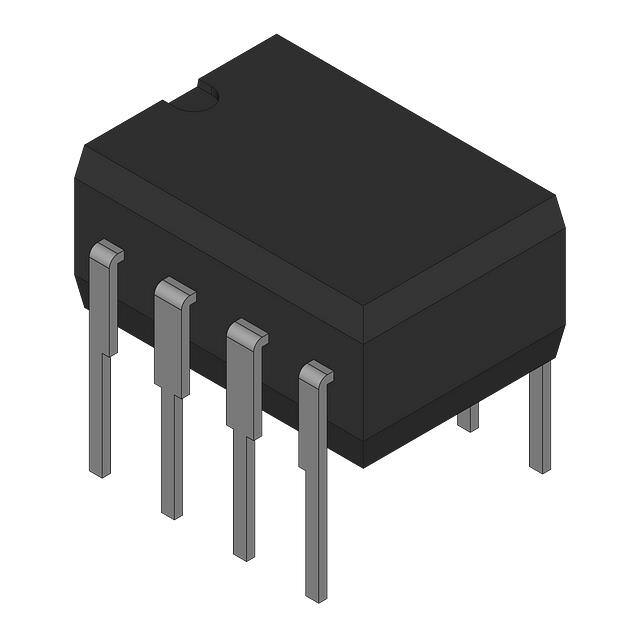
FUNCTIONAL BLOCK DIAGRAMS 8-Lead PDIP (N-8), CERDIP (Q-8) and SOIC (R-8)
NC 1 –IN 2 8 7 6 NC VOUT 1 V+ OUT NC –VS 2 +IN 3
4
5-Lead SOT-23-5 (RT-5)
AD8001
5
+VS
+IN 3 V– 4
AD8001
5
–IN
NC = NO CONNECT
transimpedance linearization circuitry. This allows it to drive video loads with excellent differential gain and phase performance on only 50 mW of power. The AD8001 is a current feedback amplifier and features gain flatness of 0.1 dB to 100 MHz while offering differential gain and phase error of 0.01% and 0.025°. This makes the AD8001 ideal for professional video electronics such as cameras and video switchers. Additionally, the AD8001’s low distortion and fast settling make it ideal for buffer high speed A-to-D converters. The AD8001 offers low power of 5.5 mA max (VS = ± 5 V) and can run on a single +12 V power supply, while being capable of delivering over 70 mA of load current. These features make this amplifier ideal for portable and battery-powered applications where size and power are critical. The outstanding bandwidth of 800 MHz along with 1200 V/µs of slew rate make the AD8001 useful in many general-purpose high speed applications where dual power supplies of up to ± 6 V and single supplies from 6 V to 12 V are needed. The AD8001 is available in the industrial temperature range of –40°C to +85°C.
The AD8001 is a low power, high speed amplifier designed to operate on ± 5 V supplies. The AD8001 features unique
9 6 3 G = +2 RL = 100 VS = 5V RFB = 820
GAIN – dB
0 –3 VS = 5V RFB = 1k
–6 –9 –12 10M
100M FREQUENCY – Hz
1G
Figure 1. Frequency Response of AD8001
Figure 2. Transient Response of AD8001; 2 V Step, G = +2
REV. D
Information furnished by Analog Devices is believed to be accurate and reliable. However, no responsibility is assumed by Analog Devices for its use, nor for any infringements of patents or other rights of third parties that may result from its use. No license is granted by implication or otherwise under any patent or patent rights of Analog Devices. Trademarks and registered trademarks are the property of their respective companies.
One Technology Way, P.O. Box 9106, Norwood, MA 02062-9106, U.S.A. Tel: 781/329-4700 www.analog.com Fax: 781/326-8703 © 2003 Analog Devices, Inc. All rights reserved.
�AD8001–SPECIFICATIONS (@ T = + 25 C, V =
A S
5 V, RL = 100
, unless otherwise noted.)
Min
350 650 350 575 300 575 85 100 120 800 960
Model
DYNAMIC PERFORMANCE –3 dB Small Signal Bandwidth, N Package R Package RT Package Bandwidth for 0.1 dB Flatness N Package R Package RT Package Slew Rate Settling Time to 0.1% Rise and Fall Time NOISE/HARMONIC PERFORMANCE Total Harmonic Distortion Input Voltage Noise Input Current Noise Differential Gain Error Differential Phase Error Third Order Intercept 1 dB Gain Compression SFDR DC PERFORMANCE Input Offset Voltage
Conditions
G = +2, < 0.1 dB Peaking, R F = 750 Ω G = +1, < 1 dB Peaking, RF = 1 kΩ G = +2, < 0.1 dB Peaking, R F = 681 Ω G = +1, < 0.1 dB Peaking, R F = 845 Ω G = +2, < 0.1 dB Peaking, R F = 768 Ω G = +1, < 0.1 dB Peaking, RF = 1 kΩ G = +2, R F = 750 Ω G = +2, R F = 681 Ω G = +2, R F = 768 Ω G = +2, VO = 2 V Step G = –1, VO = 2 V Step G = –1, VO = 2 V Step G = +2, VO = 2 V Step, RF = 649 Ω fC = 5 MHz, VO = 2 V p-p G = +2, RL = 100 Ω f = 10 kHz f = 10 kHz, +In –In NTSC, G = +2, R L = 150 Ω NTSC, G = +2, R L = 150 Ω f = 10 MHz f = 10 MHz f = 5 MHz
AD8001A Typ Max
440 880 440 715 380 795 110 125 145 1000 1200 10 1.4 –65 2.0 2.0 18 0.01 0.025 33 14 –66 2.0 2.0 10 5.0 3.0
Unit
MHz MHz MHz MHz MHz MHz MHz MHz MHz V/µs V/µs ns ns dBc nV/√Hz pA/√Hz pA/√Hz % Degree dBm dBm dB mV mV µV/°C ±µ A ±µ A ±µ A ±µ A kΩ kΩ MΩ Ω pF ±V
0.025 0.04
TMIN –TMAX Offset Drift –Input Bias Current TMIN –TMAX +Input Bias Current Open-Loop Transresistance INPUT CHARACTERISTICS Input Resistance Input Capacitance Input Common-Mode Voltage Range Common-Mode Rejection Ratio Offset Voltage –Input Current +Input Current OUTPUT CHARACTERISTICS Output Voltage Swing Output Current Short Circuit Current POWER SUPPLY Operating Range Quiescent Current Power Supply Rejection Ratio –Input Current +Input Current
Specifications subject to change without notice.
5.5 9.0 25 35 6.0 10
TMIN –TMAX VO = ± 2.5 V TMIN –TMAX +Input –Input +Input VCM = ± 2.5 V VCM = ± 2.5 V, TMIN –TMAX VCM = ± 2.5 V, TMIN –TMAX R L = 150 Ω R L = 37.5 Ω
250 175
900
10 50 1.5 3.2 50 54 0.3 0.2 3.1 70 110 ± 6.0 5.5
1.0 0.7
dB µA/V µA/V ±V mA mA V mA dB dB µA/V µA/V
2.7 50 85 ± 3.0
TMIN –TMAX +VS = +4 V to +6 V, –VS = –5 V –VS = – 4 V to – 6 V, +VS = +5 V TMIN –TMAX TMIN –TMAX
60 50
5.0 75 56 0.5 0.1
2.5 0.5
–2–
REV. D
�AD8001
ABSOLUTE MAXIMUM RATINGS 1 MAXIMUM POWER DISSIPATION
Supply Voltage . . . . . . . . . . . . . . . . . . . . . . . . . . . . . . . . 12.6 V Internal Power Dissipation @ 25°C2 PDIP Package (N) . . . . . . . . . . . . . . . . . . . . . . . . . . . . 1.3 W SOIC (R) . . . . . . . . . . . . . . . . . . . . . . . . . . . . . . . . . . . 0.8 W 8-Lead CERDIP . . . . . . . . . . . . . . . . . . . . . . . . . . . . . 1.1 W SOT-23-5 Package (RT) . . . . . . . . . . . . . . . . . . . . . . . 0.5 W Input Voltage (Common Mode) . . . . . . . . . . . . . . . . . . . . ± VS Differential Input Voltage . . . . . . . . . . . . . . . . . . . . . . . ± 1.2 V Output Short Circuit Duration . . . . . . . . . . . . . . . . . . . . . . Observe Power Derating Curves Storage Temperature Range N, R . . . . . . . . . –65°C to +125°C Operating Temperature Range (A Grade) . . . –40°C to +85°C Lead Temperature Range (Soldering 10 sec) . . . . . . . . . 300°C
NOTES 1 Stresses above those listed under Absolute Maximum Ratings may cause permanent damage to the device. This is a stress rating only; functional operation of the device at these or any other conditions above those indicated in the operational section of this specification is not implied. Exposure to absolute maximum rating conditions for extended periods may affect device reliability. 2 Specification is for device in free air: 8-Lead PDIP Package: θJA = 90°C/W 8-Lead SOIC Package: θJA = 155°C/W 8-Lead CERDIP Package: θJA = 110°C/W 5-Lead SOT-23-5 Package: θJA = 260°C/W
The maximum power that can be safely dissipated by the AD8001 is limited by the associated rise in junction temperature. The maximum safe junction temperature for plastic encapsulated devices is determined by the glass transition temperature of the plastic, approximately 150°C. Exceeding this limit temporarily may cause a shift in parametric performance due to a change in the stresses exerted on the die by the package. Exceeding a junction temperature of 175°C for an extended period can result in device failure. While the AD8001 is internally short circuit protected, this may not be sufficient to guarantee that the maximum junction temperature (150°C) is not exceeded under all conditions. To ensure proper operation, it is necessary to observe the maximum power derating curves.
2.0 8-LEAD PDIP PACKAGE 1.5 8-LEAD SOIC PACKAGE TJ = +150 C
MAXIMUM POWER DISSIPATION – W
8-LEAD CERDIP PACKAGE
1.0
0.5 5-LEAD SOT-23-5 PACKAGE 0 –50 –40 –30 –20 –10 0 10 20 30 40 50 60 AMBIENT TEMPERATURE – C
70
80
90
Figure 3. Plot of Maximum Power Dissipation vs. Temperature
ORDERING GUIDE
Model AD8001AN AD8001AQ AD8001AR AD8001AR-REEL AD8001AR-REEL7 AD8001ART-REEL AD8001ART-REEL7 AD8001ACHIPS 5962-9459301MPA*
*
Temperature Range –40°C to +85°C –55°C to +125°C –40°C to +85°C –40°C to +85°C –40°C to +85°C –40°C to +85°C –40°C to +85°C –40°C to +85°C –55°C to +125°C
Package Description 8-Lead PDIP 8-Lead CERDIP 8-Lead SOIC 13" Tape and REEL 7" Tape and REEL 13" Tape and REEL 7" Tape and REEL Die Form 8-Lead CERDIP
Package Option N-8 Q-8 R-8 R-8 R-8 RT-5 RT-5 Q-8
Branding
HEA HEA
Standard Military Drawing Device.
CAUTION ESD (electrostatic discharge) sensitive device. Electrostatic charges as high as 4000 V readily accumulate on the human body and test equipment and can discharge without detection. Although the AD8001 features proprietary ESD protection circuitry, permanent damage may occur on devices subjected to high energy electrostatic discharges. Therefore, proper ESD precautions are recommended to avoid performance degradation or loss of functionality.
WARNING!
ESD SENSITIVE DEVICE
REV. D
–3–
�AD8001–Typical Performance Characteristics
806 +VS 0.001 F 0.1 F 806 VOUT TO TEKTRONIX CSA 404 COMM. SIGNAL ANALYZER
AD8001
VIN HP8133A PULSE GENERATOR TR/TF = 50ps 50 0.1 F 0.001 F –VS RL = 100
400mV
5ns
TPC 1. Test Circuit , Gain = +2
TPC 4. 2 V Step Response, G = +2
909 +VS 0.001 F 0.1 F VOUT TO TEKTRONIX CSA 404 COMM. SIGNAL ANALYZER
AD8001
VIN LeCROY 9210 PULSE GENERATOR TR/TF = 350ps 50 0.1 F 0.001 F –VS RL = 100
TPC 2. 1 V Step Response, G = +2
TPC 5. Test Circuit, Gain = +1
0.5V
5ns
TPC 3. 2 V Step Response, G = +1
TPC 6. 100 mV Step Response, G = +1
–4–
REV. D
�AD8001
9 6 3 G = +2 RL = 100 VS = 5V RFB = 820
1000
800
–3dB BANDWIDTH – MHz
VS = 5V RL = 100 G = +2
GAIN – dB
600
0 –3 VS = 5V RFB = 1k
N PACKAGE
400 R PACKAGE 200
–6 –9 –12 10M
100M FREQUENCY – Hz
1G
0 500
600
700
800
900
1000
VALUE OF FEEDBACK RESISTOR (RF) –
TPC 7. Frequency Response, G = +2
TPC 10. –3 dB Bandwidth vs. RF
0.1 0 –0.1 –0.2 RF = 698
RF = 649
–50 5V SUPPLIES
HARMONIC DISTORTION – dBc
–60
VOUT = 2V p-p RL = 100 G = +2
RF = 750 G = +2 RL = 100 VIN = 50mV
OUTPUT – dB
–0.3 –0.4 –0.5 –0.6 –0.7 –0.8 –0.9 1M
–70 SECOND HARMONIC –80 THIRD HARMONIC –90
10M FREQUENCY – Hz
100M
–100 10k
100k
1M FREQUENCY – Hz
10M
100M
TPC 8. 0.1 dB Flatness, R Package (for N Package Add 50 Ω to RF)
TPC 11. Distortion vs. Frequency, RL = 100 Ω
DIFF PHASE – Degrees
–50 5V SUPPLIES VOUT = 2V p-p RL = 1k G = +2
0.08 0.06 0.04 0.02 0.00 1 BACK TERMINATED LOAD (150 ) 0.02 G = +2 RF = 806
HARMONIC DISTORTION – dBc
–60
2 BACK TERMINATED LOADS (75 )
–70 SECOND HARMONIC –80
DIFF GAIN – %
–90
THIRD HARMONIC
0.01 0.00 –0.01 –0.02 0
1 AND 2 BACK TERMINATED LOADS (150 AND 75 )
–100
–110 10k
100k
1M FREQUENCY – Hz
10M
100M
IRE
100
TPC 9. Distortion vs. Frequency, RL = 1 kΩ
TPC 12. Differential Gain and Differential Phase
REV. D
–5–
�AD8001
5 0 900 –5 –10 VIN = –26dBm RF = 909 –15 –20 –25 –30 –35 100M FREQUENCY – Hz 500 600 1000 N PACKAGE
–3dB BANDWIDTH – MHz
GAIN – dB
800 R PACKAGE 700 VIN = 50mV RL = 100 G = +1
600
1G
3G
900 700 800 1000 VALUE OF FEEDBACK RESISTOR (RF) –
1100
TPC 13. Frequency Response, G = +1
TPC 16. –3 dB Bandwidth vs. RF, G = +1
1 0 –1 RF = 649
–40 RL = 100 G = +1 VOUT = 2V p-p
–50
RF = 953
DISTORTION – dBc
–2
–60 SECOND HARMONIC –70
OUTPUT – dB
–3 –4 –5 –6 –7 G = +1 RL = 100 VIN = 50mV
–80
THIRD HARMONIC
–90
–8 –9 2M 10M 100M FREQUENCY – Hz 1G
–100 10k
100k
1M FREQUENCY – Hz
10M
100M
TPC 14. Flatness, R Package, G = +1 (for N Package Add 100 Ω to RF)
TPC 17. Distortion vs. Frequency, RL = 100 Ω
–40 G = +1 RL = 1k VOUT = 2V p-p
3 0 –3 –6
OUTPUT – dBV
THIRD HARMONIC
–50 –60 –70
DISTORTION – dBc
–9 –12 –15 –18 –21 RL = 100 G = +1
SECOND HARMONIC –80 –90 –100 –110 10k
–24 –27 1M
100k
1M FREQUENCY – Hz
10M
100M
10M FREQUENCY – Hz
100M
TPC 15. Distortion vs. Frequency, RL = 1 kΩ
TPC 18. Large Signal Frequency Response, G = +1
–6–
REV. D
�AD8001
45 40 35 30 25 20 GAIN – dB 15 10 5 0 –5 –10 –15 –20 –25 1M 10M 100M FREQUENCY – Hz 1G RL = 100 G = +10 RF = 470 G = +100
INPUT OFFSET VOLTAGE – mV
2.2 2.0 RF = 1000 1.8 1.6 DEVICE NO. 2 1.4 1.2 1.0 0.8 0.6 0.4 –60 DEVICE NO. 3 DEVICE NO. 1
–40
–20 0 20 40 60 JUNCTION TEMPERATURE – C
80
100
TPC 19. Frequency Response, G = +10, G = +100
TPC 22. Input Offset vs. Temperature
3.35 3.25 +VOUT
SUPPLY CURRENT – mA
5.8 5.6 5.4
OUTPUT SWING – Volts
3.15 3.05
RL = 150 VS = 5V
| –VOUT |
2.95 2.85 2.75 2.65 2.55 –60 +VOUT RL = 50 VS = 5V
5.2 5.0 4.8 VS = 5V
| –VOUT |
4.6 4.4 –60
–40
–20 0 20 40 60 JUNCTION TEMPERATURE – C
80
100
–40
–20
0 20 40 60 80 100 JUNCTION TEMPERATURE – C
120
140
TPC 20. Output Swing vs. Temperature
TPC 23. Supply Current vs. Temperature
5 4
125 120
SHORT CIRCUIT CURRENT – mA
INPUT BIAS CURRENT – A
3 –IN 2 1 0 –1 +IN –2 –3 –4 –60
115 110
SOURCE ISC
| SINK ISC |
105 100 95 90 85 –60
–40
–20
0
20
40
60
80
100
120
140
–40
JUNCTION TEMPERATURE – C
–20 0 20 40 60 JUNCTION TEMPERATURE – C
80
100
TPC 21. Input Bias Current vs. Temperature
TPC 24. Short Circuit Current vs. Temperature
REV. D
–7–
�AD8001
6
1k
5 TRANSRESISTANCE – k VS = 5V RL = 150 VOUT = 2.5V
100
4
10
3 –TZ
ROUT –
1
2
1
+TZ
0.1
G = +2 RF = 909
0 –60
–40
–20
0 20 40 60 80 100 JUNCTION TEMPERATURE – C
120
140
0.01 10k
100k
1M FREQUENCY – Hz
10M
100M
TPC 25. Transresistance vs. Temperature
TPC 28. Output Resistance vs. Frequency
100
100
1 0 RF = 576
NOISE VOLTAGE – nV/ √Hz
NOISE CURRENT – pA/ √Hz
INVERTING CURRENT VS =
5V
–1 –2 OUTPUT – dB –3 –4 –5 –6 –7 G = –1 RL = 100 VIN = 50mV RF = 649
10 NONINVERTING CURRENT VS = 5V
10
RF = 750
VOLTAGE NOISE VS = 1 10 100 1k FREQUENCY – Hz
5V 10k 1 100k
–8 –9 1M 10M 100M FREQUENCY – Hz 1G
TPC 26. Noise vs. Frequency
TPC 29. –3 dB Bandwidth vs. Frequency, G = –1
–48 –49 –CMRR –50
–52.5 –55.0 –57.5 –60.0 3V SPAN –PSRR
CMRR – dB
+CMRR –52 –53 2.5V SPAN –54
PSRR – dB
–51
–62.5 –65.0 –67.5 –70.0 –72.5 CURVES ARE FOR WORSTCASE CONDITION WHERE ONE SUPPLY IS VARIED WHILE THE OTHER IS HELD CONSTANT.
–55 –56 –60
+PSRR –75.0
–40 –20 0 20 40 60 80 100 JUNCTION TEMPERATURE – C 120 140
–77.5 –60
–40
–20 0 20 40 60 JUNCTION TEMPERATURE – C
80
100
TPC 27. CMRR vs. Temperature
TPC 30. PSRR vs. Temperature
–8–
REV. D
�AD8001
30 –10 VIN –20 910 150 VOUT PSRR – dB 62 –30 150 0 –10 –20 –30 –40 –50 –50 –60 300k 1M 10M FREQUENCY – Hz 100M 1G 1M 10M 100M FREQUENCY – Hz 1G –PSRR +PSRR RF = 909 G = +2 –PSRR 910 51 20 10 CURVES ARE FOR WORSTCASE CONDITION WHERE ONE SUPPLY IS VARIED WHILE THE OTHER IS HELD CONSTANT. +PSRR
CMRR – dB
–40
TPC 31. CMRR vs. Frequency
TPC 34. PSRR vs. Frequency
1 0 –1 –2 RF = 649 RF = 549
OUTPUT – dB
–3 –4 –5 –6 –7 –8 –9 1M 10M 100M FREQUENCY – Hz 1G G = –2 RL = 100 VIN = 50mVrms
RF = 750
TPC 32. –3 dB Bandwidth vs. Frequency, G = –2
TPC 35. 2 V Step Response, G = –1
100 90 80 70 60
COUNT
100 3 WAFER LOTS COUNT = 895 MEAN = 1.37 STD DEV = 1.13 MIN = –2.45 MAX = +4.69 90 80 CUMULATIVE 70
PERCENT
60 50 FREQ DIST 40 30 20 10 –5 –4 –3 –2 –1 0 1 2 3 INPUT OFFSET VOLTAGE – mV 4 5 0
50 40 30 20 10 0
TPC 33. 100 mV Step Response, G = –1
TPC 36. Input Offset Voltage Distribution
REV. D
–9–
�AD8001
THEORY OF OPERATION
A very simple analysis can put the operation of the AD8001, a current feedback amplifier, in familiar terms. Being a current feedback amplifier, the AD8001’s open-loop behavior is expressed as transimpedance, ∆VO/∆I–IN, or TZ. The open-loop transimpedance behaves just as the open-loop voltage gain of a voltage feedback amplifier, that is, it has a large dc value and decreases at roughly 6 dB/octave in frequency. Since the RIN is proportional to 1/gM, the equivalent voltage gain is just TZ × gM, where the gM in question is the transconductance of the input stage. This results in a low open-loop input impedance at the inverting input, a now familiar result. Using this amplifier as a follower with gain, Figure 4, basic analysis yields the following result. TZ (S ) VO =G× VIN TZ (S ) + G × RIN + R1 G = 1+ R1 R2 RIN = 1 / g M ≈ 50 Ω
Considering that additional poles contribute excess phase at high frequencies, there is a minimum feedback resistance below which peaking or oscillation may result. This fact is used to determine the optimum feedback resistance, R F. In practice, parasitic capacitance at Pin 2 will also add phase in the feedback loop, so picking an optimum value for R F can be difficult. Figure 6 illustrates this problem. Here the fine scale (0.1 dB/ div) flatness is plotted versus feedback resistance. These plots were taken using an evaluation card which is available to customers so that these results may readily be duplicated. Achieving and maintaining gain flatness of better than 0.1 dB at frequencies above 10 MHz requires careful consideration of several issues.
0.1 0 RF = 698 –0.1 –0.2
OUTPUT – dB
RF = 649
G = +2 –0.3 –0.4 –0.5 –0.6
RF = 750
R1 R2 RIN
VOUT
–0.7 –0.8
VIN
–0.9 1M
10M FREQUENCY – Hz
100M
Figure 4. Follower with Gain
Figure 6. 0.1 dB Flatness vs. Frequency
Choice of Feedback and Gain Resistors
Recognizing that G × RIN


 工商网监
湘ICP备2023018690号
工商网监
湘ICP备2023018690号
