Dual, 16 MHz, Rail-to-Rail FET Input Amplifier AD823
FEATURES
Single-supply operation Output swings rail-to-rail Input voltage range extends below ground Single-supply capability from 3 V to 36 V High load drive Capacitive load drive of 500 pF, G = +1 Output current of 15 mA, 0.5 V from supplies Excellent ac performance on 2.6 mA/amplifier −3 dB bandwidth of 16 MHz, G = +1 350 ns settling time to 0.01% (2 V step) Slew rate of 22 V/μs Good dc performance 800 μV maximum input offset voltage 2 μV/°C offset voltage drift 25 pA maximum input bias current Low distortion: −108 dBc worst harmonic @ 20 kHz Low noise: 16 nV/√Hz @ 10 kHz No phase inversion with inputs to the supply rails
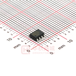
CONNECTION DIAGRAM
OUT1 1 –IN1 2 +IN1 3 –VS 4
8 7 6
+VS OUT2 +IN2
00901-001
–IN2
AD823
5
Figure 1. 8-Lead PDIP and SOIC
3V
RL = 100kΩ CL = 50pF +VS = +3V G = +1
GND 500mV 200µs
00901-002
APPLICATIONS
Battery-powered precision instrumentation Photodiode preamps Active filters 12-bit to 16-bit data acquisition systems Medical instrumentation
OUTPUT (dB)
Figure 2. Output Swing, +VS = +3 V, G = +1
2 1 0 –1 +VS = +5V G = +1
GENERAL DESCRIPTION
The AD823 is a dual precision, 16 MHz, JFET input op amp that can operate from a single supply of 3.0 V to 36 V or from dual supplies of ±1.5 V to ±18 V. It has true single-supply capability with an input voltage range extending below ground in single-supply mode. Output voltage swing extends to within 50 mV of each rail for IOUT ≤ 100 μA, providing outstanding output dynamic range. An offset voltage of 800 μV maximum, an offset voltage drift of 2 μV/°C, input bias currents below 25 pA, and low input voltage noise provide dc precision with source impedances up to a Gigaohm. It provides 16 MHz, −3 dB bandwidth, −108 dB THD @ 20 kHz, and a 22 V/μs slew rate with a low supply current of 2.6 mA per amplifier. The AD823 drives up to 500 pF of direct capacitive load as a follower and provides an output current of 15 mA, 0.5 V from the supply rails. This allows the amplifier to handle a wide range of load conditions.
–2 –3 –4 –5 –6 –7 10k 100k 1M FREQUENCY (Hz) 10M
00901-003
–8 1k
Figure 3. Small Signal Bandwidth, G = +1
This combination of ac and dc performance, plus the outstanding load drive capability, results in an exceptionally versatile amplifier for applications such as A/D drivers, high speed active filters, and other low voltage, high dynamic range systems. The AD823 is available over the industrial temperature range of −40°C to +85°C and is offered in both 8-lead PDIP and 8-lead SOIC packages.
Rev. B
Information furnished by Analog Devices is believed to be accurate and reliable. However, no responsibility is assumed by Analog Devices for its use, nor for any infringements of patents or other rights of third parties that may result from its use. Specifications subject to change without notice. No license is granted by implication or otherwise under any patent or patent rights of Analog Devices. Trademarks and registered trademarks are the property of their respective owners.
One Technology Way, P.O. Box 9106, Norwood, MA 02062-9106, U.S.A. Tel: 781.329.4700 www.analog.com Fax: 781.461.3113 ©1995–2007 Analog Devices, Inc. All rights reserved.
�AD823 TABLE OF CONTENTS
Features .............................................................................................. 1 Applications....................................................................................... 1 General Description ......................................................................... 1 Connection Diagram ....................................................................... 1 Revision History ............................................................................... 2 Specifications..................................................................................... 3 Absolute Maximum Ratings............................................................ 6 Thermal Resistance ...................................................................... 6 ESD Caution.................................................................................. 6 Typical Performance Characteristics ..............................................7 Theory of Operation ...................................................................... 13 Output Impedance ..................................................................... 14 Application Notes ........................................................................... 15 Input Characteristics.................................................................. 15 Output Characteristics............................................................... 15 Outline Dimensions ....................................................................... 18 Ordering Guide .......................................................................... 19
REVISION HISTORY
2/07—Rev. A to Rev. B Updated Format..................................................................Universal Changes to DC Performance .......................................................... 5 Updated Outline Dimensions ....................................................... 18 Changes to Ordering Guide ......................................................... 19 5/04—Rev. 0 to Rev. A Changes to Specifications ................................................................ 2 Changes to Ordering Guide ......................................................... 17 Updated Outline Dimensions ....................................................... 17 5/95—Revision 0: Initial Version
Rev. B | Page 2 of 20
�AD823 SPECIFICATIONS
At TA = 25°C, +VS = +5 V, RL = 2 kΩ to 2.5 V, unless otherwise noted. Table 1.
Parameter DYNAMIC PERFORMANCE −3 dB Bandwidth, VO ≤ 0.2 V p-p Full Power Response Slew Rate Settling Time to 0.1% to 0.01% NOISE/DISTORTION PERFORMANCE Input Voltage Noise Input Current Noise Harmonic Distortion Crosstalk f = 1 kHz f = 1 MHz DC PERFORMANCE Initial Offset Maximum Offset Over temperature Offset Drift Input Bias Current at TMAX Input Offset Current at TMAX Open-Loop Gain TMIN to TMAX INPUT CHARACTERISTICS Input Common-Mode Voltage Range Input Resistance Input Capacitance Common-Mode Rejection Ratio OUTPUT CHARACTERISTICS Output Voltage Swing IL = ±100 μA IL = ±2 mA IL = ±10 mA Output Current Short-Circuit Current Capacitive Load Drive POWER SUPPLY Operating Range Quiescent Current Power Supply Rejection Ratio Conditions G = +1 VO = 2 V p-p G = −1, VO = 4 V Step G = −1, VO = 2 V Step G = −1, VO = 2 V Step f = 10 kHz f = 1 kHz RL = 600 Ω to 2.5 V, VO = 2 V p-p, f = 20 kHz RL = 5 kΩ RL = 5 kΩ Min 12 14 Typ 16 3.5 22 320 350 16 1 −108 −105 −63 0.2 0.3 2 3 0.5 2 0.5 45 0.8 2.0 25 5 20 Max Unit MHz MHz V/μs ns ns nV/√Hz fA/√Hz dBc dB dB mV mV μV/°C pA nA pA nA V/mV V/mV V Ω pF dB
VCM = 0 V to 4 V VCM = 0 V to 4 V
VO = 0.2 V to 4 V, RL = 2 kΩ
20 20 −0.2 to +3
VCM = 0 V to 3 V
60
−0.2 to +3.8 1013 1.8 76
VOUT = 0.5 V to 4.5 V Sourcing to 2.5 V Sinking to 2.5 V G = +1 3 TMIN to TMAX, total VS = 5 V to 15 V, TMIN to TMAX 70
0.025 to 4.975 0.08 to 4.92 0.25 to 4.75 16 40 30 500 36 5.6
V V V mA mA mA pF V mA dB
5.2 80
Rev. B | Page 3 of 20
�AD823
At TA = 25°C, +VS = +3.3 V, RL = 2 kΩ to 1.65 V, unless otherwise noted. Table 2.
Parameter DYNAMIC PERFORMANCE −3 dB Bandwidth, VO ≤ 0.2 V p-p Full Power Response Slew Rate Settling Time to 0.1% to 0.01% NOISE/DISTORTION PERFORMANCE Input Voltage Noise Input Current Noise Harmonic Distortion Crosstalk f = 1 kHz f = 1 MHz DC PERFORMANCE Initial Offset Maximum Offset Over temperature Offset Drift Input Bias Current at TMAX Input Offset Current at TMAX Open-Loop Gain TMIN to TMAX INPUT CHARACTERISTICS Input Common-Mode Voltage Range Input Resistance Input Capacitance Common-Mode Rejection Ratio OUTPUT CHARACTERISTICS Output Voltage Swing IL = ±100 μA IL = ±2 mA IL = ±10 mA Output Current Short-Circuit Current Capacitive Load Drive POWER SUPPLY Operating Range Quiescent Current Power Supply Rejection Ratio Conditions G = +1 VO = 2 V p-p G = −1, VO = 2 V Step G = −1, VO = 2 V Step G = −1, VO = 2 V Step f = 10 kHz f = 1 kHz RL = 100 Ω, VO = 2 V p-p, f = 20 kHz RL = 5 kΩ RL = 5 kΩ Min 12 13 Typ 15 3.2 20 250 300 16 1 −93 −105 −63 0.2 0.5 2 3 0.5 2 0.5 30 1.5 2.5 25 5 20 Max Unit MHz MHz V/μs ns ns nV/√Hz fA/√Hz dBc dB dB mV mV μV/°C pA nA pA nA V/mV V/mV V Ω pF dB
VCM = 0 V to 2 V VCM = 0 V to 2 V
VO = 0.2 V to 2 V, RL = 2 kΩ
15 12 −0.2 to +1
VCM = 0 V to 1 V
54
−0.2 to +1.8 1013 1.8 70
VOUT = 0.5 V to 2.5 V Sourcing to 1.5 V Sinking to 1.5 V G = +1 3 TMIN to TMAX, total VS = 3.3 V to 15 V, TMIN to TMAX 70
0.025 to 3.275 0.08 to 3.22 0.25 to 3.05 15 40 30 500 36 5.7
V V V mA mA mA pF V mA dB
5.0 80
Rev. B | Page 4 of 20
�AD823
At TA = 25°C, VS = ±15 V, RL = 2 kΩ to 0 V, unless otherwise noted. Table 3.
Parameter DYNAMIC PERFORMANCE −3 dB Bandwidth, VO ≤ 0.2 V p-p Full Power Response Slew Rate Settling Time to 0.1% to 0.01% NOISE/DISTORTION PERFORMANCE Input Voltage Noise Input Current Noise Harmonic Distortion Crosstalk f = 1 kHz f = 1 MHz DC PERFORMANCE Initial Offset Maximum Offset Over temperature Offset Drift Input Bias Current at TMAX Input Offset Current at TMAX Open-Loop Gain TMIN to TMAX INPUT CHARACTERISTICS Input Common-Mode Voltage Range Input Resistance Input Capacitance Common-Mode Rejection Ratio OUTPUT CHARACTERISTICS Output Voltage Swing IL = ±100 μA IL = ±2 mA IL = ±10 mA Output Current Short-Circuit Current Capacitive Load Drive POWER SUPPLY Operating Range Quiescent Current Power Supply Rejection Ratio Conditions G = +1 VO = 2 V p-p G = −1, VO = 10 V Step G = −1, VO = 10 V Step G = −1, VO = 10 V Step f = 10 kHz f = 1 kHz RL = 600 Ω, VO = 10 V p-p, f = 20 kHz RL= 5 kΩ RL= 5 kΩ Min 12 17 Typ 16 4 25 550 650 16 1 −90 −105 −63 0.7 1.0 2 5 60 0.5 2 0.5 60 3.5 7 30 5 20 Max Unit MHz MHz V/μs ns ns nV/√Hz fA/√Hz dBc dB dB mV mV μV/°C pA pA nA pA nA V/mV V/mV V Ω pF dB
VCM = 0 V VCM = −10 V VCM = 0 V
VO = +10 V to −10 V, RL = 2 kΩ
30 30 −15.2 to +13
VCM = −15 V to +13 V
66
−15.2 to +13.8 1013 1.8 82
VOUT = −14.5 V to +14.5 V Sourcing to 0 V Sinking to 0 V G = +1 3 TMIN to TMAX, total VS = 5 V to 15 V, TMIN to TMAX 70
−14.95 to +14.95 −14.92 to +14.92 −14.75 to +14.75 17 80 60 500 36 8.4
V V V mA mA mA pF V mA dB
7.0 80
Rev. B | Page 5 of 20
�AD823 ABSOLUTE MAXIMUM RATINGS
Table 4
Parameter Supply Voltage Internal Power Dissipation PDIP (N) SOIC (R) Input Voltage (Common Mode) Differential Input Voltage Output Short-Circuit Duration Storage Temperature Range N, R Operating Temperature Range Lead Temperature Range (Soldering, 10 sec)
MAXIMUM POWER DISSIPATION (W)
Rating 36 V 1.3 W 0.9 W ±VS ±1.2 V See Figure 4 −65°C to +125°C −40°C to +85°C 300°C
2.0 8-LEAD PDIP
TJ = 150°C
1.5
1.0
8-LEAD SOIC 0.5
Stresses above those listed under Absolute Maximum Ratings may cause permanent damage to the device. This is a stress rating only; functional operation of the device at these or any other conditions above those indicated in the operational section of this specification is not implied. Exposure to absolute maximum rating conditions for extended periods may affect device reliability.
70
80 90
Figure 4. Maximum Power Dissipation vs. Temperature
THERMAL RESISTANCE
θJA is specified for the worst-case conditions, that is, a device soldered in a circuit board for surface-mount packages. Specification is for device in free air. Table 5. Thermal Resistance
Package Type 8-Lead PDIP 8-Lead SOIC θJA 90 160 Unit °C/W °C/W
ESD CAUTION
Rev. B | Page 6 of 20
00901-004
0 –50 –40 –30 –20 –10 0 10 20 30 40 50 60 AMBIENT TEMPERATURE (°C)
�AD823 TYPICAL PERFORMANCE CHARACTERISTICS
80 70 60 50
UNITS
+VS = +5V 314 UNITS σ = 40µV
100 90 80 70 60
UNITS
+VS = +5V 317 UNITS σ = 0.4pA
40 30 20 10
00901-005
50 40 30 20 10
–150
–100 –50 0 50 100 INPUT OFFSET VOLTAGE (µV)
150
200
0
1
2
3 4 5 6 7 INPUT BIAS CURRENT (pA)
8
9
10
Figure 5. Typical Distribution of Input Offset Voltage
Figure 8. Typical Distribution of Input Bias Current
22 20 18 16 14
UNITS
+VS = +5V –55°C TO +125°C 103 UNITS
10000
+VS = +5V VCM = 0V
INPUT BIAS CURRENT (pA)
1000
100
12 10 8 6 4 2
00901-006
10
1
–5
–4
–3 –2 –1 0 3 4 5 1 2 INPUT OFFSET VOLTAGE DRIFT (µV/°C)
6
7
25
50 75 TEMPERATURE (°C)
100
125
Figure 6. Typical Distribution of Input Offset Voltage Drift
Figure 9. Input Bias Current vs. Temperature
3 2
+VS = +5V
1000
VS = ±15V
INPUT BIAS CURRENT (pA)
INPUT BIAS CURRENT (pA)
1 0 –1 –2 –3 –4 –5
100
10
1
00901-007
–4
–3
–2 –1 0 1 2 3 COMMON-MODE VOLTAGE (V)
4
5
–12
–8 –4 0 4 8 COMMON-MODE VOLTAGE (V)
12
16
Figure 7. Input Bias Current vs. Common-Mode Voltage
Figure 10. Input Bias Current vs. Common-Mode Voltage
Rev. B | Page 7 of 20
00901-010
0.1 –16
00901-009
0 –6
0.1 0
00901-008
0 –200
0
�AD823
110 VS = ±2.5V 95 94 100 93 RL = 2kΩ +VS = +5V
OPEN-LOOP GAIN (dB)
OPEN-LOOP GAIN (dB)
00901-011
92 91 90 89 88 87
90
80
70
1k
10k LOAD RESISTANCE (Ω)
100k
500k
–25
5 35 65 TEMPERATURE (°C)
95
125
Figure 11. Open-Loop Gain vs. Load Resistance
1000 RL = 10kΩ
OPEN-LOOP GAIN (k V ) V
Figure 14. Open-Loop Gain vs. Temperature
100 100
RL = 2kΩ CL = 20pF
100
OPEN-LOOP GAIN (dB)
RL = 1kΩ 10 RL = 100Ω 1
60
PHASE
60
40 GAIN 20
40
20
0
00901-012
0
1k
10k
100k
1M
10M
FREQUENCY (Hz)
Figure 12. Open-Loop Gain vs. Output Voltage, VS = ±2.5 V
–40 –50 –60
THD (dB)
Figure 15. Open-Loop Gain and Phase Margin vs. Frequency
100
+VS = +5V
–70 –80 –90 –100 –110 100
+VS = +3V VOUT = 2V p-p RL = 100Ω VS = ±2.5V VOUT = 2V p-p VS = ±15V RL = 1kΩ VOUT = 10V p-p RL = 600Ω
INPUT VOLTAGE NOISE (nV/√Hz)
30
ALL OTHERS
+VS = +3V VOUT = 2V p-p RL = 5kΩ +VS = +5V VOUT = 2V p-p RL = 5kΩ
00901-013
10
1k
10k FREQUENCY (Hz)
100k
1M
10
100
1k 10k FREQUENCY (Hz)
100k
1M
Figure 13. Total Harmonic Distortion vs. Frequency
Figure 16. Input Voltage Noise vs. Frequency
Rev. B | Page 8 of 20
00901-016
3
00901-015
0.1 0.5 1.0 –2.5 –2.0 –1.5 –1.0 –0.5 0 OUTPUT VOLTAGE (V)
1.5
2.0
2.5
–20 100
–20 100M
PHASE MARGIN (Degrees)
80
80
00901-014
60 100
86 –55
�AD823
5 4 CL = 20pF RL = 2kΩ G = +1
90 80 70
CMRR (dB)
VS = ±15V +VS = +5V
CLOSED-LOOP GAIN (dB)
3 2 1 0 –1 –2 –3 –4
00901-017
60 50 40 30 20 10
+27°C +125°C
–55°C
100
1k
10k 100k FREQUENCY (Hz)
1M
10M
Figure 17. Closed-Loop Gain vs. Frequency
100
Figure 20. Common-Mode Rejection Ratio vs. Frequency
10
+VS = +5V GAIN = +1
+VS = +5V
10
OUTPUT SATURATION VOLTAGE (V)
OUTPUT RESISTANCE ( Ω)
1 VS – VOH 25°C
1
0.1
0.1
VOL 25°C
00901-018
1k
10k 100k FREQUENCY (Hz)
1M
10M
1 10 LOAD CURRENT (mA)
100
Figure 18. Output Resistance vs. Frequency, +VS = +5 V, Gain = +1
10 8 6 4 2 0 –2 –4 –6 –8
00901-019
Figure 21. Output Saturation Voltage vs. Load Current
10
OUTPUT STEP SIZE FROM 0V TO VSHOWN (V)
VS = ±15V CL = 20pF
1%
0.1%
0.01%
QUIESCENT CURRENT (mA)
8
+125°C +25°C
6
–55°C
4
1%
0.1%
0.01%
2
200
300
400
500
600
700
0
5
SETTLING TIME (ns)
10 15 SUPPLY VOLTAGE (±V)
20
Figure 19. Output Step Size vs. Settling Time (Inverter)
Figure 22. Quiescent Current vs. Supply Voltage
Rev. B | Page 9 of 20
00901-022
–10 100
0
00901-021
0.01 100
0.01 0.1
00901-020
–5 0.30 3.27 6.24 9.21 12.18 15.15 18.12 21.09 24.06 27.03 30.00 FREQUENCY (MHz)
�AD823
100 90 +VS = +5V
21 18
SERIES RESISTANCE ( Ω)
+VS = +5V VIN
RS CL
POWER SUPPLY REJECTION (dB)
80 70 60 50 40 30 20 10
00901-023
15 12 9 ФM = 45° 6 ФM = 20° 3
00901-026
+PSRR
–PSRR
0 100
1k
10k 100k FREQUENCY (Hz)
1M
10M
0
0
1
2
3 4 5 6 7 CAPACITOR (pF × 1000)
8
9
10
Figure 23. Power Supply Rejection vs. Frequency
30
Figure 26. Series Resistance vs. Capacitive Load
–30 –40 –50
CROSSTALK (dB)
RL = 2kΩ G = +1
+VS = +5V
OUTPUT VOLTAGE (V p-p)
20 VS = ±15V
–60 –70 –80 –90 –100 –110 –120
10 +VS = +5V +VS = +3V
00901-024
100k 1M FREQUENCY (Hz)
10M
10k
100k FREQUENCY (Hz)
1M
10M
Figure 24. Large Signal Frequency Response
VIN = 2.9V p-p +VS = +3V G = –1
Figure 27. Crosstalk vs. Frequency
VIN = 20V p-p VS = ±15V G = +1
500mV 100k Ω 100k Ω VIN = 2.9V p-p 50Ω 100k Ω 3V
10µs
5V +15V
20µs
VOUT
00901-025
20kHz, 20V p-p
00901-028
50pF
–15V
604Ω
50pF
Figure 25. Output Swing, +VS = +3 V, G = −1
Figure 28. Output Swing, VS = ±15 V, G = +1
Rev. B | Page 10 of 20
00901-027
0 10k
–130 1k
�AD823
5V RL = 300Ω CL = 50pF RF = RG = 2kΩ +VS = +5V G = –1
RL = 100kΩ CL = 50pF +VS = +3V G = +1
3V
GND
00901-029
500mV GND
200µs
500mV
200µs
Figure 29. Output Swing, +VS = +5 V, G = −1
Figure 32. Output Swing, +VS = +3 V, G = +1
VIN = 100mV STEP +VS = +3V G = +1
5V
RL = 2kΩ CL = 50pF +VS = +5V G = +1
1.55V
1.45V
00901-030
25mV
50ns
500mV GND
100ns
Figure 30. Pulse Response, +VS = +3 V, G = +1
Figure 33. Pulse Response, +VS = +5 V, G = +1
5V
RL = 2kΩ CL = 50pF +VS = +5V G = +2
RL = 2kΩ CL = 470pF +VS = +5V G = +1
00901-031
500mV GND
100ns
500mV
200ns
Figure 31. Pulse Response, +VS = +5 V, G = +2
Figure 34. Pulse Response, +VS = +5 V, G = +1, CL = 470 pF
Rev. B | Page 11 of 20
00901-034
00901-033
00901-032
�AD823
RL = 100kΩ CL = 50pF VS = ±15V G = +1 +10V
–10V
5V
500ns
Figure 35. Pulse Response, VS = ±15 V, G = +1
00901-035
Rev. B | Page 12 of 20
�AD823 THEORY OF OPERATION
The AD823 is fabricated on the Analog Devices, Inc. proprietary complementary bipolar (CB) process that enables the construction of PNP and NPN transistors with similar fT’s in the 600 MHz to 800 MHz region. In addition, the process also features N-Channel JFETs that are used in the input stage of the AD823. These process features allow the construction of high frequency, low distortion op amps with picoamp input currents. This design uses a differential output input stage to maximize bandwidth and headroom (see Figure 36). The smaller signal swings required on the S1P/S1N outputs reduce the effect of the nonlinear currents due to junction capacitances and improve the distortion performance. With this design, harmonic distortion of better than −91 dB @ 20 kHz into 600 Ω with VOUT = 4 V p-p on a single 5 V supply is achieved. The complementary common emitter design of the output stage provides excellent load drive without the need for emitter followers, thereby improving the output range of the device considerably with respect to conventional op amps. The AD823 can drive 20 mA with the outputs within 0.6 V of the supply rails. The AD823 also offers outstanding precision for a high speed op amp. Input offset voltages of 1 mV maximum and offset drift of 2 μV/°C are achieved through the use of the Analog Devices advanced thin film trimming techniques.
VCC R42 R37 VBE + 0.3V V1 I5 Q43 Q55 I6
A nested integrator topology is used in the AD823 (see Figure 37). The output stage can be modeled as an ideal op amp with a single-pole response and a unity-gain frequency set by transconductance gm2 and Capacitor C2. R1 is the output impedance of the input stage; gm is the input transconductance. C1 and C5 provide Miller compensation for the overall op amp. The unity-gain frequency occurs at gm/C5. Solving the node equations for this circuit yields
V OUT Vi
where:
=
A0
(sR1[C1( A2 + 1)] + 1) × ⎛ s ⎡ ⎜⎢ ⎜
g m2 ⎤ ⎞ + 1⎟ ⎟ ⎣ C2 ⎥ ⎠ ⎦ ⎝
A0 = gmgm2 R2R1 (open-loop gain of op amp) A2 = gm2 R2 (open-loop gain of output stage). The first pole in the denominator is the dominant pole of the amplifier and occurs at ~18 Hz. This equals the input stage output impedance R1 multiplied by the Miller-multiplied value of C1. The second pole occurs at the unity-gain bandwidth of the output stage, which is 23 MHz. This type of architecture allows more open-loop gain and output drive to be obtained than a standard 2-stage architecture would allow.
Q44 A=1 Q57 A = 19
Q72 VINP J1 J6
Q61 Q46
Q58
Q49 Q18 C2
R44 Q21
R28 Q54 VOUT
VINN
S1P
S1N
Q62
Q60 C1 VB
VCC Q48 Q53 Q35
I1
C6
R33
I2
R43 I3 Q56 Q52 I4
Q17 A = 19 Q59 A=1
VEE
Figure 36. Simplified Schematic
Rev. B | Page 13 of 20
00901-036
�AD823
OUTPUT IMPEDANCE
The low frequency open-loop output impedance of the commonemitter output stage used in this design is approximately 30 kΩ. Although this is significantly higher than a typical emitter follower output stage, when it is connected with feedback, the output impedance is reduced by the open-loop gain of the op amp. With 109 dB of open-loop gain, the output impedance is reduced to