Low Cost, Zero-Drift In-Amp
with Filter and Fixed Gain
AD8293G80/AD8293G160
FEATURES
FUNCTIONAL BLOCK DIAGRAM
7
5
+VS
6
FILT
R2
+IN
8
OUT
R1
4kΩ
R3
5kΩ
IN-AMP
ADC OUT
4
–IN
1
AD8293Gxx
GND REF
2
OUTPUT TO ADC
WITH ANTIALIASING
FILTER
07451-001
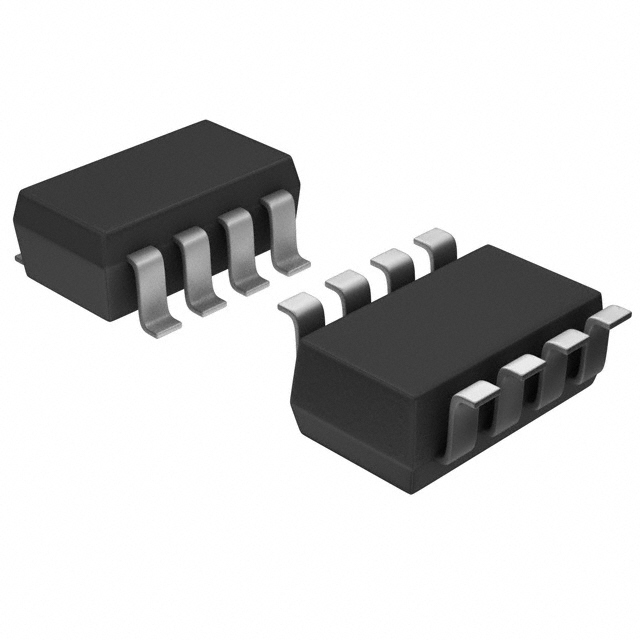
Small package: 8-lead SOT-23
Reduced component count
Incorporates gain resistors and filter resistors
Low offset voltage: 20 μV maximum
Low offset drift: 0.3 μV/°C maximum
Low gain drift: 25 ppm/°C maximum
High CMR: 140 dB typical
Low noise: 0.7 μV p-p from 0.01 Hz to 10 Hz
Single-supply operation: 1.8 V to 5.5 V
Rail-to-rail output
Available in 2 fixed-gain models
3
Figure 1.
+5V
Current sensing
Strain gauges
Laser diode control loops
Portable medical instruments
Thermocouple amplifiers
C2
0.1µF
7
6
5
+VS
FILT
LOAD
8
I
+IN
R1
4kΩ
RSHUNT
1
OUT
R2
IN-AMP
R3
5kΩ
ADC OUT
C3
+3.3V
1.8V
DC-DC
ADC
4
–IN
AD8293Gxx
GND REF
2
REF
0.1µF
10µF
3
07451-002
APPLICATIONS
Figure 2. Measuring Current Using the AD8293G80/AD8293G160
Table 1. AD8293Gxx Models and Gains
Model
AD8293G80
AD8293G160
Gain
80
160
GENERAL DESCRIPTION
The AD8293G80/AD8293G160 are small, low cost, precision
instrumentation amplifiers that have low noise and rail-to-rail
outputs. They are available in two fixed-gain models: 80 and 160.
They incorporate the gain setting resistors and filter resistors,
reducing the number of ancillary components. For example,
only two external capacitors are needed to implement a 2-pole
filter. The AD8293G80/AD8293G160 also feature low offset
voltage, offset drift, and gain drift coupled with high commonmode rejection. They are capable of operating on a supply of
1.8 V to 5.5 V.
With a low offset voltage of 20 μV (AD8293G160B), an offset
voltage drift of 0.3 μV/°C, and a voltage noise of only 0.7 μV p-p
(0.01 Hz to 10 Hz), the AD8293G80/AD8293G160 are ideal
for applications where error sources cannot be tolerated.
Precision instrumentation, position and pressure sensors,
medical instrumentation, and strain gauge amplifiers benefit
from the low noise, low input bias current, and high commonmode rejection. The small footprint and low cost are ideal for
high volume applications.
The small package and low power consumption allow the maximum channel density and the minimum board size required for
portable systems. Designed for ease of use, these instrumentation
amplifiers, unlike more traditional ones, have a buffered reference,
eliminating the need for an additional op amp to set the reference
voltage to midsupply.
The AD8293G80/AD8293G160 are specified over the industrial
temperature range from −40°C to +85°C. The AD8293G80/
AD8293G160 are available in a halogen-free, Pb-free, 8-lead SOT-23.
Rev. 0
Information furnished by Analog Devices is believed to be accurate and reliable. However, no
responsibility is assumed by Analog Devices for its use, nor for any infringements of patents or other
rights of third parties that may result from its use. Specifications subject to change without notice. No
license is granted by implication or otherwise under any patent or patent rights of Analog Devices.
Trademarks and registered trademarks are the property of their respective owners.
One Technology Way, P.O. Box 9106, Norwood, MA 02062-9106, U.S.A.
Tel: 781.329.4700
www.analog.com
Fax: 781.461.3113
©2008 Analog Devices, Inc. All rights reserved.
�AD8293G80/AD8293G160
TABLE OF CONTENTS
Features .............................................................................................. 1
Theory of Operation ...................................................................... 10
Applications ....................................................................................... 1
High PSR and CMR ................................................................... 10
Functional Block Diagram .............................................................. 1
1/f Noise Correction .................................................................. 10
General Description ......................................................................... 1
Applications Information .............................................................. 11
Revision History ............................................................................... 2
Overview ..................................................................................... 11
Specifications..................................................................................... 3
Reference Connection ............................................................... 11
Electrical Characteristics ............................................................. 3
Output Filtering .......................................................................... 11
Absolute Maximum Ratings............................................................ 5
Clock Feedthrough..................................................................... 12
Thermal Resistance ...................................................................... 5
Power Supply Bypassing ............................................................ 12
ESD Caution .................................................................................. 5
Input Overvoltage Protection ................................................... 12
Pin Configuration and Function Descriptions ............................. 6
Outline Dimensions ....................................................................... 13
Typical Performance Characteristics ............................................. 7
Ordering Guide .......................................................................... 13
REVISION HISTORY
8/08—Revision 0: Initial Version
Rev. 0 | Page 2 of 16
�AD8293G80/AD8293G160
SPECIFICATIONS
ELECTRICAL CHARACTERISTICS
VCC = 5.0 V, VCM = −0 V, VREF = 3.3 V, VIN = VINP − VINN, TA = 25°C, tested at ADC OUT, unless otherwise noted. Temperature
specifications guaranteed by characterization.
Table 2. A Grade
Parameter
COMMON-MODE REJECTION
NOISE PERFORMANCE
Voltage Noise
Voltage Noise Density
INPUT CHARACTERISTICS
Input Offset Voltage
vs. Temperature
Input Bias Current
Input Offset Current
Input Operating Impedance
Differential
Common Mode
Input Voltage Range
DYNAMIC RESPONSE
Small Signal Bandwidth 1
Slew Rate
Settling Time 2
0.1%
0.01%
Internal Clock Frequency
GAIN
Gain Error
Gain Drift
Nonlinearity
OUTPUT CHARACTERISTICS
Output Voltage High
Output Voltage Low
Short-Circuit Current
REFERENCE CHARACTERISTICS
VREF Range
REF Pin Current
POWER SUPPLY
Operating Range
Power Supply Rejection
Supply Current
Conditions
VCM = 0 V to 3.3 V,
−40°C ≤ TA ≤ +85°C
en p-p
en
f = 0.01 Hz to 10 Hz
f = 1 kHz
0.7
35
VOS
ΔVOS/ΔT
IB
IOS
−40°C ≤ TA ≤ +85°C
−40°C ≤ TA ≤ +85°C
9
0.02
0.4
2
Min
94
0
BW
SR
ts
Filter limited
50
0.3
2
4
9
0.02
0.4
VCC − 1.7
1.9
2.4
60
80
0.3
5
0.003
VO = 0.075 V to 4.925 V
−40°C ≤ TA ≤ +85°C
VO = 0.075 V to 4.925 V
VOH
1.9
2.4
60
160
0.3
5
0.003
0.8
0.01
1.8
94
−40
Higher bandwidths result in higher noise.
Settling time is determined by filter setting.
Rev. 0 | Page 3 of 16
VCC − 1.7
MΩ||pF
GΩ||pF
V
ms
ms
kHz
1
25
0.03
120
1.0
0.8
5.5
1.8
94
0.01
1.3
1.5
+85
−40
%
ppm/°C
% FS
0.075
V
mA
VCC − 0.8
1
V
nA
5.5
1.3
1.5
V
dB
mA
mA
+85
°C
±35
VCC − 0.8
1
Hz
V
0.075
VCC = 1.8 V to 5.5 V, VCM = 0 V
IO = 0 mA, VIN = 0 V
−40°C ≤ TA ≤ +85°C
μV
μV/°C
nA
nA
VCC −
0.075
±35
IREF
50
0.3
2
4
500
Filter limited
1
25
0.03
VCC −
0.075
VOL
ISC
PSR
ISY
0
Unit
dB
μV p-p
nV/√Hz
50||1
10||10
500
Filter limited
500 Hz filter, VO = 2 V step
AD8293G160A
Typ
Max
140
0.7
35
50||1
10||10
TEMPERATURE RANGE
Specified Range
1
Min
94
AD8293G80A
Typ
Max
140
Symbol
CMR
120
1.0
�AD8293G80/AD8293G160
VCC = 2.7 V to 5.0 V, VCM = −0 V, VREF = VCC/2, VIN = VINP − VINN, TA = 25°C, tested at OUT with 10 kΩ load and ADC OUT, unless
otherwise noted. Temperature specifications guaranteed by characterization.
Table 3. B Grade (Tested and Guaranteed over a Wider Supply Range to More Stringent Specifications Than the A Grade)
Parameter
COMMON-MODE REJECTION
NOISE PERFORMANCE
Voltage Noise
Voltage Noise Density
INPUT CHARACTERISTICS
Input Offset Voltage
vs. Temperature
vs. Temperature
Input Bias Current
Input Offset Current
Input Operating Impedance
Differential
Common Mode
Input Voltage Range
DYNAMIC RESPONSE
Small Signal Bandwidth 1
Slew Rate
Settling Time 2
0.1%
0.01%
Internal Clock Frequency
GAIN
Gain Error
Gain Drift
Nonlinearity
OUTPUT CHARACTERISTICS
Output Voltage High
Output Voltage Low
Short-Circuit Current
REFERENCE CHARACTERISTICS
VREF Range
REF Pin Current
POWER SUPPLY
Operating Range
Power Supply Rejection
Supply Current
Symbol
CMR
2
Min
110
106
AD8293G80B
Typ
Max
140
140
en p-p
en
f = 0.01 Hz to 10 Hz
f = 1 kHz
0.7
35
VOS
ΔVOS/ΔT
ΔVOS/ΔT
IB
IOS
−40°C ≤ TA ≤ +85°C, VCC = 5 V
−40°C ≤ TA ≤ +85°C, VCC = 2.7 V
−40°C ≤ TA ≤ +85°C
5
0.02
0.01
0.4
Min
110
AD8293G160B
Typ
Max
140
106
30
0.3
0.5
2
4
0
BW
SR
ts
VO = 0.075 V to 4.925 V
−40°C ≤ TA ≤ +85°C
VO = 0.075 V to 4.925 V
VOH
VOL
ISC
2.4
60
80
0.3
5
0.003
2.4
60
160
0.3
5
0.003
ms
kHz
0.5
25
0.009
Higher bandwidths result in higher noise.
Settling time is determined by filter setting.
Rev. 0 | Page 4 of 16
0.5
25
0.009
120
1.0
0.075
V
mA
mA
VCC − 0.8
1
V
nA
5.5
1.3
1.5
V
dB
mA
mA
+85
°C
±35
±25
VCC − 0.8
1
0.8
5.5
1.8
100
0.01
1.3
1.5
+85
−40
%
ppm/°C
% FS
V
VCC −
0.075
0.01
−40
Hz
ms
0.8
1.8
100
VCC − 1.7
MΩ||pF
GΩ||pF
V
1.9
±35
±25
VCC = 1.8 V to 5.5 V, VCM = 0 V
IO = 0 mA, VIN = 0 V
−40°C ≤ TA ≤ +85°C
μV
μV/°C
μV/°C
nA
nA
Filter limited
0.075
VCC = 5 V
VCC = 2.7 V
20
0.3
0.5
2
4
1.9
VCC −
0.075
IREF
PSR
ISY
μV p-p
nV/√Hz
500
Filter limited
500 Hz filter, VO = 2 V step;
measured at ADC OUT
0.7
35
0
500
Filter limited; measured at
ADC OUT
dB
50||1
10||10
VCC − 1.7
Unit
dB
140
3
0.02
0.01
0.4
50||1
10||10
TEMPERATURE RANGE
Specified Range
1
Conditions
VCC = 5 V, VCM = 0 V to 3.3 V;
−40°C ≤ TA ≤ +85°C
VCC = 2.7 V, VCM = 0 V to 1 V;
−40°C ≤ TA ≤ +85°C
120
1.0
�AD8293G80/AD8293G160
ABSOLUTE MAXIMUM RATINGS
Table 4.
Parameter
Supply Voltage
Input Voltage
Differential Input Voltage1
Output Short-Circuit Duration to GND
Storage Temperature Range (RJ Package)
Operating Temperature Range
Junction Temperature Range (RJ Package)
Lead Temperature (Soldering, 10 sec)
1
Rating
6V
+VSUPPLY
±VSUPPLY
Indefinite
−65°C to +150°C
−40°C to +85°C
−65°C to +150°C
300°C
Differential input voltage is limited to ±5.0 V, the supply voltage, or
whichever is less.
Stresses above those listed under Absolute Maximum Ratings
may cause permanent damage to the device. This is a stress
rating only; functional operation of the device at these or any
other conditions above those indicated in the operational
section of this specification is not implied. Exposure to absolute
maximum rating conditions for extended periods may affect
device reliability.
THERMAL RESISTANCE
θJA is specified for the worst-case conditions, that is, a device
soldered in a circuit board for surface-mount packages.
Table 5.
Package Type
8-Lead SOT-23 (RJ)
1
θJA1
211.5
θJC
91.99
Unit
°C/W
θJA is specified for the nominal conditions, that is, θJA is specified for the
device soldered on a circuit board.
ESD CAUTION
Rev. 0 | Page 5 of 16
�AD8293G80/AD8293G160
AD8293Gxx
8
+IN
2
7
+VS
REF
3
6
OUT
ADC OUT
4
5
FILT
–IN
1
GND
TOP VIEW
(Not to Scale)
07451-003
PIN CONFIGURATION AND FUNCTION DESCRIPTIONS
Figure 3. Pin Configuration
Table 6. Pin Function Descriptions
Pin No.
1
2
3
4
5
6
7
8
Mnemonic
−IN
GND
REF
ADC OUT
FILT
OUT
+VS
+IN
Description
Inverting Input Terminal (True Differential Input)
Ground
Reference Voltage Terminal (Drive This Terminal to Level-Shift the Output)
Output with Series 5 kΩ Resistor for Use with an Antialiasing Filter
Place a capacitor across FILT and OUT to limit the amount of switching noise at the output (see Applications Information)
Output Terminal Without Integrated Filter
Positive Power Supply Terminal
Noninverting Input Terminal (True Differential Input)
Rev. 0 | Page 6 of 16
�AD8293G80/AD8293G160
TYPICAL PERFORMANCE CHARACTERISTICS
TA = 25°C, VCC = 5 V, and VREF = VCC/2; G = 80, C2 = 1300 pF, and C3 = 39 nF; G = 160, C2 = 680 pF, and C3 = 39 nF, unless otherwise specified.
60
60
VCC = 2.7V, 5V
FILTER = 500Hz
VCC = 2.7V, 5V
FILTER = 10kHz
G = 160
40
40
20
GAIN (dB)
GAIN (dB)
G = 160
G = 80
0
G = 80
20
0
1k
FREQUENCY (Hz)
10k
100k
–20
10
100
Figure 4. Gain vs. Frequency
120
120
CMR (dB)
140
100
100
80
80
60
60
40
40
100
1k
10k
100k
FREQUENCY (Hz)
20
10
1k
10k
100k
Figure 8. Common-Mode Rejection (CMR) vs. Frequency
4
4
(0.02V, 3V)
(4.98V, 3.3V)
INPUT COMMON-MODE VOLTAGE (V)
(0.02V, 3.3V)
VCC = 5V, VREF = VCC/2
3
2
(0.02V, 1V)
1
(2.68V, 1V)
VCC = 2.7V,
VREF = VCC/2
(2.68V, 0V)
0
(0.02V, 0V)
0
(4.98V, 0V)
1
2
3
OUTPUT VOLTAGE (V)
4
5
6
(4.98V, 3V)
3
VCC = 5V, VREF = VCC/2
2
(0.02V, 1V)
(2.68V, 1V)
1
VCC = 2.7V,
VREF = VCC/2
0
(2.68V, 0V)
(4.98V, 0V)
(0.02V, 0V)
–1
–1
07451-018
INPUT COMMON-MODE VOLTAGE (V)
100
FREQUENCY (Hz)
Figure 5. Common-Mode Rejection (CMR) vs. Frequency
–1
–1
VCC = 2.7V, 5V
GAIN = 80, 160
FILTER = 10kHz
160
07451-005
CMR (dB)
180
140
20
10
100k
Figure 7. Gain vs. Frequency
VCC = 2.7V, 5V
GAIN = 80, 160
FILTER = 500Hz
160
10k
0
1
2
3
OUTPUT VOLTAGE (V)
Figure 6. Input Common-Mode Voltage Range vs. Output Voltage, G = 80
4
5
6
07451-019
180
1k
FREQUENCY (Hz)
07451-008
100
07451-004
–40
10
07451-007
–20
Figure 9. Input Common-Mode Voltage Range vs. Output Voltage, G = 160
Rev. 0 | Page 7 of 16
�AD8293G80/AD8293G160
10
10
POWER SUPPLY ON
4μV OFFSET
0
–5
GAIN = 160
–10
GAIN = 80
–15
–20
0
0.2
0.4
0.6
0.8
1.0
1.2
07451-010
–25
–0.2
VCC = 2.7V
VCC = 5V
1.4
TIME (ms)
5
4μV OFFSET
0
–5
GAIN = 160
GAIN = 80
–10
VCC = 2.7V
VCC = 5V
–15
–0.05
0
0.05
0.10
0.15
07451-012
INPUT OFFSET VOLTAGE (5mV/DIV)
INPUT OFFSET VOLTAGE (5mV/DIV)
POWER SUPPLY ON
5
0.20
TIME (ms)
Figure 13. Input Offset Voltage vs. Turn-On Time, Filter = 10 kHz
Figure 10. Input Offset Voltage vs. Turn-On Time, Filter = 500 Hz
GAIN = 160
GAIN = 80
10
1
0.01
0.1
1
10
100
1k
10k
100k
FREQUENCY (Hz)
TIME (10s/DIV)
Figure 14. 0.01 Hz to 10 Hz Voltage Noise
Figure 11. Voltage Noise Density
0.30
160
0.25
140
07451-025
VOLTAGE NOISE (200nV/DIV)
100
07451-009
NOISE (nV/ Hz)
1000
GAIN = 160
VCC = 2.7V, 5V
G = 80, 160
0.20
120
0.15
50mV/DIV
GAIN = 80
80
0.10
0.05
0
60
–0.05
20
10
–0.10
500Hz FILTER
10kHz FILTER
100
1k
10k
FREQUENCY (Hz)
100k
500Hz FILTER
–0.15
1ms/DIV
Figure 15. Small Signal Step Response
Figure 12. Power Supply Rejection (PSR) vs. Frequency
Rev. 0 | Page 8 of 16
07451-011
40
07451-024
PSR (dB)
10kHz FILTER
100
�AD8293G80/AD8293G160
VCC = 5V
G = 80, 160
10kHz FILTER
1V/DIV
10kHz FILTER
1ms/DIV
1ms/DIV
Figure 16. Large Signal Step Response
Figure 17. Large Signal Step Response
Rev. 0 | Page 9 of 16
07451-017
500Hz FILTER
500Hz FILTER
07451-013
500mV/DIV
VCC = 2.7V
G = 80, 160
�AD8293G80/AD8293G160
THEORY OF OPERATION
The AD8293G80/AD8293G160 are precision current-mode
correction instrumentation amplifiers capable of single-supply
operation. The current-mode correction topology results in
excellent accuracy. Figure 18 shows a simplified diagram
illustrating the basic operation of the AD8293G80/AD8293G160
(without correction). The circuit consists of a voltage-to-current
amplifier (M1 to M6), followed by a current-to-voltage amplifier
(R2 and A1). Application of a differential input voltage forces a
current through External Resistor R1, resulting in conversion of
the input voltage to a signal current. Transistor M3 to Transistor
M6 transfer twice this signal current to the inverting input of
the op amp A1. Amplifier A1 and External Resistor R2 form
a current-to-voltage converter to produce a rail-to-rail output
voltage at VOUT.
HIGH PSR AND CMR
Common-mode rejection and power supply rejection indicate
the amount that the offset voltage of an amplifier changes when
its common-mode input voltage or power supply voltage changes.
The autocorrection architecture of the AD8293G80/AD8293G160
continuously corrects for offset errors, including those induced
by changes in input or supply voltage, resulting in exceptional
rejection performance. The continuous autocorrection provides
great CMR and PSR performances over the entire operating
temperature range (−40°C to +85°C).
The parasitic resistance in series with R2 does not degrade CMR,
but causes a small gain error and a very small offset error.
Therefore, an external buffer amplifier is not required to drive
VREF to maintain excellent CMR performance. This helps reduce
system costs over conventional instrumentation amplifiers.
Op amp A1 is a high precision auto-zero amplifier. This amplifier
preserves the performance of the autocorrecting, current-mode
amplifier topology while offering the user a true voltage-in,
voltage-out instrumentation amplifier. Offset errors are corrected
internally.
1/f NOISE CORRECTION
Flicker noise, also known as 1/f noise, is noise inherent in the
physics of semiconductor devices and decreases 10 dB per decade.
The 1/f corner frequency of an amplifier is the frequency at which
the flicker noise is equal to the broadband noise of the amplifier. At
lower frequencies, flicker noise dominates, causing large errors
in low frequency or dc applications.
An external reference voltage is applied to the noninverting
input of A1 to set the output reference level. External Capacitor
C2 is used to filter out correction noise.
Flicker noise is seen effectively as a slowly varying offset
error, which is reduced by the autocorrection topology of the
AD8293G80/AD8293G160. This allows the AD8293G80/
AD8293G160 to have lower noise near dc than standard low
noise instrumentation amplifiers.
VCC
C2
I
M5
M6
R1
I – IR1
IR1 =
VINP
M1
2I
R2
I – IR1
R1
VBIAS
M2
VINN
M3
M4
+
2R2
R1
VINP – VINN
2IR1
R3
I + IR1
(VINP – VINN)
VOUT = VREF
A1
VREF
2I
EXTERNAL
Figure 18. Simplified Schematic
Rev. 0 | Page 10 of 16
C3
07451-020
I
�AD8293G80/AD8293G160
APPLICATIONS INFORMATION
+5V
OVERVIEW
The AD8293G80/AD8293G160 reduce board area by integrating
filter components, such as Resistors R1, R2, and R3, as shown in
Figure 19. Two outputs are available to the user: OUT (Pin 6) and
ADC OUT (Pin 4). The difference between the two is the inclusion
of a series 5 kΩ resistor at ADC OUT. With the addition of an
external capacitor, C3, ADC OUT forms a second filter, comprising
of the 5 kΩ resistor and C3, which can be used as an ADC antialiasing filter. In contrast, OUT is the direct output of the instrumentation amplifier. When using the antialiasing filter, there is
slightly less switching ripple at ADC OUT than when obtaining
the signal directly from OUT.
C2
0.1µF
OUTPUT
7
5
+VS
6
FILT
R2
8
+IN
R1
4kΩ
1
R3
5kΩ
IN-AMP
ADC OUT
AD8293Gxx
GND REF
2
3
0.1µF
8
1
Figure 20. Operating on a Single Supply Using an External Voltage Reference
(The Output Can Be Used Without an Antialiasing Filter if the Signal
Bandwidth Is