Active Receive Mixer
Low Frequency to 3.8 GHz
AD8342
Data Sheet
FUNCTIONAL BLOCK DIAGRAM
Broadband RF, LO, and IF ports
Conversion gain: 3.7 dB
Noise figure: 12.2 dB
Input IP3: 22.7 dBm
Input P1dB: 8.3 dBm
LO drive: 0 dBm
Differential high impedance RF input port
Single-ended, 50 Ω LO input port
Open-collector IF output port
Single-supply operation: 5 V at 98 mA
Power-down mode
Exposed pad LFCSP: 3 mm × 3 mm
VPDC
PWDN
12
11
COMM 13
10
9
8
COMM
7
IFOP
RFIN 15
6
IFOM
VPMX 16
5
COMM
BIAS
RFCM 14
APPLICATIONS
EXRB COMM
AD8342
1
2
VPLO
LOCM
3
4
LOIN
COMM
05352-001
FEATURES
Figure 1.
Cellular base station receivers
ISM receivers
Radio links
RF instrumentation
GENERAL DESCRIPTION
The AD8342 is a high performance, broadband active mixer. It
is well suited for demanding receive channel applications that
require wide bandwidth on all ports and very low intermodulation
distortion and noise figure.
The AD8342 provides a typical conversion gain of 3.7 dB with
an RF frequency of 238 MHz. The integrated LO driver presents
a 50 Ω input impedance with a low LO drive level, helping to
minimize the external component count.
The differential high impedance broadband RF port allows easy
interfacing to both active devices and passive filters. The RF
input accepts input signals as large as 1.6 V p-p or 8 dBm
(relative to 50 Ω) at P1dB.
Rev. C
The open-collector differential outputs provide excellent balance
and can be used with a differential filter or IF amplifier, such as
the AD8370, AD8375, AD8351, AD8352, or ADL5561. These
outputs can also be converted to a single-ended signal using a
matching network or a balun transformer. The outputs are capable
of swinging 2 V p-p when biased to the VPOS supply rail.
The AD8342 is fabricated on an Analog Devices, Inc.,
proprietary, high performance SiGe IC process. The AD8342 is
available in a 16-lead LFCSP. It operates over a −40°C to +85°C
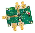
temperature range. An evaluation board is also available.
Document Feedback
Information furnished by Analog Devices is believed to be accurate and reliable. However, no
responsibility is assumed by Analog Devices for its use, nor for any infringements of patents or other
rights of third parties that may result from its use. Specifications subject to change without notice. No
license is granted by implication or otherwise under any patent or patent rights of Analog Devices.
Trademarks and registered trademarks are the property of their respective owners.
One Technology Way, P.O. Box 9106, Norwood, MA 02062-9106, U.S.A.
Tel: 781.329.4700 ©2005–2016 Analog Devices, Inc. All rights reserved.
Technical Support
www.analog.com
�AD8342
Data Sheet
TABLE OF CONTENTS
Features .............................................................................................. 1
Test Circuit ...................................................................................... 14
Applications ....................................................................................... 1
Theory of Operation ...................................................................... 15
Functional Block Diagram .............................................................. 1
AC Interfaces ................................................................................... 16
General Description ......................................................................... 1
IF Port .......................................................................................... 17
Revision History ............................................................................... 2
LO Considerations ..................................................................... 18
Specifications..................................................................................... 3
High Frequency Applications ................................................... 19
AC Performance ........................................................................... 4
Applications Above 3 GHz ........................................................ 20
Absolute Maximum Ratings ............................................................ 5
Low Frequency Applications .................................................... 21
Junction to Board Thermal Impedance..................................... 5
Evaluation Board ............................................................................ 22
ESD Caution .................................................................................. 5
Outline Dimensions ....................................................................... 25
Pin Configuration and Function Descriptions ............................. 6
Ordering Guide .......................................................................... 25
Typical Performance Characteristics ............................................. 7
Spurious Performance................................................................ 13
REVISION HISTORY
3/16—Rev. B to Rev. C
Changes to Product Title ................................................................. 1
Changes to Table 2 ............................................................................ 4
Changes to Table 3 ............................................................................ 5
Added Junction to Board Thermal Impedance Section .............. 5
Changes to Figure 2 and Table 4 ..................................................... 6
Change to Typical Performance Characteristics Section ............ 7
Moved Spur Table Section and Table 3, Renumbered
Sequentially ..................................................................................... 13
Changed Spur Table Section to Spurious Performance Section ..... 13
Added Test Circuit Section............................................................ 14
Moved Figure 38 ............................................................................. 14
Changed Circuit Description Section to Theory of Operation
Section .............................................................................................. 15
Changes to Theory of Operation Section .................................... 15
Added Applications Above 3 GHz Section ................................. 20
Added Figure 56, Figure 57, and Figure 58, Renumbered
Sequentially ..................................................................................... 21
Updated Outline Dimensions ....................................................... 25
Changes to Ordering Guide .......................................................... 25
7/09—Rev. A to Rev. B
Changed RF and LO Frequency Range from 2.4 GHz to
3 GHz Throughout ............................................................................1
Changes to General Description Section .......................................1
Added Endnote 2 ...............................................................................4
Added Low Frequency Applications Section .............................. 19
Added Figure 56 and Figure 57 .................................................... 20
Changes to the Evaluation Board Section ................................... 21
Added Figure 59 to Figure 62 ....................................................... 22
Updated Outline Dimensions ....................................................... 24
Changes to Ordering Guide .......................................................... 24
1/07—Rev. 0 to Rev. A
Changes to Features ..........................................................................1
Changes to General Description .....................................................1
Changes to Table 2.............................................................................4
Replaced the High Frequency Applications Section.................. 18
4/05—Revision 0: Initial Version
Rev. C | Page 2 of 25
�Data Sheet
AD8342
SPECIFICATIONS
VS = 5 V, TA = 25°C, fRF = 238 MHz, fLO = 286 MHz, LO power = 0 dBm, ZO = 50 Ω, RBIAS = 1.82 kΩ, RF termination = 100 Ω, IF load =
100 Ω differential, unless otherwise noted.
Table 1.
Parameter
RF INPUT INTERFACE
Return Loss
Input Impedance
DC Bias Level
OUTPUT INTERFACE
Output Impedance
DC Bias Voltage
Power Range
LO INTERFACE
Return Loss
DC Bias Voltage
POWER-DOWN INTERFACE
PWDN Threshold
PWDN Response Time
PWDN Input Bias Current
POWER SUPPLY
Positive Supply Voltage
Quiescent Current
VPDC
VPMX, IFOP, IFOM
VPLO
Total Quiescent Current
Power-Down Current
Test Conditions/Comments
Min
High-Z input terminated with 100 Ω off-chip resistor
Frequency = 238 MHz (measured at RFIN with RFCM ac-grounded)
Internally generated; port must be ac-coupled
Differential impedance, frequency = 48 MHz
Supplied externally
Via a 2:1 impedance ratio transformer
Typ
Max
10
1||0.4
2.4
4.75
10||0.5
VS
Unit
dB
kΩ||pF
V
5.25
13
kΩ||pF
V
dBm
Internally generated; port must be ac-coupled
10
VS − 1.6
dB
V
Device enabled, IF output to 90% of its final level
Device disabled, supply current
很抱歉,暂时无法提供与“AD8342-EVALZ”相匹配的价格&库存,您可以联系我们找货
免费人工找货