800 MHz, Linear-in-dB VGA with AGC Detector AD8368
FEATURES
Analog variable gain range: −12 dB to +22 dB Linear-in-dB scaling: 37.5 dB/V 3 dB bandwidth: 800 MHz @ VGAIN = 0.5 V Integrated rms detector P1dB: 16 dBm @ 140 MHz Output IP3: 33 dBm @ 140 MHz Noise figure at maximum gain: 9.5 dB @ 140 MHz Input and output impedances: 50 Ω Single-supply voltage from 4.5 V to 5.5 V RoHS-compliant, 24-lead LFCSP
ICOM 16 OCOM 6 GAIN 1 OCOM 7 gm STAGES 0dB –2dB INPT 19 ICOM 17 ICOM 18 ICOM 20 50Ω DECL ATTENUATOR LADDER –4dB –36dB REF
–
FUNCTIONAL BLOCK DIAGRAM
VPSO
10
MODE
21
VPSO VPSI VPSI VPSI VPSI VPSI
9 11 12 22 23 13
AD8368
GAIN INTERPOLATOR FIXED-GAIN AMPLIFIER OUTPUT BUFFER
24 ENBL 8 3 4
OUTP HPFL DECL
14 DECL
X2
+ 2 5
15 DECL
APPLICATIONS
Complete IF AGC amplifiers Gain trimming and leveling Cellular base stations Point-to-point radio links RF instrumentation
Figure 1.
DETO
DETI
GENERAL DESCRIPTION
The AD8368 is a variable gain amplifier (VGA) with analog linear-in-dB gain control that can be used from low frequencies to 800 MHz. Its excellent gain range, conformance, and flatness are attributed to the Analog Devices, Inc. X-AMP® architecture, an innovative technique for implementing high performance variable gain control. The gain range of −12 dB to +22 dB is scaled accurately to 37.5 dB/V with excellent conformance error. The AD8368 has a 3 dB bandwidth of 800 MHz that is nominally independent of gain setting. At 140 MHz, the OIP3 is 33 dBm at maximum gain. The output noise floor is −143 dBm/Hz, which corresponds to a 9.5 dB noise figure at maximum gain. The single-ended input and output impedances are nominally 50 Ω. The gain of the AD8368 can be configured to be an increasing or decreasing function of the gain control voltage depending on whether the MODE pin is pulled to the positive supply or to ground, respectively. When MODE is pulled high, the AD8368 operates as a typical VGA with increasing gain. By connecting MODE to ground and using the on-board rms detector, the AD8368 can be configured as a complete AGC system with RSSI. The output power is accurately leveled to the internal default setpoint of 63 mV rms (−11 dBm referenced to 50 Ω), independent of the waveform crest factor. Because the uncommitted detector input is available at DETI, the AGC loop can level the signal at the AD8368 output or at any other point in the signal chain over a maximum input power range of 34 dB. Furthermore, the setpoint level can be raised by dividing down the output signal before applying it to the detector. The AD8368 operates from a supply voltage of 4.5 V to 5.5 V and consumes 60 mA of current. It can be fully powered down to 30 dB range of input levels.
10 5 0
Figure 36 shows a plot of the RSSI voltage at DETO as input power is swept.
3.0
2.5
2.0
RSSI (V)
1.5
1.0
0.5
05907-039
POWER OUT (dBm)
–5 –10 –15 –20
05907-038
0 –40
–30
–20
–10 POWER IN (dBm)
0
10
20
Figure 36. Monitoring the GAIN/DETO RSSI Voltage vs. Input Power
–25 –30 –40
In some cases, it can be found that, if driven into AGC overload, the AD8368 requires unusually long times to recover; that is, the voltage at DETO remains at an abnormally high value, and the gain is at its lowest value. To avoid this situation, it is recommended that a clamp be placed on the DETO pin, as shown in Figure 37.
ICOM ICOM ICOM DECL DECL VPSI
–30
–20
–10 POWER IN (dBm)
0
10
20
Figure 35. Output Power vs. Input Power in AGC Mode at 140 MHz
Note that to achieve the accurate level of AGC output power, the DECL capacitor must be adjusted for the corresponding RF frequency. The DECL capacitor value varies depending on board parasitics. Table 5 shows the DECL capacitor value based on the evaluation board parasitics.
Table 5. DECL Capacitor Value
IF Frequency (MHz) 70 140 240 380 480 C4 (pF) 1000 270 68 33 15 C20 (pF) 2200 560 150 68 39
CAGC 0.1µF
INPT ICOM MODE VPSI VPSI ENBL
OCOM DETO DECL HPFL GAIN DETI
VPSI VPSI VPSO
AD8368
VPSO OUTP OCOM
+VS
VAGC
RB 0.5V RA
05907-042
Q1 2N2907
A valuable feature of using a square law detector in AGC mode is that the RSSI voltage is a true reflection of signal power and can be converted to an absolute power measurement for any given source impedance. The RSSI in units of dBm referenced to 50 Ω and based on the voltage available on the DETO pin is given by
RSSI = −11 + 20 log10(1 + R1/R2) + 38 × VDETO − 24.8
Figure 37. External Clamp to Prevent AGC Overload
The resistive divider network, RA and RB, should be designed such that the base of Q1 is driven to 0.5 V.
Rev. A | Page 15 of 20
�AD8368
The choice of CDETO is a compromise of averaging time constant, response time, and carrier leakage. If CDETO is selected to be too small to speed up the response time, the AGC loop could start tracking and leveling any amplitude envelope and corrupt the constellation. Figure 38 illustrates a 16 QAM, 100 ksymbols per second constellation with a degraded error vector magnitude (EVM) of 5%. By increasing CDETO to 0.01 μF, the EVM is improved to 1.1%.
REF –4.9dBm SR 10kHz CF 100MHz 16 QAM MEAS SIGNAL CONST DIAG
Figure 39 illustrates the measured EVM performance for a 16 QAM modulation at 10 Msymbols per second using CDETO = 1 nF.
10 9 8 7
EVM (%)
6 5 4 3 2 1 0 –40 –30 –20 –10 POWER IN (dBm) 0 10 20
05907-041
1U
Figure 39. Error Vector Magnitude Performance for 16 QAM 10 Msymbols per second
05907-040
–1U –1.31289U 262.578mU/ 1.31289U
Figure 38. Degraded Error Vector Magnitude Performance for 16 QAM at 100 ksymbols per second (CDETO Too Small)
Rev. A | Page 16 of 20
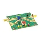
�AD8368 EVALUATION BOARD
VPOS C20 1nF VPOS1 VPOS2 VPOS3
ICOM ICOM ICOM DECL
INPUT R1 10kΩ LOW VPOS1 C13 0.1µF ENABLE HI
CIN 10nF INPT ICOM SW1 MODE VPSI VPSI ENBL
DECL
VPSI
VPSI VPSI VPSO
R11 0Ω C11 1nF R12 0Ω COUT 10nF OUTPUT C12 1nF
VPOS2 C14 0.1µF VPOS3 C15 0.1µF
AD8368
R10 0Ω SW2 C10 1nF
VPSO OUTP OCOM
OCOM
ON OFF R2 10kΩ
DETO
DECL
HPFL
GAIN
GAIN GAIN DET_OUT_TP R35 OPEN JP4 C23 10nF R32 OPEN C6 1nF C4 1nF
DETI
R31 OPEN
Figure 40. Evaluation Board
Table 6. Evaluation Board Configuration Options
Component R1, R2 R10, R11, R12, C10, C11, C12, C13, C14, C15 CIN COUT R31, R32 Function Pull-Down Resistors for MODE and ENBL. Supply Decoupling. Jumpers, power supply decoupling resistors, and filter capacitors. Default Conditions R1 = R2 = 10 kΩ R10 = R11 = R12 = 0 Ω C10 = C11 = C12 = 1 nF C13 = C14 = C15 = 0.1 μF CIN = 10 nF COUT = 10 nF R31 = R32 = Open (VGA mode)
R35 C23 C1, R30 C6 C20, C4 JP4 SW1 SW2
RF Input. CIN provides dc block for RF input. RF Output. COUT provides dc block for RF output. Feedback Path for AGC Operation. For a default setpoint of 63 mV rms, set R31 = 0 Ω and remove R32. For other AGC setpoints, rms voltage = (1 + n) × 63 mV rms, where n = R31/R32. Populate with 0 Ω to feed detector output RSSI voltage to DET_OUT_TP. Sets the corner frequency of the output offset control loop high-pass filter. Used for driving the detector externally. Set R30 to 50 Ω for matching. Set C1 to be a large ac coupling capacitor. DETO Capacitor. Needs to be made larger for lower data rates (see the AGC Operation section). DECL Capacitor. Needs to be adjusted based on RF frequency in AGC operation (see the AGC Operation section). Jumper for AGC Mode of Operation. Provides feedback from the detector output to the gain pin. Mode Switch. Low mode puts the part in gain-down mode. High puts the part in gain-up mode. AGC operation requires gain-down mode. Power-Down. The part is disabled when the enable pin is tied to ground.
R35 = Open C23 = 10 nF C1 = Open R30 = Open C6 = 1 nF C20 = C4 = 1 nF JP4 = not populated (VGA mode) SW1 = JP2 SW2 = JP3
Rev. A | Page 17 of 20
05907-043
C1 OPEN
R30 OPEN
DET_IN
�AD8368 OUTLINE DIMENSIONS
4.00 BSC SQ 0.60 MAX 0.60 MAX 0.50 BSC 0.50 0.40 0.30 1.00 0.85 0.80 12° MAX 0.80 MAX 0.65 TYP
19 18 EXPOSED PAD 24 1
PIN 1 INDICATOR 2.65 2.50 SQ 2.35
6
PIN 1 INDICATOR
TOP VIEW
3.75 BSC SQ
(BO TTOMVIEW)
13 12
7
0.23 MIN 2.50 REF
0.05 MAX 0.02 NOM 0.20 REF COPLANARITY 0.08
SEATING PLANE
0.30 0.23 0.18
COMPLIANT TO JEDEC STANDARDS MO-220-VGGD-8
Figure 41. 24-Lead Lead Frame Chip Scale Package [LFCSP_VQ] 4 mm × 4 mm Body, Very Thin Quad (CP-24-3) Dimensions shown in millimeters
ORDERING GUIDE
Model AD8368ACPZ-REEL7 1 AD8368ACPZ-WP1, 2 AD8368-EVALZ1
1 2
Temperature Range −40°C to +85°C −40°C to +85°C
Package Description 24-Lead Lead Frame Chip Scale Package (LFCSP_VQ) 24-Lead Lead Frame Chip Scale Package (LFCSP_VQ) Evaluation Board
Package Option CP-24-3 CP-24-3
Ordering Quantity 1,500 64
Z = RoHS Compliant Part. WP = waffle pack.
Rev. A | Page 18 of 20
�AD8368 NOTES
Rev. A | Page 19 of 20
�AD8368 NOTES
©2006-2007 Analog Devices, Inc. All rights reserved. Trademarks and registered trademarks are the property of their respective owners. D05907-0-10/07(A)
Rev. A | Page 20 of 20
�


 工商网监
湘ICP备2023018690号
工商网监
湘ICP备2023018690号