a
FEATURES AC PERFORMANCE Gain Bandwidth Product: 80 MHz (Gain = 2) Fast Settling: 100 ns to 0.01% for a 10 V Step Slew Rate: 375 V/ s Stable at Gains of 2 or Greater Full Power Bandwidth: 6.0 MHz for 20 V p-p DC PERFORMANCE Input Offset Voltage: 1 mV max Input Offset Drift: 14 V/ C Input Voltage Noise: 9 nV/√Hz typ Open-Loop Gain: 90 V/mV into a 500 Load Output Current: 100 mA min Quiescent Supply Current: 14 mA max APPLICATIONS Line Drivers DAC and ADC Buffers Video and Pulse Amplifiers Available in Plastic DIP, Hermetic Metal Can, Hermetic Cerdip, SOIC and LCC Packages and in Chip Form MIL-STD-883B Parts Available Available in Tape and Reel in Accordance with EIA-481A Standard PRODUCT DESCRIPTION
Wideband, High Output Current, Fast Settling Op Amp AD842*
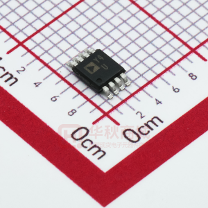
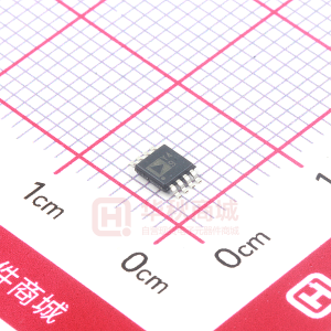
CONNECTION DIAGRAMS Plastic DIP (N) Package and Cerdip (Q) Package
NC 1 NC 2 BALANCE 3 –INPUT 4 +INPUT 5 V– 6 NC 7 TOP VIEW
+ 14 13 12 11 10 9 8
LCC (E) Package
2 BALANCE 20 BALANCE
3 NC
1 NC
AD842
NC BALANCE NC V+ OUTPUT NC NC
NC –IN NC +IN NC
19 NC
4 5 6 7 8
18 17 16
NC
+
AD842
NC 9 –VS 10 NC 11 NC 12 NC 13
+VS NC 15 OUTPUT 14 NC
NC = NO CONNECT
NC = NO CONNECT
TO-8 (H) Package
BALANCE BALANCE NC NC
SOIC (R-16) Package
NC 1
16 NC
V+
BALANCE 2 –INPUT 3
AD842
15 BALANCE 14 +V S 13 NC
AD842
–INPUT
+
OUTPUT
NC 4
+
+INPUT 5
12 OUTPUT 11 NC 10 NC
+INPUT
V– NC NC
NC 6 –VS 7 NC 8 TOP VIEW
The AD842 is a member of the Analog Devices family of wide bandwidth operational amplifiers. This device is fabricated using Analog Devices’ junction isolated complementary bipolar (CB) process. This process permits a combination of dc precision and wideband ac performance previously unobtainable in a monolithic op amp. In addition to its 80 MHz gain bandwidth, the AD842 offers extremely fast settling characteristics, typically settling to within 0.01% of final value in less than 100 ns for a 10 volt step. The AD842 also offers a low quiescent current of 13 mA, a high output current drive capability (100 mA minimum), a low input voltage noise of 9 nV√Hz and a low input offset voltage (1 mV maximum). The 375 V/µs slew rate of the AD842, along with its 80 MHz gain bandwidth, ensures excellent performance in video and pulse amplifier applications. This amplifier is ideally suited for use in high frequency signal conditioning circuits and wide bandwidth active filters. The extremely rapid settling time of the AD842 makes this amplifier the preferred choice for data acquisition applications which require 12-bit accuracy. The
*Covered by U.S. Patent Nos. 4,969,823 and 5,141,898.
NC
9
NC
TOP VIEW NOTE: CAN BE TIED TO V+ NC = NO CONNECT
NC = NO CONNECT
AD842 is also appropriate for other applications such as high speed DAC and ADC buffer amplifiers and other wide bandwidth circuitry.
APPLICATION HIGHLIGHTS
1. The high slew rate and fast settling time of the AD842 make it ideal for DAC and ADC buffers amplifiers, lines drivers and all types of video instrumentation circuitry. 2. The AD842 is a precision amplifier. It offers accuracy to 0.01% or better and wide bandwidth; performance previously available only in hybrids. 3. Laser-wafer trimming reduces the input offset voltage of 1 mV max, thus eliminating the need for external offset nulling in many applications. 4. Full differential inputs provide outstanding performance in all standard high frequency op amp applications where the circuit gain will be 2 or greater. 5. The AD842 is an enhanced replacement for the HA2542.
R EV. E
Information furnished by Analog Devices is believed to be accurate and reliable. However, no responsibility is assumed by Analog Devices for its use, nor for any infringements of patents or other rights of third parties which may result from its use. No license is granted by implication or otherwise under any patent or patent rights of Analog Devices. One Technology Way, P.O. Box 9106, Norwood, MA 02062-9106, U.S.A. Tel: 781/329-4700 World Wide Web Site: http://www.analog.com Fax: 781/326-8703 © Analog Devices, Inc., 2000
�AD842–SPECIFICATIONS (@ +25 C and
Model Conditions INPUT OFFSET VOLTAGE3 TMIN–TMAX Offset Drift INPUT BIAS CURRENT TMIN–TMAX Input Offset Current TMIN–TMAX INPUT CHARACTERISTICS Input Resistance Input Capacitance INPUT VOLTAGE RANGE Common Mode Common-Mode Rejection INPUT VOLTAGE NOISE Wideband Noise OPEN-LOOP GAIN Differential Mode 100 2.0 10 86 80 0.1 14 4.2 Min 0.5
15 V dc, unless otherwise noted)
AD842K Min Typ Max 0.3 14 8 10 0.4 0.5 3.5 0.05 5 6 0.2 0.3 1.0 1.5 Min AD842S2 Typ 0.5 14 4.2 0.1 8 12 0.4 0.6 Max 1.5 3.5 Units mV mV µV/°C µA µA µA µA kΩ pF V dB dB nV/√Hz µV rms V/mV V/mV V mA Ω MHz MHz ns % V/µs ns ns % Degree V V mA mA dB dB °C
AD842J/JR1 Typ Max 1.5 2.5/3
100 2.0 10 90 86 10 86 80
100 2.0
VCM = ± 10 V TMIN–TMAX f = 1 kHz 10 Hz to 10 MHz VO = ± 10 V RLOAD ≥ 500 Ω TMIN–TMAX RLOAD ≥ 500 Ω VOUT = ± 10 V Open Loop VOUT = 90 mV VO = 20 V p-p RLOAD ≥ 500 Ω AVCL = –2 AVCL = –2 AVCL = –2 10 V Step to 0.1% to 0.01% f = 4.4 MHz f = 4.4 MHz
115 9 28
115 9 28
115 9 28
40/30 20/15 10 100
90
50 25 10 100
90
40 20 10 100
90
OUTPUT CHARACTERISTICS Voltage Current FREQUENCY RESPONSE Gain Bandwidth Product Full Power Bandwidth4 Rise Time5 Overshoot5 Slew Rate5 Settling Time5
5 80 4.7 6 10 20 375 80 100 0.015 0.035 ± 15 5 13/14 18 14/16 16/19.5 5 4.7
5 80 6 10 20 375 80 100 0.015 0.035 ± 15 13 90 86 +75 0 AD842KN AD842KQ 105 18 14 16 5 4.7
5 80 6 10 20 375 80 100 0.015 0.035 ± 15 13 86 80 +75 –55 100 18 14 19
300
300
300
Differential Gain Differential Phase POWER SUPPLY Rated Performance Operating Range Quiescent Current Power Supply Rejection Ratio TEMPERATURE RANGE Rated Performance6 PACKAGE OPTIONS Plastic (N-14) Cerdip (Q-14) SOIC (R-16) Tape and Reel TO-8 (H-12A) LCC (E-20A) Chips
TMIN–TMAX VS = ± 5 V to ± 18 V TMIN–TMAX
86 80 0
100
+125
AD842JN AD842JQ AD842JR-16 AD842JR-16-REEL AD842JR-16-REEL7 AD842JH AD842JCHIPS
AD842SQ, AD842SQ/883B
AD842KH
AD842SH AD842SE/883B AD842SCHIPS
NOTES 1 AD842JR specifications differ from those of the AD842JN, JQ and JH due to the thermal characteristics of the SOIC package. 2 Standard Military Drawing available 5962-8964201xx 2A – (SE/883B); XA – (SH/883B); CA – (SQ/883B). 3 Input offset voltage specifications are guaranteed after 5 minutes at TA = +25°C. 4 Full power bandwidth = slew rate/2 π VPEAK. 5 Refer to Figures 22 and 23. 6 “S” grade TMIN–TMAX specifications are tested with automatic test equipment at TA = –55°C and TA = +125°C. All min and max specifications are guaranteed. Specifications shown in boldface are tested on all production units. Specifications subject to change without notice.
– 2–
REV. E
�AD842
ABSOLUTE MAXIMUM RATINGS 1
Supply Voltage . . . . . . . . . . . . . . . . . . . . . . . . . . . . . . . . ± 18 V Internal Power Dissipation2 Plastic (N) . . . . . . . . . . . . . . . . . . . . . . . . . . . . . . . . . 1.3 W Cerdip (Q) . . . . . . . . . . . . . . . . . . . . . . . . . . . . . . . . . 1.1 W TO-8 (H) . . . . . . . . . . . . . . . . . . . . . . . . . . . . . . . . . . 1.3 W SOIC (R) . . . . . . . . . . . . . . . . . . . . . . . . . . . . . . . . . . 1.3 W LCC (E) . . . . . . . . . . . . . . . . . . . . . . . . . . . . . . . . . . 1.0 W Input Voltage . . . . . . . . . . . . . . . . . . . . . . . . . . . . . . . . . . . ± VS Differential Input Voltage . . . . . . . . . . . . . . . . . . . . . . . . ± 6 V Storage Temperature Range Q, H, E . . . . . . . . . . . . . . . . . . . . . . . . . . –65°C to +150°C N, R . . . . . . . . . . . . . . . . . . . . . . . . . . . . . –65°C to +125°C Junction Temperature . . . . . . . . . . . . . . . . . . . . . . . . . +175°C Lead Temperature Range (Soldering 60 sec) . . . . . . . . +300°C
NOTES 1 Stresses above those listed under Absolute Maximum Ratings may cause permanent damage to the device. This is a stress rating only; functional operation of the device at these or any other conditions above those indicated in the operational section of this specification is not implied. Exposure to absolute maximum rating conditions for extended periods may affect device reliability. 2 Maximum internal power dissipation is specified so that T J does not exceed +150°C at an ambient temperature of +25 °C. Thermal Characteristics: θJC θJA θSA Plastic Package 30°C/W 100°C/W Cerdip Package 30°C/W 110°C/W 38°C/W TO-8 Package 30°C/W 100°C/W 27°C/W 16-Lead SOIC Package 30°C/W 100°C/W 20-Lead LCC Package 35°C/W 150°C/W Recommended Heat Sink: Aavid Engineering© #602B
METALIZATION PHOTOGRAPH
Contact factory for latest dimensions. Dimensions shown in inches and (mm).
REV. E
–3–
�AD842–Typical Characteristics (at +25 C and V =
S
20 20
15 V, unless otherwise noted)
30
OUTPUT VOLTAGE SWING – Volts p-p
INPUT COMMON-MODE RANGE – Volts
OUTPUT VOLTAGE SWING – Volts
25 15V SUPPLIES 20 15
15 VIN 10
15 VOUT
10
10
5
5
5 0
0
0
5 10 SUPPLY VOLTAGE –
15 Volts
20
0
0
5 10 SUPPLY VOLTAGE –
15 Volts
20
10
100 1k LOAD RESISTANCE –
10k
Figure 1. Input Common-Mode Range vs. Supply Voltage
Figure 2. Output Voltage Swing vs. Supply Voltage
Figure 3. Output Voltage Swing vs. Load Resistance
18
–5
100
QUIESCENT CURRENT – mA
INPUT BIAS CURRENT – A
–4
OUTPUT IMPEDANCE –
16
10
14
1
–3
12
0.1
10
0
5 10 SUPPLY VOLTAGE –
15 Volts
20
–2 –60 –40 –20
0 20 40 60 80 100 120 140 TEMPERATURE – C
0.01 10k
1M 10M 100k FREQUENCY – Hz
100M
Figure 4. Quiescent Current vs. Supply Voltage
Figure 5. Input Bias Current vs. Temperature
Figure 6. Output Impedance vs. Frequency
18
SHORT CIRCUIT CURRENT LIMIT – mA
300 275
GAIN BANDWIDTH – MHz
85
17
QUIESCENT CURRENT – mA
16 15 14 13 12 11 10 –60 –40 –20
250 + OUTPUT CURRENT 225 200 175 –OUTPUT CURRENT 150 125 100 –60 –40 –20 0 20 40 60 80 100 120 140 AMBIENT TEMPERATURE – C
80
75
70
0 20 40 60 80 100 120 140 TEMPERATURE – C
65 –60 –40 –20
0 20 40 60 80 100 120 140 TEMPERATURE – C
Figure 7. Quiescent Current vs. Temperature
Figure 8. Short-Circuit Current Limit vs. Temperature
Figure 9. Gain Bandwidth Product vs. Temperature
–4–
REV. E
�AD842
120 100 100 80 110 120
POWER SUPPLY REJECTION – dB
100 + SUPPLY 80
PHASE MARGIN – Degrees
OPEN-LOOP GAIN – dB
80 60
60 40
OPEN-LOOP GAIN – dB
105
100 500 95 LOAD
60 – SUPPLY 40
40 500 20 0 100 LOAD
20
0
20 0 100
1k
10k 100k 1M FREQUENCY – Hz
10M
100M
90
0
5 10 15 SUPPLY VOLTAGE – V
20
1k
10k 100k 1M FREQUENCY – Hz
10M 100M
Figure 10. Open-Loop Gain and Phase Margin vs. Frequency
Figure 11. Open-Loop Gain vs. Supply Voltage
Figure 12. Power Supply Rejection vs. Frequency
120
30
10
RL = 1kV +25 C VS = 15V
OUTPUT VOLTAGE – Volts p-p
OUTPUT SWING FROM 0 TO
100
VS = 15V VCM = 1V p-p + 25 C
25
V
8 6 4 2 0.1% 0.01% 0 0.1% 0.01% –2 –4 –6 –8
20
CMR – dB
80
15
60
10
40
5 0 1M
20
–10
10M FREQUENCY – Hz 100M
1k
10k
100k 1M 10M FREQUENCY – Hz
100M
30
40
50 60 70 80 90 SETTLING TIME – ns
100 110
Figure 13. Common-Mode Rejection vs. Frequency
Figure 14. Large Signal Frequency Response
Figure 15. Output Swing and Error vs. Settling Time
–80
3V RMS RL = 1k
50
550
HARMONIC DISTORTION – dB
–90
INPUT VOLTAGE – nV Hz
40
500
–100 2ND HARMONIC
SLEW RATE – V s
450 400
30
–110
20
–120 3RD HARMONIC
350
–130 –140 100
10
300 250 –60 –40 –20
1k 10k FREQUENCY – Hz
100k
0 10
100
1k 10k 100k FREQUENCY – Hz
1M
10M
0 20 40 60 80 100 120 140 TEMPERATURE – C
Figure 16. Harmonic Distortion vs. Frequency
Figure 17. Input Voltage vs. Frequency
Figure 18. Slew Rate vs. Temperature
REV. E
–5–
�AD842
RF = 1k 0.1 F +VS HP3314A FUNCTION GENERATOR OR EQUIVALENT RIN = 499 49.9 2.2 F
– AD842 +
VOUT 0.1 F 499
332 2.2 F –VS
Figure 19a. Inverting Amplifier Configuration (DIP Pinout)
Figure 19b. Inverter Large Signal Pulse Response
Figure 19c. Inverter Small Signal Pulse Response
R1 = 205
RF = 205 0.1 F +VS 2.2 F
HP3314A FUNCTION VIN GENERATOR OR EQUIVALENT
100 49.9
– AD842 +
VOUT 0.1 F 499
2.2 F –VS
Figure 20a. Noninverting Amplifier Configuration (DIP Pinout)
Figure 20b. Noninverting Large Signal Pulse Response
Figure 20c. Noninverting Small Signal Pulse Response
–6–
REV. E
�AD842
OFFSET NULLING
The input offset voltage of the AD842 is very low for a high speed op amp, but if additional nulling is required, the circuit shown in Figure 21 can be used.
AD842 SETTLING TIME
ERROR AMP ( 15)
TEK 7A13 TEK 7603 OSCILLOSCOPE TEK 7A16
Figures 22 and 24 show the settling performance of the AD842 in the test circuit shown in Figure 23. Settling time is defined as: The interval of time from the application of an ideal step function input until the closed-loop amplifier output has entered and remains within a specified error band. This definition encompasses the major components which comprise settling time. They include (1) propagation delay through the amplifier; (2) slewing time to approach the final output value; (3) the time of recovery from the overload associated with slewing and (4) linear settling to within the specified error band. Expressed in these terms, the measurement of settling time is obviously a challenge and needs to be done accurately to assure the user that the amplifier is worth consideration for the application.
+VS 10k 2.2 F
DDD5109 FLAT-TOP PULSE GENERATOR 499 1k 499 50 1k
HP6263
0.1 F +15V 2.2 F FET PROBE TEK P6201 0.1 F 499 2.2 F –15V 499
AD842
Figure 23. Settling Time Test Circuit
0.1 F
INPUT
– AD842 +
OUTPUT 0.1 F RL
2.2 F –VS
Figure 23 shows how measurement of the AD842’s 0.01% settling in 100 ns was accomplished by amplifying the error signal from a false summing junction with a very high-speed proprietary hybrid error amplifier specially designed to enable testing of small settling errors. The device under test was driving a 300 Ω load. The input to the error amp is clamped in order to avoid possible problems associated with the overdrive recovery of the oscilloscope input amplifier. The error amp gains the error from the false summing junction by 15, and it contains a gain vernier to fine trim the gain. Figure 24 shows the “long term” stability of the settling characteristics of the AD842 output after a 10 V step. There is no evidence of settling tails after the initial transient recovery time. The use of a junction isolated process, together with careful layout, avoids these problems by minimizing the effects of transistor isolation capacitance discharge and thermally induced shifts in circuit operating points. These problems do not occur even under high output current conditions.
Figure 21. Offset Nulling (DIP Pinout)
Figure 22. 0.01% Settling Time
REV. E
–7–
�AD842
GROUNDING AND BYPASSING USING A HEAT SINK
In designing practical circuits with the AD842, the user must remember that whenever high frequencies are involved, some
The AD842 draws less quiescent power than most precision high speed amplifiers and is specified for operation without a heat sink. However, when driving low impedance loads, the current to the load can be 10 times the quiescent current. This will create a noticeable temperature rise. Improved performance can be achieved by using a small heat sink such as the Aavid Engineering #602B.
TERMINATED LINE DRIVER
The AD842 is optimized for high speed line driver applications. Figure 25 shows the AD842 driving a doubly terminated cable in a gain-of-2 follower configuration. The AD842 maintains a typical slew rate of 375 V/µs, which means it can drive a ± 10 V, 6.0 MHz signal or a ± 3 V, 19.9 MHz signal.
Figure 24. AD842 Settling Demonstrating No Settling Tails
special precautions are in order. Circuits must be built with short interconnect leads. Large ground planes should be used whenever possible to provide a low resistance, low inductance circuit path, as well as minimizing the effects of high frequency coupling. Sockets should be avoided because the increased interlead capacitance can degrade bandwidth. Feedback resistors should be of low enough value to assure that the time constant formed with the circuit capacitances will not limit the amplifier performance. Resistor values of less than 5 kΩ are recommended. If a larger resistor must be used, a small (