Wideband, High Output Current
Fast Settling Op Amp
AD842
Data Sheet
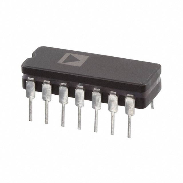
CONNECTION DIAGRAMS
AC performance
Gain bandwidth product: 80 MHz (gain = 2)
Fast settling: 100 ns to 0.01% for a 10 V step
Slew rate: 375 V/µs
Stable at gains of 2 or greater
Full power bandwidth: 6 MHz for 20 V p-p
DC performance
Input offset voltage: 1.5 mV maximum
Input offset drift: 14 µV/°C
Input voltage noise: 9 nV/√Hz
Open-loop gain: 90 V/mV into a 499 Ω load
Output current: 100 mA minimum
Quiescent supply current: 14 mA maximum
NIC
1
NIC
2
BALANCE
–INPUT
+INPUT
5
V–
NIC
14
NIC
13
BALANCE
3
12
NIC
4
11
V+
10
OUTPUT
6
9
NIC
7
(Not to Scale) 8
NIC
AD842
TOP VIEW
+
09477-001
FEATURES
NOTES
1. NIC = NOT INTERNALLY CONNECTED.
Figure 1. PDIP (N-14) and CERDIP (Q-14)
2
–INPUT 3
APPLICATIONS
AD842 16 NIC
TOP VIEW
15 BALANCE
(Not to Scale)
14 +VS
NIC 4
13
NIC
+INPUT 5
12
OUTPUT
11
NIC
7
10
NIC
NIC 8
9
NIC
+
NIC 6
Line drivers
DAC and ADC buffers
Video and pulse amplifiers
MIL-STD-883B parts available, see military data sheet
–VS
NOTES
1. NIC = NOT INTERNALLY CONNECTED.
09477-002
NIC 1
BALANCE
Figure 2. SOIC_W (RW-16)
GENERAL DESCRIPTION
The AD842 is a member of the Analog Devices, Inc. family of
wide bandwidth operational amplifiers. This device is fabricated
using the Analog Device junction isolated complementary
bipolar (CB) process. This process permits a combination of dc
precision and wideband ac performance previously unobtainable in a monolithic op amp. In addition to its 80 MHz gain
bandwidth product, the AD842 offers extremely fast settling
characteristics, typically settling to within 0.01% of final value
in less than 100 ns for a 10 V step.
The AD842 also offers a low quiescent current of 13 mA, a high
output current drive capability (100 mA minimum), a low input
voltage noise of 9 nV√Hz, and a low input offset voltage
(1.5 mV maximum).
The 375 V/µs slew rate of the AD842, along with its 80 MHz
gain bandwidth product, ensures excellent performance in
video and pulse amplifier applications. This amplifier is ideally
suited for use in high frequency signal conditioning circuits and
wide bandwidth active filters. The extremely rapid settling time
of the AD842 makes this amplifier the preferred choice for data
Rev. F
acquisition applications requiring 12-bit accuracy. The AD842
is also appropriate for other applications, such as high speed
DAC and ADC buffer amplifiers and other wide bandwidth
circuitry.
PRODUCT HIGHLIGHTS
1.
2.
3.
4.
The high slew rate and fast settling time of the AD842
make it ideal for DAC and ADC buffers amplifiers, line
drivers, and all types of video instrumentation circuitry.
The AD842 is a precision amplifier. It offers accuracy to
0.01% or better and wide bandwidth, performance
previously available only in hybrids.
Laser-wafer trimming reduces the input offset voltage of
1.5 mV maximum, thus eliminating the need for external
offset nulling in many applications.
Full differential inputs provide outstanding performance in
all standard high frequency op amp applications where the
circuit gain is 2 or greater.
Document Feedback
Information furnished by Analog Devices is believed to be accurate and reliable. However, no
responsibility is assumed by Analog Devices for its use, nor for any infringements of patents or other
rights of third parties that may result from its use. Specifications subject to change without notice. No
license is granted by implication or otherwise under any patent or patent rights of Analog Devices.
Trademarks and registered trademarks are the property of their respective owners.
One Technology Way, P.O. Box 9106, Norwood, MA 02062-9106, U.S.A.
Tel: 781.329.4700 ©1988–2014 Analog Devices, Inc. All rights reserved.
Technical Support
www.analog.com
�AD842
Data Sheet
TABLE OF CONTENTS
Features .............................................................................................. 1
Typical Performance Characteristics ..............................................5
Applications ....................................................................................... 1
Theory of Operation .........................................................................9
Connection Diagrams ...................................................................... 1
Offset Nulling ................................................................................9
General Description ......................................................................... 1
Settling Time ..................................................................................9
Product Highlights ........................................................................... 1
Grounding and Bypassing ......................................................... 10
Revision History ............................................................................... 2
Capacitive Load Driving Ability............................................... 10
Specifications..................................................................................... 3
Using a Heat Sink ....................................................................... 10
Electrical Characteristics−±15 V Operation ............................ 3
Terminated Line Driver ............................................................. 10
Absolute Maximum Ratings ............................................................ 4
Overdrive Recovery ................................................................... 11
Thermal Characteristics .............................................................. 4
Outline Dimensions ....................................................................... 12
ESD Caution .................................................................................. 4
Ordering Guide .......................................................................... 13
Metalization Photograph ............................................................. 4
REVISION HISTORY
2/14—Rev. E to Rev. F
Updated Format .................................................................. Universal
Deleted 20-Terminal LCC and 12-Pin TO-8 .................. Universal
Changed NC Pin to NIC Pin Throughout .................................... 1
Changes to Features, General Description, Connection
Diagrams, and Product Highlights Sections ................................. 1
Changes to Table 1 ............................................................................ 3
Changes to Table 2, Thermal Characteristics Section, Table 3,
and Figure 3 ....................................................................................... 4
Changes to Figure 11, Figure 13, Figure 14, and Figure 15 ........ 6
Changes to Figure 18.........................................................................7
Changes to Figure 22 Caption, Figure 23 Caption, Figure 24,
and Figure 27......................................................................................8
Changes to Figure 28.........................................................................9
Changes to Using a Heat Sink Section and Figure 32................ 10
Changes to Figure 34...................................................................... 11
Updated Outline Dimensions ....................................................... 12
Added Ordering Guide .................................................................. 13
3/00—Rev. D to Rev. E
Rev. F | Page 2 of 16
�Data Sheet
AD842
SPECIFICATIONS
ELECTRICAL CHARACTERISTICS—±15 V OPERATION
TA = 25°C, unless otherwise specified. All minimum and maximum specifications are guaranteed. Specifications shown in boldface are
tested on all production units.
Table 1.
Parameter
INPUT OFFSET VOLTAGE 2
Test Conditions/
Comments
TMIN to TMAX
Offset Drift
INPUT BIAS CURRENT
TMIN to TMAX
Input Offset Current
INPUT CHARACTERISTICS
Input Resistance
Input Capacitance
INPUT VOLTAGE RANGE
Common Mode
Common-Mode Rejection
INPUT VOLTAGE NOISE
Wideband Noise
OPEN-LOOP GAIN
OUTPUT CHARACTERISTICS
Voltage
Current
FREQUENCY RESPONSE
Gain Bandwidth Product
Full Power Bandwidth 3
Rise Time
Overshoot
Slew Rate
Settling Time 4
Differential Gain
Differential Phase
POWER SUPPLY
Rated Performance
Operating Range
Quiescent Current
Power Supply Rejection
Ratio
TMIN to TMAX
Differential mode
AD842JN/AD842JQ/AD842JR 1
Min
Typ
Max
0.5
1.5
2.5/2.5/3
14
4.2
8
10
0.1
0.4
0.5
AD842KN/AD842KQ
Min
Typ
Max
0.3
1.0
1.5
14
3.5
5
6
0.05
0.2
0.3
100
2.0
VCM = ±10 V
TMIN to TMAX
f = 1 kHz
10 Hz to 10 MHz
VOUT = ±10 V
RLOAD ≥ 499 Ω
TMIN to TMAX
RLOAD ≥ 499 Ω
VOUT = ±10 V
Open loop
VOUT = 90 mV,
AVCL = 2
VOUT = 20 V p-p,
RLOAD ≥ 499 Ω
AVCL = −2
AVCL = −2
AVCL = −2
10 V step
To 0.1%
To 0.01%
f = 4.4 MHz
f = 4.4 MHz
±10
86
80
100
2.0
±10
90
86
115
9
28
40/40/30
20/20/15
50
25
±10
100
±10
86
80
115
40
20
90
Unit
mV
mV
µV/°C
µA
µA
µA
µA
kΩ
pF
V
dB
dB
nV/√Hz
µV rms
115
9
28
±10
100
90
V/mV
V/mV
±10
100
5
5
5
V
mA
Ω
80
80
80
MHz
4.7
6
MHz
300
10
20
375
ns
%
V/µs
80
100
0.015
0.035
ns
ns
%
Degree
4.7
6
300
10
20
375
4.7
6
300
10
20
375
80
100
0.015
0.035
80
100
0.015
0.035
±15
13/13/14
86
AD842SQ
Typ
Max
0.5
1.5
3.5
14
4.2
8
12
0.1
0.4
0.6
100
2.0
9
28
90
±5
TMIN to TMAX
±VS = ±5 V to
±18 V
TMIN to TMAX
Min
±15
±18
14/14/16
16/16/19.5
100
±5
13
90
±15
±18
14
16
105
86
80
1
AD842JR specifications differ from those of the AD842JN and AD842JQ due to the thermal characteristics of the SOIC package.
Input offset voltage specifications are guaranteed after 5 minutes at TA = 25°C.
Full power bandwidth = slew rate/2 π V peak.
4
Refer to Figure 29 and Figure 30.
2
3
Rev. F | Page 3 of 16
±5
13
86
80
100
±18
14
19
V
V
mA
mA
dB
dB
�AD842
Data Sheet
ABSOLUTE MAXIMUM RATINGS
Stresses above those listed under Absolute Maximum Ratings
may cause permanent damage to the device. This is a stress
rating only; functional operation of the device at these or any
other conditions above those indicated in the operational
section of this specification is not implied. Exposure to absolute
maximum rating conditions for extended periods may affect
device reliability.
Table 2.
Parameter
Supply Voltage
Internal Power Dissipation1
PDIP (N-14), SOIC_W (RW-16)
CERDIP (Q-14)
Input Voltage
Differential Input Voltage
Operating Temperature Range
CERDIP (Q-14, AD842SQ Only)
PDIP (N-14), SOIC_W (RW-16),
CERDIP (Q-14, AD842JQ and
AD842KQ Only)
Storage Temperature Range
CERDIP (Q-14, All Models)
PDIP (N-14), SOIC_W (RW-16)
Junction Temperature
Lead Temperature (Soldering 60 sec)
1
Rating
±18 V
1.3 W
1.1 W
±VS
±6 V
THERMAL CHARACTERISTICS
−55°C to +125°C
0°C to 70°C
−65°C to +150°C
−65°C to +125°C
175°C
300°C
Table 3.
Package
14-Lead PDIP
14-Lead CERDIP
16-Lead SOIC_W
θJC
30
30
30
θJA
100
110
100
ESD CAUTION
Maximum internal power dissipation is specified so that TJ does not exceed
150°C at an ambient temperature of 25°C.
METALIZATION PHOTOGRAPH
0.106 (2.68)
BALANCE
V+
BALANCE
–INPUT
+INPUT
V–
Figure 3. Contact Factory for Latest Dimensions,
Dimensions Shown in Inches and (Millimeters)
Rev. F | Page 4 of 16
09477-003
OUTPUT
0.067
(1.69)
θSA
38
Unit
°C/W
°C/W
°C/W
�Data Sheet
AD842
TYPICAL PERFORMANCE CHARACTERISTICS
TA = 25°C and VS = ±15 V, unless otherwise noted.
QUIESCENT CURRENT (mA)
18
10
VIN
5
0
0
5
10
15
SUPPLY VOLTAGE (±V)
20
16
14
12
10
0
Figure 4. Input Common-Mode Range vs. Supply Voltage
10
15
SUPPLY VOLTAGE (±V)
20
Figure 7. Quiescent Current vs. Supply Voltage
–5
15
10
±VOUT
5
0
5
10
15
SUPPLY VOLTAGE (±V)
20
–3
–2
–60
09477-005
0
–4
Figure 5. Output Voltage Swing vs. Supply Voltage
–40
–20
0
20
40
60
80
TEMPERATURE (°C)
100
120
140
09477-008
INPUT BIAS CURRENT (µA)
20
OUTPUT VOLTAGE SWING (V)
5
09477-007
15
09477-004
INPUT COMMON-MODE RANGE (V)
20
Figure 8. Input Bias Current vs. Temperature
30
100
OUTPUT IMPEDANCE (Ω)
±15V SUPPLIES
20
15
10
10
1
0.1
0
10
100
1k
LOAD RESISTANCE (Ω)
10k
0.01
10k
Figure 6. Output Voltage Swing vs. Load Resistance
100k
1M
FREQUENCY (Hz)
10M
Figure 9. Output Impedance vs. Frequency
Rev. F | Page 5 of 16
100M
09477-009
5
09477-006
OUTPUT VOLTAGE SWING (V p-p)
25
�AD842
Data Sheet
18
120
100
100
80
80
60
60
40
OPEN-LOOP GAIN (dB)
14
13
12
40
20
11
–40
–20
0
20
40
60
80
TEMPERATURE (°C)
100
120
140
0
0
100
09477-010
10
–60
Figure 10. Quiescent Current vs. Temperature
10M
100M
110
275
OPEN-LOOP GAIN (dB)
250
+OUTPUT CURRENT
225
200
175
–OUTPUT CURRENT
150
105
100
499Ω LOAD
95
–20
0
20
40
60
80
TEMPERATURE (°C)
100
120
140
90
09477-011
–40
0
10
15
SUPPLY VOLTAGE (±V)
20
Figure 14. Open-Loop Gain vs. Supply Voltage
Figure 11. Short-Circuit Current Limit vs. Temperature
120
POWER SUPPLY REJECTION (dB)
85
80
75
–40
–20
0
20
40
60
80
TEMPERATURE (°C)
100
120
140
100
+VS
80
–VS
60
40
20
0
100
09477-012
70
65
–60
5
09477-014
125
100
–60
GAIN BANDWIDTH (MHz)
100k
1M
10k
FREQUENCY (Hz)
1k
Figure 13. Open-Loop Gain and Phase Margin vs. Frequency
300
SHORT-CIRCUIT CURRENT LIMIT (mA)
20
499Ω LOAD
09477-013
15
Figure 12. Gain Bandwidth Product vs. Temperature
1k
10k
100k
1M
FREQUENCY (Hz)
10M
Figure 15. Power Supply Rejection vs. Frequency
Rev. F | Page 6 of 16
100M
09477-015
QUIESCENT CURRENT (mA)
16
PHASE MARGIN (Degrees)
17
�Data Sheet
AD842
–80
3V rms
RL = 1kΩ
VS = ±15V
VCM = 1V p-p
TA = 25°C
–90
80
60
40
1k
10k
100k
1M
FREQUENCY (Hz)
10M
100M
SECOND HARMONIC
–110
–120
Figure 16. Common-Mode Rejection vs. Frequency
1k
10k
FREQUENCY (Hz)
100k
Figure 19. Harmonic Distortion vs. Frequency
30
50
RL = 1kΩ
TA = 25°C
VS = ±15V
40
INPUT VOLTAGE (nV√Hz)
25
OUTPUT VOLTAGE (V p-p)
THIRD HARMONIC
–130
–140
100
09477-016
20
–100
09477-019
100
HARMONIC DISTORTION (dB)
COMMON-MODE REJECTION (dB)
120
20
15
10
30
20
10
1M
10M
FREQUENCY (Hz)
100M
0
09477-017
0
10
100
1k
10k
100k
FREQUENCY (Hz)
1M
10M
09477-020
5
Figure 20. Input Voltage vs. Frequency
Figure 17. Large Signal Frequency Response
550
10
8
500
SLEW RATE (V/µs)
4
2
0.1%
0.01%
0.1%
0.01%
0
–2
–4
–6
450
400
350
300
–10
30
40
50
60
70
80
SETTLING TIME (ns)
90
100
110
250
–60
Figure 18. Output Swing vs. Settling Time
–40
–20
0
20
40
60
80
TEMPERATURE (°C)
100
Figure 21. Slew Rate vs. Temperature
Rev. F | Page 7 of 16
120
140
09477-021
–8
09477-018
OUTPUT SWING (V)
6
�AD842
Data Sheet
2V
2V
10%
10%
0%
0%
09477-022
100%
90%
Figure 22. Inverting Large Signal Pulse Response (see Figure 24)
50mV
50ns
09477-024
50ns
100%
90%
Figure 25. Noninverting Large Signal Pulse Response (see Figure 27)
50mV
10%
10%
0%
0%
09477-023
100%
90%
Figure 23. Inverting Small Signal Pulse Response (see Figure 24)
Figure 26. Noninverting Small Signal Pulse Response (see Figure 27)
RF = 1kΩ
RF = 205Ω
RF = 205Ω
0.1µF
0.1µF
+VS
+VS
2.2µF
4
49.9Ω
AD842
6
4
VOUT
10
FUNCTION VIN
GENERATOR
499Ω
5
332Ω
2.2µF
11
0.1µF
2.2µF
–VS
100Ω
49.9Ω
11
AD842
VOUT
10
499Ω
5
6
0.1µF
2.2µF
–VS
Figure 27. Noninverting Amplifier Configuration (PDIP)
Figure 24. Inverting Amplifier Configuration (PDIP)
Rev. F | Page 8 of 16
09477-027
RIN =
499Ω
09477-026
FUNCTION
GENERATOR
50ns
09477-025
50ns
100%
90%
�Data Sheet
AD842
THEORY OF OPERATION
OFFSET NULLING
10V
10mV
20ns
100%
90%
The input offset voltage of the AD842 is very low for a high
speed op amp, but if additional nulling is required, the circuit
shown in Figure 28 can be used.
OUTPUT:
10V/DIV
SETTLING TIME
OUTPUT
ERROR:
0.02%/DIV
Figure 29 and Figure 31 show the settling performance of the
AD842 in the test circuit shown in Figure 30.
Settling time is the interval of time from the application of an
ideal step function input until the closed-loop amplifier output
enters and remains within a specified error band.
10%
This definition encompasses the major components that
comprise settling time. They include the following:
•
Figure 29. 0.01% Settling Time
Figure 30 shows how measurement of the AD842 0.01% settling
in 100 ns is accomplished by amplifying the error signal from a
false summing junction with a very high speed proprietary
hybrid error amplifier specially designed to enable testing of
small settling errors. Under test, the device drives a 300 Ω load.
The input to the error amp is clamped to avoid possible
problems associated with the overdrive recovery of the
oscilloscope input amplifier. The error amp gains the error from
the false summing junction by 15, and it contains a gain vernier
to fine trim the gain.
Propagation delay through the amplifier.
Slewing time to approach the final output value.
Time of recovery from the overload associated with
slewing.
Linear settling to within the specified error band.
Expressed in these terms, the measurement of settling time
must be accurate to assure the user that the amplifier is worth
consideration for the application.
+VS
10kΩ
Figure 31 shows the long-term stability of the settling
characteristics of the AD842 output after a 10 V step. There is
no evidence of settling tails after the initial transient recovery
time. The use of a junction isolated process, together with
careful layout, avoids these problems by minimizing the effects
of transistor isolation capacitance discharge and thermally
induced shifts in circuit operating points. These problems do
not occur even under high output current conditions.
0.1µF
3
2.2µF
13
4
11
AD842
VIN
10
VOUT
5
6
0.1µF
RL
09477-028
2.2µF
–VS
Figure 28. Offset Nulling (PDIP)
ERROR
AMP
(×15)
TEK
7A13
TEK
7603
OSCILLOSCOPE
TEK
7A16
HP6263
DDD5109
FLAT-TOP
PULSE
GENERATOR
499Ω
1kΩ
499Ω
1kΩ
0.1µF
50Ω
+15V
2.2µF
4
11
AD842
5
499Ω
6
FET PROBE
TEK P6201
10
0.1µF
499Ω
2.2µF
–15V
Figure 30. Settling Time Test Circuit (PDIP)
Rev. F | Page 9 of 16
09477-030
•
•
•
09477-029
0%
�AD842
Data Sheet
GROUNDING AND BYPASSING
the dynamic performance of the device, although instability
does not occur unless the load exceeds 100 pF.
In designing practical circuits with the AD842, the user must
take some special precautions whenever high frequencies are
involved.
5mV
USING A HEAT SINK
The AD842 draws less quiescent power than most precision
high speed amplifiers and is specified for operation without a
heat sink. However, when driving low impedance loads, the
current to the load can be 10 times the quiescent current. This
creates a noticeable temperature rise. Use of a small heat sink
improves performance.
2µs
100%
90%
OUTPUT:
5V/DIV
TERMINATED LINE DRIVER
OUTPUT
ERROR:
0.01%/DIV
The AD842 is optimized for high speed line driver applications.
Figure 32 shows the AD842 driving a doubly terminated cable
in a gain-of-2 follower configuration. The AD842 maintains a
typical slew rate of 375 V/μs, which means it can drive a ±10 V,
6.0 MHz signal, or a ±3 V, 19.9 MHz signal.
10%
09477-031
0%
The termination resistor, RT, minimizes reflections from the far
end of the cable when equal to the characteristic impedance of
the cable. A back-termination resistor (RBT, also equal to the
characteristic impedance of the cable) can be placed between
the AD842 output and the cable to damp any stray signals
caused by a mismatch between RT and the characteristic
impedance of the cable. This configuration results in a cleaner
signal. With this circuit, the voltage on the line equals VIN
because one half of VOUT is dropped across RBT.
Figure 31. AD842 Settling Demonstrating No Settling Tails
Circuits must be built with short interconnect leads. Use large
ground planes whenever possible to provide a low resistance,
low inductance circuit path; this also minimizes the effects of
high frequency coupling. Avoid sockets because the increased
interlead capacitance can degrade bandwidth.
Use feedback resistors of low enough value to ensure that the
time constant formed with the circuit capacitances does not
limit the amplifier performance. Resistor values of less than
5 kΩ are recommended. If a larger resistor must be used, a
small (