a
High Speed, Low Power
Monolithic Op Amp
AD847
FEATURES
Superior Performance
High Unity Gain BW: 50 MHz
Low Supply Current: 5.3 mA
High Slew Rate: 300 V/ms
Excellent Video Specifications
0.04% Differential Gain (NTSC and PAL)
0.198 Differential Phase (NTSC and PAL)
Drives Any Capacitive Load
Fast Settling Time to 0.1% (10 V Step): 65 ns
Excellent DC Performance
High Open-Loop Gain 5.5 V/mV (RLOAD = 1 kV)
Low Input Offset Voltage: 0.5 mV
Specified for 65 V and 615 V Operation
Available in a Wide Variety of Options
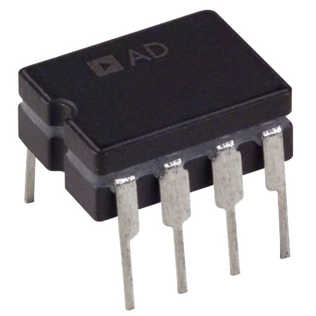
Plastic DIP and SOIC Packages
Cerdip Package
Die Form
MIL-STD-883B Processing
Tape & Reel (EIA-481A Standard)
Dual Version Available: AD827 (8 Lead)
Enhanced Replacement for LM6361
Replacement for HA2544, HA2520/2/5 and EL2020
APPLICATIONS
Video Instrumentation
Imaging Equipment
Copiers, Fax, Scanners, Cameras
High Speed Cable Driver
High Speed DAC and Flash ADC Buffers
CONNECTION DIAGRAM
Plastic DIP (N),
Small Outline (R) and
Cerdip (Q) Packages
specifications which include an open-loop gain of 3500 V/V
(500 Ω load) and low input offset voltage of 0.5 mV. Commonmode rejection is a minimum of 78 dB. Output voltage swing is
± 3 V into loads as low as 150 Ω. Analog Devices also offers
over 30 other high speed amplifiers from the low noise AD829
(1.7 nV/√Hz) to the ultimate video amplifier, the AD811, which
features 0.01% differential gain and 0.01° differential phase.
APPLICATION HIGHLIGHTS
1. As a buffer the AD847 offers a full-power bandwidth of
12.7 MHz (5 V p-p with ± 5 V supplies) making it outstanding as an input buffer for flash A/D converters.
PRODUCT DESCRIPTION
The AD847 represents a breakthrough in high speed amplifiers
offering superior ac & dc performance and low power, all at low
cost. The excellent dc performance is demonstrated by its ± 5 V
2. The low power and small outline package of the AD847
make it very well suited for high density applications such as
multiple pole active filters.
3. The AD847 is internally compensated for unity gain operation and remains stable when driving any capacitive load.
QUIESCENT CURRENT – mA
6
5.5
5
4.5
4
0
5
10
15
SUPPLY VOLTAGE – ± Volts
20
Quiescent Current vs. Supply Voltage
AD847 Driving Capacitive Loads
Information furnished by Analog Devices is believed to be accurate and
reliable. However, no responsibility is assumed by Analog Devices for its
use, nor for any infringements of patents or other rights of third parties
which may result from its use. No license is granted by implication or
otherwise under any patent or patent rights of Analog Devices.
One Technology Way, P.O. Box 9106, Norwood, MA 02062-9106, U.S.A.
Tel: 617/329-4700
Fax: 617/326-8703
REV. F
�AD847–SPECIFICATIONS (@ T = +258C, unless otherwise noted)
A
Model
Conditions
INPUT OFFSET VOLTAGE1
VS
±5 V
Min
AD847J
Typ
0.5
TMIN to TMAX
Offset Drift
Min
15
INPUT BIAS CURRENT
INPUT OFFSET CURRENT
6.6
7.2
3.3
6.6
10
µA
µA
± 5 V, ± 15 V
50
300
400
50
300
500
nA
nA
nA/°C
Offset Current Drift
0.3
VOUT = ± 2.5 V
RLOAD = 500 Ω
TMIN to TMAX
RLOAD = 150 Ω
VOUT = ± 10 V
RLOAD = 1 kΩ
TMIN to TMAX
DYNAMIC PERFORMANCE
Unity Gain Bandwidth
2
Slew Rate3
Settling Time
to 0.1%, RLOAD = 250 Ω
VOUT = 5 V p-p
RLOAD = 500 Ω,
VOUT = 20 V p-p,
RLOAD = 1 kΩ
RLOAD = 1 kΩ
Units
mV
mV
µV/°C
3.3
TMIN to TMAX
OPEN-LOOP GAIN
AD847AR
Typ
Max
0.5
1
4
15
± 5 V, ± 15 V
TMIN to TMAX
Full Power Bandwidth
Max
1
3.5
0.3
±5 V
2
1
3.5
2
1
1.6
± 15 V
3
1.5
3.5
V/mV
V/mV
V/mV
1.6
5.5
3
1.5
5.5
V/mV
V/mV
±5 V
± 15 V
35
50
35
50
MHz
MHz
±5 V
12.7
12.7
MHz
± 15 V
±5 V
± 15 V
4.7
200
300
4.7
200
300
MHz
V/µs
V/µs
225
225
–2.5 V to +2.5 V
10 V Step, AV = –1
–2.5 V to +2.5 V
10 V Step, AV = –1
CLOAD = 10 pF
RLOAD= 1 kΩ
f ≈ 4.4 MHz, RLOAD = 1 kΩ
f ≈ 4.4 MHz, RLOAD = 1 kΩ
±5 V
± 15 V
±5 V
± 15 V
± 15 V
65
65
140
120
65
65
140
120
ns
ns
ns
ns
± 15 V
± 15 V
50
0.04
0.19
50
0.04
0.19
Degree
%
Degree
COMMON-MODE REJECTION
VCM = ± 2.5 V
VCM = ± 12 V
TMIN to TMAX
±5 V
± 15 V
POWER SUPPLY REJECTION
VS = ± 5 V to ± 15 V
TMIN to TMAX
INPUT VOLTAGE NOISE
f = 10 kHz
± 15 V
INPUT CURRENT NOISE
f = 10 kHz
to 0.01%, RLOAD = 250 Ω
Phase Margin
Differential Gain
Differential Phase
INPUT COMMON-MODE
VOLTAGE RANGE
78
78
75
95
95
78
78
75
95
95
dB
dB
dB
75
72
86
75
72
86
dB
dB
15
15
nV/√Hz
± 15 V
1.5
1.5
pA/√Hz
±5 V
+4.3
–3.4
+14.3
–13.4
+4.3
–3.4
+14.3
–13.4
V
V
V
V
3.6
3
± 15 V
32
32
±V
±V
±V
±V
mA
INPUT RESISTANCE
300
300
kΩ
INPUT CAPACITANCE
1.5
1.5
pF
15
15
Ω
OUTPUT VOLTAGE SWING
RLOAD = 500 Ω
RLOAD = 150 Ω
RLOAD = 1 kΩ
RLOAD = 500 Ω
Short-Circuit Current
OUTPUT RESISTANCE
±5 V
±5 V
± 15 V
± 15 V
± 15 V
3.0
2.5
12
10
Open Loop
POWER SUPPLY
Operating Range
Quiescent Current
±5 V
TMIN to TMAX
3.6
3
64.5
± 15 V
TMIN to TMAX
4.8
5.3
3.0
2.5
12
10
618
6.0
7.3
6.3
7.6
64.5
4.8
5.3
618
6.0
7.3
6.3
7.6
V
mA
mA
mA
mA
NOTES
l
Input Offset Voltage Specifications are guaranteed after 5 minutes at T A = +25°C.
Full Power Bandwidth = Slew Rate/2 π VPEAK.
3
Slew Rate is measured on rising edge.
All min and max specifications are guaranteed. Specifications in boldface are 100% tested at final electrical test.
Specifications subject to change without notice.
2
–2–
REV. F
�AD847
Model
Conditions
INPUT OFFSET VOLTAGE1
VS
±5 V
Min
TMIN to TMAX
Offset Drift
INPUT BIAS CURRENT
AD847AQ
Typ
Max
0.5
1
4
15
Full Power Bandwidth2
Slew Rate3
Settling Time
to 0.1%, RLOAD = 250 Ω
to 0.01%, RLOAD = 250 Ω
Phase Margin
Differential Gain
Differential Phase
15
3.3
5
7.5
µA
µA
± 5 V, ± 15 V
50
300
400
50
300
400
nA
nA
nA/°C
0.3
DYNAMIC PERFORMANCE
Unity Gain Bandwidth
VOUT = 5 V p-p
RLOAD = 500 Ω,
VOUT = 20 V p-p,
RLOAD = 1 kΩ
RLOAD = 1 kΩ
–2.5 V to +2.5 V
10 V Step, AV = –1
–2.5 V to +2.5 V
10 V Step, AV = –1
CLOAD = 10 pF
RLOAD= 1 kΩ
f ≈ 4.4 MHz, RLOAD = 1 kΩ
f ≈ 4.4 MHz, RLOAD = 1 kΩ
COMMON-MODE REJECTION
VCM = ± 2.5 V
VCM = ± 12 V
TMIN to TMAX
POWER SUPPLY REJECTION
VS = ± 5 V to ± 15 V
TMIN to TMAX
Units
mV
mV
µV/°C
5
7.5
Offset Current Drift
VOUT = ± 2.5 V
RLOAD = 500 Ω
TMIN to TMAX
RLOAD = 150 Ω
VOUT = = ± 10 V
RLOAD = 1 kΩ
TMIN to TMAX
Max
1
4
3.3
TMIN to TMAX
OPEN-LOOP GAIN
AD847S
Typ
0.5
± 5 V, ± 15 V
TMIN to TMAX
INPUT OFFSET CURRENT
Min
0.3
±5 V
2
1
3.5
2
1
1.6
± 15 V
3
1.5
3.5
V/mV
V/mV
V/mV
1.6
5.5
3
1.5
5.5
V/mV
V/mV
±5 V
± 15 V
35
50
35
50
MHz
MHz
±5 V
12.7
12.7
MHz
± 15 V
±5 V
± 15 V
4.7
200
300
4.7
200
300
MHz
V/µs
V/µs
225
225
±5 V
± 15 V
±5 V
± 15 V
± 15 V
65
65
140
120
65
65
140
120
ns
ns
ns
ns
± 15 V
± 15 V
50
0.04
0.19
50
0.04
0.19
Degree
%
Degree
±5 V
± 15 V
80
80
75
95
95
80
80
75
95
95
dB
dB
dB
75
72
86
75
72
86
dB
dB
INPUT VOLTAGE NOISE
f = 10 kHz
± 15 V
15
15
nV/√Hz
INPUT CURRENT NOISE
f = 10 kHz
± 15 V
1.5
1.5
pA/√Hz
±5 V
+4.3
–3.4
+14.3
–13.4
+4.3
–3.4
+14.3
–13.4
V
V
V
V
3.6
3
INPUT COMMON-MODE
VOLTAGE RANGE
± 15 V
OUTPUT VOLTAGE SWING
RLOAD = 500 Ω
RLOAD = 150 Ω
RLOAD = 1 kΩ
RLOAD = 500 Ω
Short-Circuit Current
±5 V
±5 V
± 15 V
± 15 V
± 15 V
3.0
2.5
12
10
INPUT RESISTANCE
INPUT CAPACITANCE
OUTPUT RESISTANCE
Open Loop
POWER SUPPLY
Operating Range
Quiescent Current
±5 V
TMIN to TMAX
± 15 V
TMIN to TMAX
REV. F
–3–
32
32
±V
±V
±V
±V
mA
300
300
kΩ
3.6
3
3.0
2.5
12
10
1.5
1.5
pF
15
15
Ω
64.5
4.8
5.3
618
5.7
7.0
6.3
7.6
64.5
4.8
5.3
618
5.7
7.8
6.3
8.4
V
mA
mA
mA
mA
�AD847
ABSOLUTE MAXIMUM RATINGS 1
ESD SUSCEPTIBILITY
Supply Voltage . . . . . . . . . . . . . . . . . . . . . . . . . . . . . . . . ± 18 V
Internal Power Dissipation2
Plastic (N) . . . . . . . . . . . . . . . . . . . . . . . . . . . . . . 1.2 Watts
Small Outline (R) . . . . . . . . . . . . . . . . . . . . . . . . . 0.8 Watts
Cerdip (Q) . . . . . . . . . . . . . . . . . . . . . . . . . . . . . . 1.1 Watts
Input Voltage . . . . . . . . . . . . . . . . . . . . . . . . . . . . . . . . . . . ± VS
Differential Input Voltage . . . . . . . . . . . . . . . . . . . . . . . . ± 6 V
Storage Temperature Range (Q) . . . . . . . . . –65°C to +150°C
(N, R) . . . . . . . . . . . . . . . . . . . . . . . . . . . –65°C to +125°C
Junction Temperature . . . . . . . . . . . . . . . . . . . . . . . . . . 175°C
Lead Temperature Range (Soldering 60 sec) . . . . . . . +300°C
ESD (electrostatic discharge) sensitive device. Electrostatic
charges as high as 4000 volts, which readily accumulate on the
human body and on test equipment, can discharge without detection. Although the AD847 features proprietary ESD protection circuitry, permanent damage may still occur on these
devices if they are subjected to high energy electrostatic discharges. Therefore, proper ESD precautions are recommended
to avoid any performance degradation or loss of functionality.
NOTES
1
Stresses above those listed under “Absolute Maximum Ratings” may cause
permanent damage to the device. This is a stress rating only, and functional
operation of the device at these or any other conditions above those indicated in
the operational section of this specification is not implied. Exposure to absolute
maximum rating conditions for extended periods may affect device reliability.
2
Mini-DIP Package: θJA = 100°C/Watt; θJC = 33°C/Watt
Cerdip Package: θJA = 110°C/Watt; θJC = 30°C/Watt
Small Outline Package: θJA = 155°C/Watt; θJC = 33°C/Watt
METALIZATION PHOTOGRAPH
Contact factory for latest dimensions.
Dimensions shown in inches and (mm).
ORDERING GUIDE
Models*
Temperature
Range – 8C
Package
Description
Package
Option
AD847JN
AD847JR
AD847AQ
AD847AR
AD847SQ
AD847SQ/883B
5962-8964701PA
0 to +70
0 to +70
–40 to +85
–40 to +85
–55 to +125
–55 to +125
–55 to +125
Plastic
SOIC
Cerdip
SOIC
Cerdip
Cerdip
Cerdip
N-8
R-8
Q-8
R-8
Q-8
Q-8
Q-8
*AD847 also available in J and S grade chips, and AD847JR and AD847AR are available
*in tape and reel.
–4–
REV. F
�AD847
Typical Characteristics (@ +258C and V = 615 V, unless otherwise noted)
S
20
OUTPUT VOLTAGE SWING – Volts
INPUT COMMON-MODE RANGE – ± Volts
20
15
+VIN
10
–VIN
5
15
+VOUT
10
–VOUT
5
R LOAD = 500Ω
0
0
0
5
15
10
0
20
5
SUPPLY VOLTAGE – ± Volts
Figure 1. Input Common-Mode Range vs. Supply Voltage
20
Figure 2. Output Voltage Swing vs. Supply Voltage
30
OUTPUT VOLTAGE SWING – Volts p-p
15
10
SUPPLY VOLTAGE – ± Volts
6
QUIESCENT CURRENT – mA
25
20
±15 V SUPPLIES
15
10
±5V SUPPLIES
5
0
5.5
5
4.5
4
10
100
1k
10k
0
LOAD RESISTANCE – Ω
100
OUTPUT IMPEDANCE – Ω
INPUT BIAS CURRENT – µA
20
Figure 4. Quiescent Current vs. Supply Voltage
5
4
VS = ± 5V
3
10
1
0.1
0.01
–40
–20
0
20
40
60
80
100
120
140
10k
TEMPERATURE – °C
100k
1M
10M
100M
FREQUENCY – Hz
Figure 6. Output Impedance vs. Frequency
Figure 5. Input Bias Current vs. Temperature
REV. F
15
10
SUPPLY VOLTAGE – ± Volts
Figure 3. Output Voltage Swing vs. Load Resistance
2
–60
5
–5–
�AD847–Typical Characteristics (@ +258C and V = 615 V, unless otherwise noted)
S
35
SHORT CIRCUIT CURRENT LIMIT – mA
6
5
4
VS = ± 5V
3
–60
–40
–20
0
20
40
60
80
100
120
30
25
20
15
–60
140
–40
–20
TEMPERATURE – °C
100
140
+100°
80
+80°
±15V SUPPLIES
1kΩ LOAD
51
OPEN -LOOP GAIN – dB
UNITY – GAIN BANDWIDTH – MHz
52
50
49
60
+60°
±5V SUPPLIES
500Ω LOAD
40
+40°
20
+20°
0
48
–60
120
Figure 8. Short-Circuit Current Limit vs. Temperature
Figure 7. Quiescent Current vs. Temperature
0
–20
–40
–20
0
20
40
60
80
100
120
100
140
1k
10k
100k
1M
FREQUENCY – Hz
TEMPERATURE – °C
Figure 9. Gain Bandwidth Product vs. Temperature
10M
100M
Figure 10. Open-Loop Gain and Phase Margin
vs. Frequency
80
100
POWER SUPPLY REJECTION – dB
VS = ±15V
75
OPEN-LOOP GAIN – dB
0
20
40
60
80
100
AMBIENT TEMPERATURE – °C
PHASE MARGIN – DEGREES
QUIESCENT CURRENT – mA
7
70
VS = ± 5V
65
60
55
50
10
100
1k
+SUPPLY
80
60
–SUPPLY
40
20
0
10k
1k
LOAD RESISTANCE – Ω
Figure 11. Open-Loop Gain vs. Load Resistance
10k
100k
1M
FREQUENCY – Hz
10M
100M
Figure 12. Power Supply Rejection vs. Frequency
–6–
REV. F
�AD847
100
80
OUTPUT VOLTAGE – Volts p–p
30
VCM = ±1V p-p
CMR – dB
60
40
20
25
20
RL = 1kΩ
15
10
5
0
0
1k
10k
100k
1M
10M
1M
100M
10M
100M
INPUT FREQUENCY – Hz
FREQUENCY – Hz
Figure 14. Large Signal Frequency Response
Figure 13. Common-Mode Rejection vs. Frequency
–70
10
HARMONIC DISTORTION – dB
OUTPUT SWING FROM 0 TO ± V
8
6
4
2
1%
0.1%
1%
0.1%
0
–2
–4
–6
–80
3V RMS
R L=1kΩ
–90
2ND HARMONIC
–100
–110
3RD HARMONIC
–120
–8
–130
100
–10
0
20
40
60
80
100
120
140
160
1k
SETTLING TIME – ns
Figure 15. Output Swing and Error vs. Settling Time
450
400
40
SLEW RATE – V/µs
Hz
INPUT VOLTAGE NOISE – nV/
100k
Figure 16. Harmonic Distortion vs. Frequency
50
30
20
10
350
300
250
200
150
–60
0
10
100
1k
10k
100k
1M
10M
–40
–20
0
20
40
60
80
100
120
TEMPERATURE – °C
FREQUENCY – Hz
Figure 18. Slew Rate vs. Temperature
Figure 17. Input Voltage Noise Spectral Density
REV. F
10k
FREQUENCY – Hz
–7–
140
�AD847
Figure 19. Inverting Amplifier Configuration
Figure 19a. Inverter Large
Signal Pulse Response
Figure 19b. Inverter Small
Signal Pulse Response
Figure 20. Noninverting Amplifier Configuration
Figure 20a. Noninverting
Large Signal Pulse Response
Figure 20b. Noninverting
Small Signal Pulse Response
–8–
REV. F
�AD847
OFFSET NULLING
+VS
The input offset voltage of the AD847 is very low for a high
speed op amp, but if additional nulling is required, the circuit
shown in Figure 21 can be used.
CF
OUTPUT
–IN
+IN
–VS
Figure 21. Offset Nulling
NULL 1
NULL 8
INPUT CONSIDERATIONS
An input resistor (RIN in Figure 20) is required in circuits where
the input to the AD847 will be subjected to transient or continuous overload voltages exceeding the ± 6 V maximum differential limit. This resistor provides protection for the input
transistors by limiting the maximum current that can be forced
into their bases.
Figure 22. AD847 Simplified Schematic
GROUNDING AND BYPASSING
In designing practical circuits with the AD847, the user must
remember that whenever high frequencies are involved, some
special precautions are in order. Circuits must be built with
short interconnect leads. A large ground plane should be used
whenever possible to provide a low resistance, low inductance
circuit path, as well as minimizing the effects of high frequency
coupling. Sockets should be avoided because the increased
interlead capacitance can degrade bandwidth.
For high performance circuits it is recommended that a resistor
(RB in Figures 19 and 20) be used to reduce bias current errors
by matching the impedance at each input. The offset voltage error will be reduced by more than an order of magnitude.
THEORY OF OPERATION
Feedback resistors should be of low enough value to assure that
the time constant formed with the capacitance at the amplifier
summing junction will not limit the amplifier performance.
Resistor values of less than 5 kΩ are recommended. If a larger
resistor must be used, a small (